JETIRJ006032 Journal of Emerging Technologies and Innovative Research (JETIR) www.jetir.org 197
Abstract. Involvement for an intellectual property (IP) core assessment demonstrates diverse methodologies that can be implement for utilization of IP- core in CEH (Complex Electronic Hardware) and these should reflect to design level at which IP is conveyed (soft, firm, hard) and basically reminds on the availability to the design data. Using an IP-core or utilizing inside the airborne electronic hardware, the IP user ought to pick the most suitable approaches to assuring that the IP will satisfy the design affirmation goals. This paper gives data on the methodologies that can be utilized, or the testing of IP core as per DO-254 measurements and these measurements how to verify in to possible condition like reset scenario to verify critical module or functionalities under hardware requirements. The main objective of this paper is the Target level testing of IP CORE, it will be analyzed by capturing and verifying the data, whether transmitted data contains proper values by the use of analyzer tool. The efficacy of the data is demonstrated with graphic controller as a case study.
Keywords: FPGA, IP core, Chip Scope Pro analyzer Tool, Test Cases, FIFO, VHDL.
1
IntroductionRecently testing the soft IP core is the category of IP-core that comes to the user with the most life-cycle data. This data generally include register transfer level (RTL) descriptions in languages such as Verilog or VHDL. This allows a detailed analysis and optimization (and eventually customization) of the soft IP-cores for the intended application. Soft IP-cores still need to be synthesized placed and routed (P & R) in the target Airborne Electronics Hardware (AEH) device. The differentiation among Soft, Firm and Hard IPs are depicted in Figure.1.
This paper discuss about the verification under soft IP core by demonstrating graphical controller by capturing all possible test case as part of this paper, seeing the possible test cases of particular functionality as per hardware requirements and dumping in to target level of testing which is for accuracy, helps in better time to market [4]
Soft IP Firm IP Hard IP
Fig.1. As per hardware activities among the Soft IP-core takes place [5]
1.1. Verification of critical functionalities
This Controller module captures the graphical information (red_i, green_i and blue_i) as inputs and computes graphical timing parameters required for the video frame generation based on the control signals such as HSync_i, VSync_i and DataEn_i. The graphical timing parameters such as lines_count_o, pixels_count_o, horsync_width_o, horBP_width_o, horFP_width_o, horactive_width_o, vertsync_width_o, vertBP_width_o, vertFP_width_o, vertactive_width_o and Video_fps_o are sent to the storing parameters and the registered pixel information such as Red_o,Green_o , Blue_o, HSync_o , VSync_o and DataEn_o are sent to the further module for further process [2]
Requirements RTL
Design
Pre-Layout Synthesis Netlist
Place & Route
Final Binary File
Post- Layout Netlist Design
JETIRJ006032 Journal of Emerging Technologies and Innovative Research (JETIR) www.jetir.org 198
Fig.2. Block diagram of graphic controller as critical module [3]
This block shall be used for storing R (8bit) component, G(8bit) component, & B(8bit) component obtained from graphics driver (SXGA+) to produce the color spectrum as well as an input of pixel clock, V_SYNC, H_SYNC, data_en, R (8bit) component, G(8bit) component, & B(8bit) component. Pixel clock shall be obtained as follows:
Pixel clock = (total no:of pixel in a line * total no:of lines in whole frame * refresh rate) as shown in below Table.1. H_SYNC signal shall indicate the start of row timing within a video frame, & it shall scan row by row until it reduces the end of the frame and V_SYNC signal shall indicate the start of a video frame, one V_sync scan from top to bottom shall generate one image. The controller block shall have a global reset to reset the IP-Core. Data_en shall be in SYNC with pixel generation module block. It shall concatenate R (8bit) component, G(8bit) component, & B(8bit) component 24 bit RGB data and generate V_sync, which shall be given to V_sync delayer, reset, &SOF Gen block for timing requirement of frame.There shall be FIFO reset from the V_sync delayer reset and SOF Gen block to reset the FIFO block as shown in Figure 2.
The RGB color estimation of a pixel is generally spoken to on a PC as three bytes: one for red, one for green, and one for blue. These qualities, in any case, are advanced: in request to change over a computerized an incentive to a simple voltage, our VGA controller will utilize a co digital-to-analog converter, or DAC. The VGA module on the SPARTAN6s (alluded to as the XSGA module) has three extraordinary rapid DACs fit for changing over eight- bit digital color esteems to a simple voltage from 0V to 0.7V. So as to send video information over VGA to an outer screen, we will plan a controller to interface with this XSGA module. With a specific end goal to separate between successive pixels, a Graphics controller will utilize two signals to keep up synchronization with the monitor. These two signals are normally alluded to as HSYNC (horizontal sync) and VSYNC (vertical sync). The screen begins attracting the picture the upper left corner, which in PC illustrations, is normally thought to be the origin (0, 0) of the coordinate space. A pulse of the HSYNC signal teaches the screen to move down to the following column/line. Between HSYNC pulses, the screen utilizes the simple voltages for R, G, and B to decide the color of every pixel in a level column. Once every column on the screen is drawn, the controller will send a VSYNC pulse, which trains the screen to restart at the beginning (upper left corner). The quantity of VSYNC beats in a moment is the same as the “refresh rate" of the video motion, as each compares to the show being redrawn.
2.
Test casesThe test cases are generated for the Normal, Boundary and Robustness cases for functional verification to cover the Hardware Design Data requirements which are mentioned in the Table.2.
The test inputs for the normal, boundary, robustness are provided in the following sections. The test cases are generated for the normal functional verification that covers the Hardware design Data requirements which are mentioned in the Table.2. The test cases are written for all the possible combinations of reset signal (Areset_i) and control signals (HSync_i, VSync_i and Data_en_i). The RGB input pixel data that are passes from input port as 8bit which is passed output as it 8 bit data format at the output port and also (HSync_i, VSync_i and Data_en_i) is passed as it is at the output port. The following section will describe the steps to generate the VESA standard signals, test cases and test procedures.
Steps to follow to generate the HSync, VSync, DataEn signals and RGB data as per VESA standards.
1. Add the Xilinx libraries.2. Use IEEE.STD_LOGIC_arith.ALL.3.Use std.textio.all; 4. The following two libraries are to capturing the local signals library modelsim_lib. Use modelsim_lib.util.all;
Clock period definition in the Architecture Behavioral structure to be changed as given below
clk_i period: Time: = 8.15 ns --pixel clk input (clk_i= 122.61 MHZ)
JETIRJ006032 Journal of Emerging Technologies and Innovative Research (JETIR) www.jetir.org 199
Step 1: Condition to generate the H_sync_i H_sync_i = 1 (for H_count >= 0 and < 152) Step 2: Condition to generate the V_sync_i V_sync_i = 1 (for V_count >= 0 and < 3) V_sync_i = 0 (for V_count >= 3 and < 1086) Step 3: Condition to generate the data_en_i
Data_en_i = 1 (for H_count >= 391 and < 1792) & (for V_count >= 35 and < 1086) Data_en_i = 0 other condition Case 3
When A_reset_i = 0 the following graphical parameters will be computed and updated with every positive edge of V_sync, lines_count_o, pixel_count_o, Hor_sync_width_o, , horBP_width_o, horFP_width_o, horactive_width_o, vertsync_width_o, vertBP_width_o, vertFP_width_o, vertactive_width_o and Video_fps_o.
(Here the reset (Areset_i) will be 0 and the input will be given for standard VESA timings and output will be the, computed graphical parameters (without video_fps_o) which is interfaced with configuration status handler and RGB (each 8 bit), data_enable, Hsync, Vsync are passed as it is at output port with one clock delay, which is interface to pixel generation.
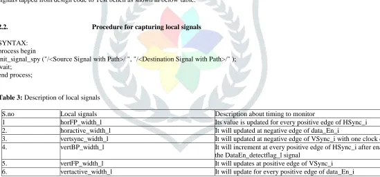
Note: Limitations: DUT local signals can’t be observed in the Test Bench and with assertion (only input and output signals of DUT can be observed in Test Bench). Local signal can be observed in the simulated waveform and it can’t be logged. Local signals tapped from design code to Test bench as shown in below table.
2.2. Procedure for capturing local signals
SYNTAX: process begin
init_signal_spy ("/<Source Signal with Path>/ ", "/<Destination Signal with Path>/" ); wait;
end process;
Table 3: Description of local signals
S.no Local signals Description about timing to monitor
1 horFP_width_l Its value is updated for every positive edge of HSync_i
2. horactive_width_l It will updated at negative edge of data_En_i
3. vertsync_width_l It will updated at negative edge of VSync_i with one clock delay 4. vertBP_width_l It will increment at every positive edge of HSync_i after enabling
the DataEn_detectflag_l signal
5. vertFP_width_l It will updates at positive edge of VSync_i
6. vertactive_width_l It will update for every positive edge of data_En_i
3.
Testing process of critical functionalities for an IP-coreThese process will be analyzed by capturing the packets and verifying the data, whether transmitted packets contains a proper values by the use of chip scope pro analyzer tool.
JETIRJ006032 Journal of Emerging Technologies and Innovative Research (JETIR) www.jetir.org 200 Generate ICON,
ILA, VI O or ATC2 Cores
Instantiates cores into HDL
source
Synthesis Design without instantiating
chip scope cores
Synthesis design with
cores in it
Connect bus & internal signals to cores INSERT …I CON, ILA or ATC2 into
synthesized design (.ngc or EDIF net
list)
ISE Implement
Select – Bit Stream set – trigger View – wave for m
3.1. Test environment
Take the Soft IP Core from the SCM path. Instrument the Soft IP Core for testing the end-end functionality then Re-generate the IP Core checksum after Download the Instrumented IP Core on to the SPARTAN 6 target using the procedure xxxx. Provide this procedure which is Inject the test pattern as per the procedure, Observe/ Collect the output data as per the procedure and Generate the test report.
Integrate logic analyzer (ILA) , which is used to debug the interfaces between intermediate blocks among them. Core generator tool, the ILA core is customizable logic analyzer core that can be used to monitor any internal signal of your design.
There are important parameters in ILA core, Firstly Trigger input logic and output logic i.e. Trigger input logic can detect elobrate trigger events and Trigger output logic can be triggers external test equipment and other logic. Secondly Data capture logic i.e. ILA core capture and store trace data information using on-chip BRAM resources and Control and status logic which manages the operation of the ILA core.
Fig.3: Chip Scope Flow for analyzing the waveform
3.2. Testing approach at target level of IP-core
Testing with instrumented code is integrated with Tx IP-core code and Rx IP-core code. Instrumented code is used to inject failures on the fly to simul.ate the failure scenarios. F Figure shows the top block is a wrapper block, receives the input DVI sources. Wrapper then converts it to the RGB & control signals as output. These output signals are interfaced to the instrumented top block [6] as shown in below Figure.4.
Fig.4. Operation of instrumented code .
The instrumented code will change the original input signal timing pattern and feed to the original source code to test the IP-core behavioral and observe the output. Different IP core will be tested for the possible signals and output will be observed. Flow of signal and data is shown in Figure 5. [7]
JETIRJ006032 Journal of Emerging Technologies and Innovative Research (JETIR) www.jetir.org 201
varying the DataEn_i signal as shown in Table.5.
Fig.6. Generation of parameters of graphical controller
5.
ConclusionFor the advancement of incorporated test frameworks there are currently accessible intense devices that permit having both, the essential equipment for interfacing and, the advancement condition for the execution of test arrangements. By picking a secluded test framework that permits for simple mix of various sorts of equipment, counting that created by outsiders, you can have an effortlessly upgradeable and configurable single seat that incorporates useful and limit examine testing, enhancing the unwavering quality of the tests, as well as their cost and span.
Fig.7. Operation of Logic Scope in to IP core
References
1. Thompson S., “VGA—Sign Choices for a New Video Subsystem”, IBM Systems Journal Vol.27,
Issue. 2, Page(s) 185-190, 1988.
2. Van-Huan Tran, Xuan-Tu Tran, “An Efficient Architecture Design for VGA Monitor Controller”, IEEE International Conference on Consumer Electronics, Communications and Networks (CECNet), Page(s) 3921-3927, 2011
3. Radi H.R., Caleb W.W.K., M.N.Shah Zainudin., M.Muzafar Ismail, “The Design and Implementation of VGA Controller on FPGA”, International Journal of Electrical & Computer Sciences IJECS- IJENS, Vol. 12, Page(s) 56-60, 2012.
5. CAST. “High Resolution Display Controller – Datasheet”.Technical report, October 2010.
4. “Think Silicon Ltd. Think LCD Display Controller – Product Specification.” Technical report,
2010.
JETIRJ006032 Journal of Emerging Technologies and Innovative Research (JETIR) www.jetir.org 202
Specification, July 2008.
6. Richard Herveille. “VGA/LCD Controller v2.0.” Technical Report, 2009.
7. Guohui Wang, Yong Guan, and Yan Zhang. “Designing of VGA Character String Display Module Based on FPGA.”, IEEE International Symposium on Intelligent Ubiquitous Computing and Education(IUCE), Page(s) 499–502, 2009.
8. Javier Valcarce Garcia. “Monochrome Text-Mode VGA Video Display Adapter.” Technical Report, 2009.
9. Chacko B.T, Shelly S., “Real-Time Video Filtering and Overlay Character Generation on FPGA