ISSN : 2230-7109 (Online) | ISSN : 2230-9543 (Print)
Design and Simulation of Novel Full Adder
Cells using Modified GDI Cell
1
John George Victor,
2Dr. M Sunil Prakash
1,2Dept. of ECE, MVGR College of Engineering, Vizianagaram, India
Abstract
This paper presents low-power, low voltage and high speed 1-bit full adder circuits is proposed. Our approach is based on XOR-XNOR design full adder circuits in a single unit as well as Gate Diffusion Input techniques. Using 3transistor XOR Gate Logic style 8T,9T and 12T full adder cell are designed, which increases the speed and performance and reduces power dissipation at lower supply voltage. The design of 5 different full adder topologies using Modified Gate Diffusion Input (MGDI) Technique is reviewed in this paper. This MGDI technique allows the circuit to consume less power, less delay and to get optimized area of digital circuits, while maintaining low complexity of logic design. The simulations are carried out using 130nm CMOS Technology of Mentor Graphics. Analysis and evaluation is carried out for various adder circuit and their performances are compared by varying supply voltages. Simulation results illustrates that proposed adders have better performance, Low power, High speed against other designed adder circuits like CCMOS, CPL, TGA and Hybrid adder circuits.
Keywords
Full adder, XOR-XNOR circuit, High Speed, Low Power, Very Large Scale Integrated Circuits
I. Introduction
For any arithmetic operation an addition is a very basic operation. Many well-known operations such as Subtraction, multiplication, division and address calculation are based on addition. The full adder cell is a basic building block of the binary adder which is widely used in many VLSI applications. The main and significant goal of VLSI designer to enhance the performance of the 1-bit full-adder to its best. From the literature a vast variety of full-full-adders using different logic styles and technologies have been reported [1-8] and they commonly aim at reducing power consumption and increasing speed. Among these adders the circuits explained below will be used for comparison in this paper. Though these full adder cells perform the similar function but design, transistor count, production of intermediate node and output are important factors for a designer. Different logic styles tend to favor one performance aspect at the expense of the other. A full adder cell can be designed by using one logic style alone or sometimes it uses more than one logic style for their implementation. In altogether main purpose of the full-adders cell designer to reduce number of transistor, power consumption and delay factors which in turn reduces power-delay product (PDP) in comparison to the previous ones.
The most conventional one is complementary CMOS full-adder (C-CMOS). It is based on regular CMOS structure with pull-up and pull-down transistors and has 28 transistors. Another conventional adder is the Complementary Pass-Transistor Logic (CPL) [7-9] with swing restoration which uses 32 transistors. The difference between the complementary CMOS logic styles and pass transistor logic is that the source side of the pass logic transistor network is connected to some input signals instead of the power lines. The Transmission Function Full-Adder (TFA) is proposed in [7,11] is based on transmission function theory
and transmission gates and has 16 transistors. Transmission gates [9,11] consist of a PMOS transistor and a NMOS transistor that are connected in parallel. Another Transmission Gate Full-Adder (TGA)[9,10] contains 20 transistors. TFA and TGA are inherently low power consuming and they are good for designing XOR or XNOR gates. The low driving capability of TGA and TFA circuit is the main disadvantage of using these logic styles. When TGA or TFA are cascaded, their performance degrades significantly. The 14-Transistor (14T) full-adder uses more than one logic style for their implementation called hybrid logic design style [10-11]. But output swing is the major point of concern in hybrid design as it suffers from the none full swing pass transistors with swing restored transmission gate techniques. The 10-Transistor (10T) full-adder [10] uses hybrid logic style similar to 14T. It has small transistor count but it is not full swing. In fan-out condition these hybrid full-adders and 14T full-adder suffer from the lack of driving capabilities which causes the performances degradation dramatically in cascaded stages. It must be stated that this full-adder cannot work properly when supply voltage is less than 1.8 V. Another full adder cell is hybrid full-adder [11]. In this design the pass logic circuit that generates the intermediate XOR and XNOR outputs has been improved which makes the full-adder cell to work at low supply voltage.
II. The GDI Cells Technique For full Adder
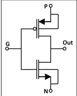
Gate-Diffusion-Input (GDI) method is based on the use of a simple cell as shown in fig. 1. A Gate diffusion Input Cell look similar to that of standard CMOS inverter at first glance but there are some importance and crucial differences:
GDI cell contains three inputs – G (common gate input of 1.
NMOS and PMOS), P (input to the source/drain of PMOS), and N (input to the source/drain of NMOS).Whereas in CMOS inverter it has only one input and one output.
P
G Out
t
N Fig. 1: Simple GDI Cell
Bulks of both NMOS and PMOS are connected to N or P 2.
Table 1: Some Logic Functions that can be Implemented With a Single GDI and MGDI CELL [12].
N P G Output Function
‘0’ B A
A
B
F1B ‘1’ A
A
+
B
F2‘1’ B A
A
+
B
ORB ‘0’ A AND
C B A MUX
‘0’ ‘1’ A
A
NOTTable 1 shows how a simple change of the input configuration of the simple GDI cell corresponds to very different Boolean functions. Most of these functions are complex (6-12 transistors) in CMOS, as well as in standard PTL implementations, but very simple (only 2 transistors per function) in GDI design method. III. Modified GDI(MGDI) Cell
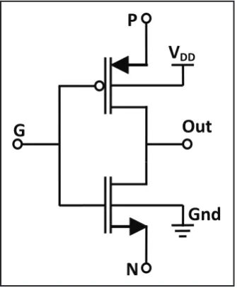
The basic primitive of MGDI cell is similar to that of GDI Cell which consists of nMOS and pMOS containing four terminals G (common gate input of nMOS and pMOS transistors), P (the outer diffusion node of pMOS transistor), N (the outer diffusion node of MOS transistor), and ‘Out’ (common diffusion node of both transistors). In modified primitive GDI cell body or substrate of the pMOS is connected to the Supply voltage VDD, and body of the nMOS is connected to the supply voltage ground. Whereas in GDI Cell, body of the pMOS is connected to the drain and body of nMOS is connected to source. This make the GDI to constant body biasing in modified GDI Cell which in turn increase the stability of the circuit and its loading effect. The logic gates have been implemented in 130nm CMOS technology and it is compared with existing GDI and CMOS logic.
P
G
Out
t
N
V
DDGnd
Fig. 2: Simple MGDI Cell
Fig. 2 shows the construction of modified GDI basic gates of AND, OR, NOR, NAND, XOR, XNOR and MUX as listed in Table I. As an example the operation of AND gate is elucidated. For AND gate the drain of pMOS is connected with input A and the source of nMOS is connected with input B. The Gate terminal G is connected
to the A. When both the inputs are zero the pMOS will operates in linear whereas nMOS in cur-off. While A = ‘1’ and B = ‘0’ the pMOS in cut-off and nMOS in linear. Similarly for A = ‘0’ and B = ‘1’ pMOS in linear and nMOS in cut-off. Therefore for A = ‘1’ and B = ‘1’ pMOS in linear and nMOS in linear thereby producing the output as 1.
The logical level for different input combination will be: For A = ‘0’ and B = ‘0’
pMOS in linear: Vin – Vtp<Vout< VDD. nMOS in cut-off: Vin<Vtn
For A = ‘1’ and B = ‘0’
pMOS in cut-off: Vin> VDD + Vtp. nMOS in linear: 0 <Vout< Vin - Vtn.
For A = ‘0’ and B = ‘1’
pMOS in linear: Vin – Vtp<Vout< VDD. nMOS in cut-off: Vin<Vtn For A = ‘1’ and B = ‘1’
pMOS in linear: Vin – Vtp<Vout< VDD. nMOS in linear: 0 <Vout< Vin - Vtn.
The performance analysis of MGDI, GDI and CMOS logic are evaluated and its performance comparison are made with respect to switching delay, transistor count and average power consumed by MGDI, GDI and CMOS logic. From this analysis it is observed that the modified GDI performance is better when comparing to GDI and CMOS logic. In CMOS the number of transistor used to realize a function is twice that of MGDI. The transistors used to design XOR and XNOR has only three transistors in MGDI whereas it is 8 in CMOS logic. The power consumed by CMOS is slightly higher than MGDI.
IV. Design of Modified GDI Full Adders
A full adder is a combinational circuit that performs the arithmetic sum of three bits: A, B and Cin, from a previous addition produces the corresponding SUM and Cout.
The various equations for SUM and CARRY are given below
(1)
C
A
C
B
B
A
C
out=
⋅
+
⋅
+
⋅
(2))
(
)
(
A
B
C
A
B
C
SUM
=
⊕
+
⊕
(3))
(
A
B
C
B
A
C
out=
⋅
+
in⊕
(4)C
B
A
B
A
B
ISSN : 2230-7109 (Online) | ISSN : 2230-9543 (Print)
the eq. (1) & (5), has been realized using 3-input XOR for sum expression and for carry expression 2-to-1 MUX have been used as shown in fig. 7.
Fig. 3: 20T MGDI Full Adder
Fig. 4:12T MGDI Hybrid Full Adder Cell
The proposed 5 different MGDI full adders are simulated using Mentor Graphics 130nm CMOS Technology by varying the supply voltage from 0.8V to 1.4V in steps of 0.1V. and keeping the threshold voltage of the transistor approximated at 0.34V.
Fig. 5: 10T MGDI full Adder Cell
Fig. 6: 9T MGDI Full adder cell
Fig. 7: 8T MGDI Full adder cell
MHz frequency and at 270C and the supply voltages varying from
0.8 to 1.4V using Mentor Graphics 130nm CMOS Technology and keeping the threshold voltage of the transistor approximated at 0.34V. The three inputs to the full adder are A, B and CIN and all the test vectors are generated and have been fed into the adder cell. the delay is measured from 50% of the input voltage swing to 50% of the output voltage swing SUM and CARRY. All transitions from an input combination to another (total 8 patterns 000, 001, 010, 011, 100, 101, 110, 111) have been tested, and the delay at each transition has been measured. The average has been reported as the cell delay.
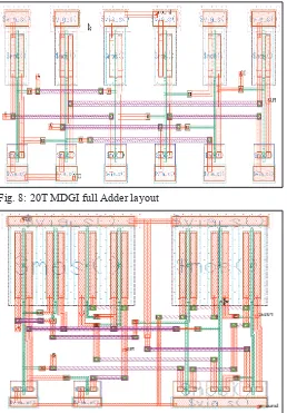
Fig. 8: 20T MDGI full Adder layout
Fig. 9: 12T MDGI full Adder Layout 4 Inverter (8T)are not shown)
Fig. 10: 10T MDGI full Adder Layout
Fig. 11: 9T MDGI full Adder Layout
Fig. 12: 8T MDGI full Adder Layout
ISSN : 2230-7109 (Online) | ISSN : 2230-9543 (Print)
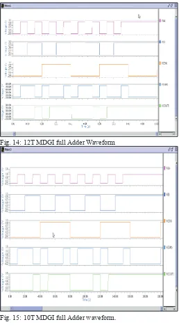
Fig. 14: 12T MDGI full Adder Waveform
Fig. 15: 10T MDGI full Adder waveform.
Fig. 16: 9T MDGI full Adder waveform.
Fig. 17: 8T MDGI full Adder waveform
The performances of different MGDI full adders have been analyzed in terms of delay, transistor count and power dissipation with respect to CMOS, pass transistor logic and GDI technique. It is observed that modified GDI full adder cells have least delay and power consumption when compared to CMOS, pass transistor logic and GDI technique. In the modified GDI adder cell it is observed that the design of XOR and XNOR has only 3 transistors when compare to GDI logic. An input transition may or may not result in change at the output node. Even if there is no switching at the output node, some internal node may be switching which results in power consumption. For an accurate result, all the required input pattern-to-input-pattern transitions are included in the test patterns. The power consumption value and delay are measured for the 1-bit bit adder cell. The input/output waveforms and layout of the all the 1 bit adder cell are shown in fig. 8 to 17.
Fig. 18: Power Results for Different Supply Voltages
Fig. 20: Power Delay Product Results for Different Supply Voltages
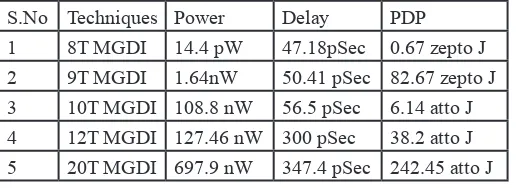
Table 2: Power, Delay and Power Delay Product for 5 different Modified GDI Full adder Cell and supply voltage VDD = 1.2V.
S.No Techniques Power Delay PDP 1 8T MGDI 14.4 pW 47.18pSec 0.67 zepto J 2 9T MGDI 1.64nW 50.41 pSec 82.67 zepto J 3 10T MGDI 108.8 nW 56.5 pSec 6.14 atto J 4 12T MGDI 127.46 nW 300 pSec 38.2 atto J 5 20T MGDI 697.9 nW 347.4 pSec 242.45 atto J Comparison of full adder cells is discussed below referred to Delay, Power and Power Delay Product(PDP). The values of delay obtained based on post layout simulation for considered values of (0.8–1.4 V) in 130nm CMOS Technology. Delay value of the 1-bit adder cells is illustrated. Tables II show the Power, Delay PDP values at 1.2 V for 130nm . It is apparent that among the existing full adders, the proposed 8T MGDI full adder cell has the smallest delay because of for 20T, 12T,10T, 9T and 8T MGDI full adder cells are determined under different supply voltages just having two transistors in the critical path for driving the output. The average power consumption (0.8–1.4 V) in 130 nm. The proposed 8T MGDI full adder cell shows the best performance among the above mentioned full adders under varying supply voltages. 8T MGDI full adder utilizes GDI structure as its main cell which has a lowest power consumer cells that is suitable for designing fast, Low Power circuits but also improves logic level swing and static power characteristics. Power-Delay-Product (PDP) is a quantitative measure of the efficiency and a compromise between power dissipation and speed. PDP is particularly important when low power operation is needed. The Power-Delay Product for 20T, 12T, 10T, 9T and 8T MGDI full adder cells are evaluated under different supply voltages (0.8–1.4 V) in 130nm. 8T MGDI full cell adder has the best PDP in comparison with its counterpart.
VI. Conclusion
An extensive performance analysis of Full adder cells using Modified GTE Diffusion Input (MGDI) is reviewed in this paper. The performance of these MGDI Full adder cells was analyzed in terms of transistor count, delay and power dissipation using Mentor Graphics 130nm CMOS technology and the results are compared with different MGDI Full adder cell such as 20T, 12T, 10T, 9T and 8T. The simulation results shows that 8Transistor
MGDI Full adder cells have less delay and low power consumption as compared to the other full adder cells. From this analysis it is observed that the full adder cells designed with MGDI has the transistor count of 16T, 14T, 12T, 10T and 8T. In MGDI the number of transistor required to implement XOR operation will be less in number only 3T whereas in GDI Cell 4 transistor are required. In case of CMOS the transistor count is approximately double that of MGDI adders. It can be observed that the power dissipation of the adder cell decreased, the transistor count decreased and delay of the cell is also reduced. Overall the simulation results shows that the full adder cell using modified GDI cell has least delay, low power consumption and less transistor count when compared with existing GDI, CMOS and PT logic.
References
[1] J. Wang, S. Fang, W. Feng,"New efficient designs for XOR and XNOR functions on the transistor level", IEEE J. of Solid-State Circuits 29 (7), pp. 780–786, 1994.
[2] R. Zimmermann, W. Fichtner,"Low-power logic styles: CMOS versus pass transistor logic", IEEE Journal of Solid-State Circuits 32 (7), pp. 1079–1089, 1997.
[3] J. Gu, C.H. Chang,"Low voltage, low-power (5:2) compressor cell for fast arithmetic circuits", Proceedings of the IEEE International Conference on Acoustics, Speech, and Signal Processing 2, pp. 661–664, 2003.
[4] K. Navi, M. Maeen, V. Foroutan, S. Timarchi, O. Kavehi, "A Novel low-power full-adder cell for low voltage", Integration, the VLSI Journal (2009)10.1016/ j.vlsi.2009.02.001. [5] A.M. Shams, M.A. Bayoumi,"A structured approach for
designing low-power adders", Proceedings of the 31st Asilomar Conference on Signals, Systems, and Computers 1, pp. 757–761, 1997.
[6] A. Shams, T. Darwish, M. Bayoumi,"Performance analysis of low power 1-bit CMOS full-adder cells", IEEE Transactions on Very Large Scale Integration (VLSI) Systems 10 (1) (2002 February) pp. 20–29.
[7] K. Navi, O. Kavehei, M. Rouholamini, A. Sahafi, S. Mehrabi, N. Dadkhahi,"Low power and high-performance 1 bit CMOS full-adder cell", Journal of Computers 3 (2), 2008 February.
[8] H. Veendrick,"Short circuit dissipation of static CMOS circuitry and its impact on the design of buffer circuits", IEEE Journal of Solid-State Circuits SC-19 (4), pp. 468–473, 1984.
[9] S. Heo, K. Asanovi ´c,"Leakage-biased domino circuits for dynamic finegrain leakage reduction", VLSI Circuits Symposium, Honolulu, HI, June 2002.
[10] R. Shalem, E. John, L. K. John,"A novel low-power energy recovery fulladder cell", In: Proceedings of the Great Lakes Symposium on VLSI, February 1999, pp. 380–383. [11] K. Navi, M.H. Moaiyeri, R. FaghihMirzaee, O. Hashemipour,
B. Mazloom Nezhad,"Two new low-power full-adders based on majority-not gates", Microelectronics Journal, Elsevier 40 (1), pp. 126–130, 2009.
ISSN : 2230-7109 (Online) | ISSN : 2230-9543 (Print)
John George Victor did his B.E. from Andhra University, Visakhapatnam in Electronics and Communication Engineering, Visakhapatnam. Presently pursuing Masters degree from Jawaharlal Nehru Technology University, Kakinada. His research interests include Low Power VLSI, VLSI system Design and Communications.