Int. J. Nanosci. Nanotechnol., Vol. 14, No. 4, Dec. 2018, pp. 277-288
Dynamic Simulation of CNTFET-Based Digital
Circuits
Roberto Marani1 and Anna Gina Perri2,*
1
Institute of Intelligent Industrial Technologies and Systems for Advanced Manufacturing (STIIMA), National Research Council of Italy.
2
Electronic Devices Laboratory, Department of Electrical and Information Engineering, Polytechnic University of Bari, Italy.
(*) Corresponding author: [email protected] (Received: 28 November 2017 and Accepted: 08 July 2018)
Abstract
In this paper we propose a simulation study to carry out dynamic analysis of CNTFET-based digital circuit, introducing in the semi-empirical compact model for CNTFETs, already proposed by us, both the quantum capacitance effects and the sub-threshold currents. To verify the validity of the obtained results, a comparison with Wong model was carried out. Our model may be easily implemented both in SPICE and in Verilog-A, obtaining, in this last case, the development time in writing the model shorter, the simulation run time much shorter and the software much more concise and clear than Wong model.
Keywords:CNTFET, Digital Design, Dynamic Analysis.
1. INRODUCTION
CNTFETs (Carbon Nanotube Field Effect Transistors) are novel devices that are expected to sustain the transistor scalability while increasing its performance. One of the major differences between CNTFETs and MOSFETs is that the channel of the devices is formed by Carbon nanotubes (CNTs) instead of silicon, which enables a higher drive current density, due to the larger current carrier mobility in CNTs compared to bulk silicon [1-3].
In [4-9] we have already proposed a compact, semi-empirical model of CNTFET, in which we introduced some improvements to allow an easy implementation both in SPICE, using ABM library, and in Verilog-A. Our model has been implemented in [10] to carry out static analysis of digital gates, obtaining a significant improvement compared to Wong model [11-12].
In this paper we present a simulation study to carry out dynamic analysis of CNTFET-based digital circuits. For this purpose we have enhanced our CNTFET
model, considering both the quantum capacitance effects and the sub-threshold currents [13].
To verify the validity of the obtained results, a comparison with Wong model was carried out. Our model may be easily implemented both in SPICE and in Verilog-A, obtaining, in this last case, the development time in writing the model shorter, the simulation run time much shorter and the software much more concise and clear than Wong model.
The presentation is organized as follows. At first we briefly describe our CNTFET model, with particular reference to the quantum capacitance and to the analysis of CNTFET behavior in sub-threshold operation condition. Then we show the dynamic analysis of some logic gates and discuss the relative results, together with conclusions and future developments.
An exhaustive description of our I-V model is in Refs. [4], [9] and [10].
Therefore we advise the reader to see these References. In particular we have expressed the total drain current, IDS, as:
p Dp SpDS ln1 exp ln1 exp
h qkT 4
I (1)
where q is the electron charge, k is the Boltzmann constant, T is the absolute temperature, h is the Planck constant, p is the number of sub-bands, while Spand
Dp
have the following expressions:
kT E
qVCNT Cp
Sp
and (2)
kT qV E
qVCNT Cp DS
Dp
being ECp the sub-bands conduction
minima and VCNT the surface potential.
evaluated by the following approximation [4]: q E V for q E V V q E V for V V C GS C GS GS C GS GS CNT (3)
where EC is the conduction band minimum
for the first sub-band.
For the dynamic analysis, it is necessary to determine the quantum capacitances CGS
and CGD, and therefore to know the total
channel charge QCNT, which has the
following expression:
p Dp Sp CNT q n nQ (3)
where nSp and nDpare the concentrations
of the electrons by the source and the drain respectively in the p-th sub-band.
Omitting all the mathematical passages, exhaustively described in [4], the quantum capacitances CGD and CGS are given by:
p p GS
CNT CNT Sp Sp Sp GS Sp GS
p p GS
CNT CNT Dp Dp Dp GS Dp GD V V V n q V n q C V V V n q V n q C (4)
The CNTFET equivalent circuit, reported in Figure 1, is characterized by the generator VFB, accounting the flat band
voltage, the resistors RD and RS, which
include the parasitic effect due to the electrodes, the quantum capacitances, computed from the charge in the channel, and the CNT quantum inductance, assumed constant (equal to 4 pH/nm).
Figure 1. Equivalent circuit of a n-type CNTFET.
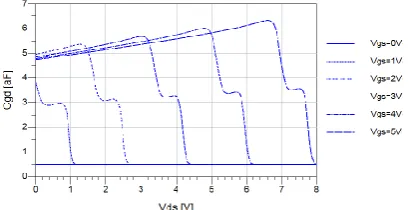
Figures 2(a) and 2(b) show the simulations of the drain and gate-source capacitances respectively in Verilog-A language [14], having assumed VFB = 0 V.
Figure 2a. Simulations of Cgd vs Vds for
Figure 2b. Simulations of Cgs vs Vds for
different values of Vgs in Verilog-A.
In SPICE we have obtained different values of Cgd and Cgs, because the
capacitance models comes from some simplifications we have adopted in the SPICE model, unlike Verilog-A implementation [8].
In the following simulations, our model has been compared with the Stanford-Source Virtual Carbon Nanotube Field-Effect Transistor model (VS-CNFET) [11-12], named by us as Wong model.
In particular this model is based on the semi-empirical virtual source concept calibrated to experimental data. The intrinsic drain current and terminal charges are based on the virtual source (VS) model, with the virtual source velocity extracted from experimental data for different channel lengths (ranging from 3-um down to 15-nm).
Moreover the VS-CNFET model takes in account the following parasitic effects:
1. direct source-to-drain and band-to-band tunneling current calibrated by numerical simulations;
2. metal-to-CNT contact resistances calibrated by experimental data; 3. parasitic capacitance including
gate-to-CNT fringe capacitances and gate-to-contact coupling capacitances.
The inputs to the VS-CNFET model are the physical device design including device dimensions, CNT diameter, gate oxide thickness, etc.
3. DYNAMIC ANALYSIS OF CNTFET LOGIC GATES
3.1. Logic Gate Parameters for Dynamic Analysis
To analyze the dynamic behavior of a logic gate, for example an inverter, the parameters of interest are the propagation delay and the rise and fall times (see Figure 3) [15].
Figure 3. Time and voltage definitions for input and output waveforms.
The rise time tr for a given signal is defined as the time required for the signal to make the transition from the 10% point to the 90% point on the waveform, during the VL-VH transition. Similarly, the fall
time tf is defined as the time required for the signal to make the transition between the 90% point and the 10% point on the waveform, during the VH-VL transition.
The 10% and 90% points are defined as follows:
V10% = VL+ 0.1∆V
V90% = VL+ 0.9∆V
where ∆V = VH – VL is the logic swing,
VH and VLare the high and low logic levels
respectively.
The propagation delay τP is defined as the difference in time between the input and output signals reaching the 50% points in their respective transitions. The 50% point is the voltage level corresponding to one-half the total transition between VH
V50% = (VH+ VL)/2
We indicate propagation delay on the high-to-low output transition with τPHL
and that of the low-to-high transition with
τPLH.
3.2 Dynamic Analysis of NOT Gate
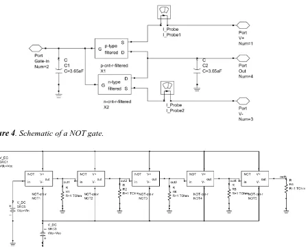
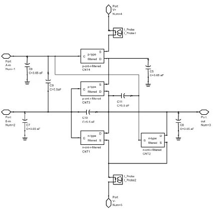
The schematic of a NOT gate implemented by Verilog-A language is shown in Figure 4.
The gate consists of two MOS-like CNTFETs with n and p channel respectively. In Figure 4 Gate-in and Out indicate the input and the output of the
gate, while V+ and V- indicate the positive and negative power supply terminals. Two current probes have been introduced to evaluate static currents flowing through the two CNTFETs.
Finally two capacitors have been introduced to model the capacitance of the metallic interconnections with respect to ground.
To perform dynamic analysis, we have used the circuit reported in Figure 5, which shows a cascade of fourNOT gates, which are internally composed as in Figure 4.
Figure 4. Schematic of a NOT gate.
Figure 5. Schematic of a cascade of four NOT gates used for transient analysis.
Parasitic capacitors have been introduced on the outputs of the gates to model the capacitance to ground of the metallic interconnections between gates. The input of the first gate is connected to an impulsive voltage generator that
provides a binary signal with high level equal to +VCC and low level equal to –VCC,
typical signal of the logic, with features similar to the output signal of the cascade. For the following simulations we use a voltage supply VCC = 0.4V, which
determines the values of the high and low logic levels. In particular we chose a simulation time equal to 80 ps that allows to view the complete waveforms at the outputs of the gates.
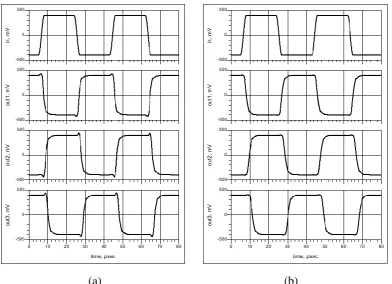
Figure 6(a) shows the result of simulation for slow transitions for the proposed model, and the same in Figure 6(b)forWong model.
In both figures we have reported outputs of the first three gates, while the fourth one works as load of the third gate.
Through these diagrams we can pull out the parameters which describe the dynamic behavior of a logic gate. In particular we determine the propagation delays and the rise and fall times for the first and third gate of the cascade, so we can observe the logic gate behavior when the input signal comes directly from the generator and when the input signal had been passed through some gates before reaching the gate in test.
(a) (b)
Figure 6.Output of the first four NOT gates and input signal vs time for slow transitions: (a) our model; (b) Wong model.
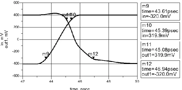
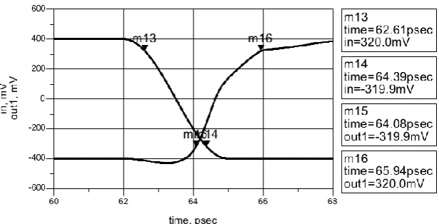
Figures 7 and 8 allow to determine the propagation delays for the high-to-low and low-to-high transitions respectively.
On these diagrams we have superposed some markers in order to determine the times corresponding to the 50% points of the transitions.
The 50% points are equal to 0 V. In this way we can easily determine the
propagation delays τPHL and τPLH, applying the definitions mentioned before. For example, for the first NOT gate we obtain: τPHL1 = tm2 - tm1 = 45.63 ps – 44.50 ps =
1.13 ps
τPLH1 = tm6 - tm5 = 64.63 ps – 63.50 ps =
Figure 7.Input and output of transients of the NOT gates for high-to-low transitions.
Figure 8.Input and output of transients of the NOT gates for low-to-high transitions.
Applying the same procedure for Wong model, we have:
τPHL1 = tm2 - tm1 = 45.97 ps – 44.50 ps =
1.47 ps
τPLH1 = tm6 - tm5 = 64.97 ps – 63.50 ps =
1.47 ps
Moreover Figures 9 and 10 allow to evaluate the rise and fall times of the input and output signals at the first NOT of the cascade, with our model.
Figure 10. Input and output of transients of the first NOT gate for low-to- high transitions.
The markers on the diagrams have been positioned at the 10% and 90% points of the level transition: in this way it is possible to determine easily the rise times tr and the fall times tf in the following way:
V10% = VL + 0.1∆V = -400 mV +
0.1∙800 mV = -320 mV
V90% = VL + 0.9∆V = -400 mV +
0.9∙800 mV = 320 mV
where ∆V = VH – VL = 400 mV – (–400
mV) = 800 mV
Corresponding to the markers, it is possible to read the times referring to these points and, therefore we can determine the rise times tr and the fall times tf. which
refer to the input and output signals. For example, for the first gate:
tr1 = tm12 - tm11 = 47.43 ps – 45.15 ps =
2.28 ps
tf1 = tm16 - tm15 = 66.43 ps – 64.15 ps
= 2.28 ps
Applying the same procedure for Wong model, we have obtained values in good agreement.
To evaluate the dynamic currents due to not instantaneous transition of the input signal of the gate, it is necessary observe that, during the level transition of the input signal, for a short time, both the CNTFETs are saturated. This happens when the signal leads the gate to the transition region. Therefore, a conducting path between the positive and negative supply exists and a certain current can flow through that path. Performing the simulation for the first NOT using our model we obtain Figure 11, while, for Wong model, we obtain the result shown in Figure 12.
Figure 12. Dynamic currents flowing through the first NOT gate (Wong model).
In both figures the n-channel CNTFET current corresponds to the first positive peak, while the p-channel CNTFET current corresponds to the first negative peak. The situation is inverted for the current peaks at 65 ps.
When the input signal at the first gate passes from the low level to the high level, the p-CNTFET turns off, whereas the n-CNTFET turns on. The load capacitance on the output of the gate, initially at high voltage level, discharges through the n-CNTFET, turned on, determining a current peak through this device which lasts for the time necessary to discharge the capacitance.
Similarly, when the input signal at the first gate passes from the high level to the low level, the n-CNTFET turns off, whereas the p-CNTFET turns on. The load capacitance starts to charge through the p-CNTFET, therefore the output passes from the initially low level to the high level, at the end of the transient. The current peak, in this case, flows through the p-CNTFET and lasts for the time necessary to charge the load capacitance.
Applying the same procedure we can perform dynamic analysis of NOT gate also for fast transitions, i.e. with reference to circuit of Figure 4, in which the input signal of the NOT cascade has rise and fall
times equal to 0.18 ps (fast transitions), high level duration of 10 ps and period equal to 20.6 ps. In this case we have obtained the rise and fall times shorter than the typical times of the logic. In order not to weigh the treatment, we limit ourselves to report the obtained results in subsequent Tables.
3.2 Dynamic Analysis of NOR Gate
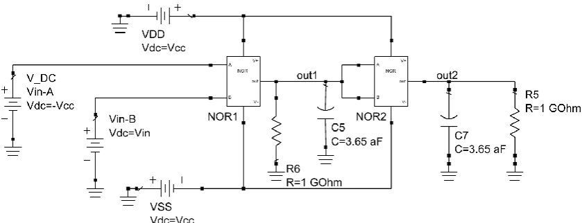
The schematic of the NOR gate is shown in Figure 13.
The gate has five terminals, that are the two inputs (A-in and B-in), the output (out) and the positive and negative supply terminals (V+ and V-).
The NOR consists of four CNTFETs (two n-channel and two p-channel), four capacitors modeling the interconnection-to-ground capacitances, three capacitors modeling the gate-to-gate and gate-to-drain parasitic capacitances of adjacent transistors and two current probes which we use to evaluate the currents flowing through the device in static or dynamic conditions.
Figure 13. Schematic of a NOR gate.
The gate-to-gate and gate-to-drain parasitic capacitances of adjacent CNTFETs have been estimated according to the value of 110 aF/μm proposed by Wong in [16]. These capacitances have a great influence to study dynamic behavior.
Similarly to the NOT case the proposed procedure has been applied to perform dynamic analysis of a NOR cascade, whose schematic is shown Figure 14.
The input of the first gate is connected to an impulsive voltage generator that provides a binary signal with high level
equal to +VCC and low level equal to –VCC,
rise time of 0.18 ps, fall time of 0.18 ps, high level duration of 52 ps and period equal to 120 ps. The rise and fall times have been chosen to give in input a typical signal of the logic, with features similar to the signals at the output of the cascade. We have chosen a power supply VCC = 0.4 V,
which determines the low and high logic levels.
Figure 14. Schematic of NOR cascade.
4. DISCUSSION OF RESULTS
The results of the transient analysis for the NOT cascade are shown in Table 1 in which the propagation delays, the rise times and the fall times of the gates of the cascade are reported.
Table 1. Results of the transient analysis of the NOT cascade, with VCC = 0.4V, for
slow transitions.
Time (ps) Our Model Wong Model
τPHL1, τPLH1 1.13 1.47
τPHL3, τPLH3 1.26 1.68
tr1, tf1 1. 86 2.28
tr2, tf2 1.98 2.55
tr3, tf3 2.00 2.57
For fast transitions the obtained results, for the first gate, are reported in Table 2.
Table 2. Results of the transient analysis of the NOT cascade for fast transitions.
Time (ps) Our Model Wong Model
τPHL1, τPLH1 0.79 1.09
tr1, tf1 1.76 2.15
The symmetrical structure of the NOT ensures that, for a certain gate, the propagation delays for high-to-low and low-to-high output transitions are equal. For the same reason, the rise times and the fall times, for a particular gate, are also equal.
The results of the transient analysis for the NOR cascade are shown in Table 3, in which we have reported the propagation delays, the rise times and the fall times of the third gate of the cascade.
Table 3. Results of the transient analysis of the NOT cascade for slow transitions.
Time (ps) Our Model Wong Model
τPHL3 3.70 4.10
τPLH3 3.90 4.80
tr3 8.90 9.90
tf3 6.10 7.10
For fast transitions the obtained results of the first gate are reported in Table 4
Table 4. Results of the transient analysis of the NOR cascade for fast transitions.
Time (ps) Our Model Wong Model
τPHL1 2.14 2.35
τPLH1 3.72 4.51
tr1 8.91 9.83
tf1 4.58 4.91
As expected, the symmetrical consideration that we have done for the NOT gate are not valid for the NOR gate.
Moreover, considering the two models, we obtained a ratio between the compilation times equal to 47.7/2.69 ≈ 17.7 and a ratio between the run times equal to 1336.42/58.84 ≈ 22.7.
5. CONCLUSIONS AND FUTURE DEVELOPMENTS
In this paper we have improved the semi-empirical compact model for CNTFETs already proposed by us, considering both the quantum capacitance effects and the sub-threshold currents, in
order to propose a procedure to study dynamic analysis of basic digital circuits. The obtained results have been compared with those of Wong model [11-12] using for this model the version downloadable on website of Stanford University, which, up today, refers to the model published in [17-18].
Actually we are working to study the effect of temperature [19-21] and of noise [22] in the CNTFET-based design of A/D circuits.
REFERENCES
1. Avouris, Ph., Radosavljević, M., Wind, S. J. (2005). “Carbon Nanotube Electronics and Optoelectronics”,
in: Rotkin SV, Subramone S, editors. Applied Physics of Carbon Nanotubes: Fundamentals of Theory, Optics and Transport Devices, Berlin Heidelberg; Springer-Verlag.
2. Perri, A. G. (2016). “Fondamenti di Dispositivi Elettronici Avanzati”, Ed. Progedit, Bari, Italy. 3. Perri, A. G. (2016). “Dispositivi Elettronici Avanzati Avanzati”, Ed. Progedit, Bari, Italy.
4. Gelao, G., Marani, R., Diana, R., Perri, A. G. (2011). “A Semi-Empirical SPICE Model for n-type Conventional CNTFETs”, IEEE Transactions on Nanotechnology, 10(3): 506-512.
5. Marani, R., Perri, A. G. (2011). “A Compact, Semi-empirical Model of Carbon Nanotube Field Effect Transistors oriented to Simulation Software”, Current Nanoscience, 7(2): 245-253.
6. Marani, R., Perri, A. G. (2012). “A DC Model of Carbon Nanotube Field Effect Transistor for CAD Applications”, International Journal of Electronics, 99(3): 427- 444.
7. Marani, R., Gelao, G., Perri, A. G. (2012). “Comparison of ABM SPICE library with Verilog-A for Compact CNTFET model implementation”, Current Nanoscience, 8(4): 556-565.
8. Marani, R., Gelao, G., Perri, A. G. (2013). “Modelling of Carbon Nanotube Field Effect Transistors oriented to SPICE software for A/D circuit design”, Microelectronics Journal, 44(1): 33-39.
9. Marani, R., Perri, A. G. (2016). “A Simulation Study of Analogue and Logic Circuits with CNTFETs”,
ECS Journal of Solid State Science and Technology, 5(6): M38-M43.
10. Marani, R., Perri, A. G. (2017). “A Study of Static Analysis in CNTFET-based Digital Circuits”, submitted to International Journal of Nanoscience and Nanotechnology.
11. Lee, C-S., Pop, E., Franklin, A.D., Haensch, W., Wong, H.-S. P. (2015). “A Compact Virtual-Source Model for CarbonNanotube FETs in the Sub-10-nmRegime—Part I: Intrinsic Elements”,.IEEE Transactions on Electron Devices, 62(9): 3061-3069.
12. Lee, C-S., Pop, E., Franklin, A. D., Haensch, W., Wong, H.-S. P. (2015). “A Compact Virtual-Source Model for Carbon Nanotube FETs in the Sub-10-nm Regime—Part II: Extrinsic Elements, Performance Assessment, and Design Optimization”,. IEEE Transactions on Electron Devices, 62(9): 3070-3078. 13. Marani, R., Perri, A. G. (2016). “Analysis of CNTFETs Operating in SubThreshold Region for Low Power
Digital Applications”, ECS Journal of Solid State Science and Technology, 5(2): M1-M4. 14. Verilog-AMS language reference manual, Version 2.2, Accellera International, Inc., (2006).
15. Marani, R., Perri, A. G. (2017). “CNTFET Electronics: Design Principles”, Ed. Progedit, Bari, Italy, ISBN
978-88-6194-307-0.
16. Luo, J., Wei, L., Lee, C-S., Guam, X., Pop, E., Antoniadis, A., Wong, H.-S. P. (2013). “Compact Model for Carbon Nanotube Field-Effect Transistors Including Nonidealities and Calibrated With Experimental Data Down to 9-nm Gate Length”, IEEE Transactions on Electron Devices, 60(6): 1834-1843.
17. Deng, J., Wong, H.-S. P. (2007). “A Compact SPICE Model for Carbon-Nanotube Field-Effect Transistors Including Nonidealities and Its Application—Part I: Model of the Intrinsic Channel Region”,.IEEE Transactions on Electron Devices, 54(12): 3186-3194.
18. Deng, J., Wong, H.-S. P. (2007). “A Compact SPICE Model for Carbon-Nanotube Field-Effect Transistors Including Nonidealities and Its Application—Part II: Full Device Model and Circuit Performance Benchmarking”, IEEE Transactions on Electron Devices, 54(12): 3195-3205.
20. Marani, R., Perri, A. G. (2016). “A DC Thermal Model of Carbon Nanotube Field Effect Transistors for CAD Applications”, ECS Journal of Solid State Science and Technology, 5(8): M3001-M3004.
21. Marani, R., Perri, A. G. (2017). “Effects of Temperature Dependence of Energy Band Gap on I-V Characteristics in CNTFETs Models”, International Journal of Nanoscience, 16(05n06).
![Figure 3) [15].](https://thumb-us.123doks.com/thumbv2/123dok_us/1310857.1638673/3.595.331.513.180.410/figure.webp)