Article
Non-Invasive Detection Method for Recycled Flash
Memory using Timing Characteristics
Sadman Sakib , Preeti Kumari, B. M. S. Bahar Talukder, Md Tauhidur Rahman, and Biswajit Ray*
Department of Electrical and Computer Engineering, The University of Alabama in Huntsville, AL 35899, USA; {ms0171, pk0039, bt0034, tauhidur.rahman, and biswajit.ray}@uah.edu
* Correspondence: [email protected]; Tel.: +1-256-824-5679
† This paper is an extended version of our paper published in 2018 IEEE International Symposium on Hardware Oriented Security and Trust (HOST), Washington, DC, USA, 2018; pp. 89-95, DOI: https://doi.org/10.1109/HST.2018.8383895.
1 2 3 4 5 6 7 8 9 10 11 12
Abstract: Counterfeitingelectroniccomponentsisaseriousproblemforthesecurityandreliability of any electronicsystems. Unfortunately, thenumber of counterfeit componentshasincreased considerably aftertheintroductionof horizontalsemiconductorsupplychain. Inthispaper,we proposeanewmethodfordetectingrecycledFlashmemory,amajortargetofthecounterfeiters duetoitsubiquitoususage.ProposedmethodisbasedonmeasurementofchangeinFlasharray characteristics(suchaserasetime,programtime,failbitcount,etc.)withitsusage.Wefindthaterase timeisthebestmetrictodistinguishausedFlashchipfromafreshoneforthefollowingreasons:(1) erasetimeshowsminimalvariationamongdifferentfreshmemoryblocks/chipand(2)erasetime increasessignificantlywithusage.Weverifyourmethodforawiderangeofcommercialofftheshelf Flashchipsfromseveralvendors,technologynodes,storagedensityandstoragetype(single-bitper cellandmulti-bitpercell).Theminimumdetectablechipusagevariesfrom0.05%to3.0%ofitstotal lifetimedependingontheexactdetailsofthechip.
Keywords: Counterfeiting;recycledFlashmemory;recycledFlashmemorydetection 13
1. Introduction 14
Counterfeit electronics have become a significant concern in the globalized semiconductor 15
industry where chips might be recycled, remarked, cloned, out-of-spec/defective, and tampered 16
[1–5]. Flash memory, which is commonly used as non-volatile data storage in many electronic systems, 17
is one of the primary targets of the counterfeiters [6]. Counterfeiting of Flash memory has the severe 18
consequence of its reliability or lifetime due to its limited endurance. The endurance of Flash is critical 19
in many embedded applications where Flash is used for storing the operating system or other sensitive 20
information. Hence the failure of Flash memory essentially leads to system failure, which might have 21
a radical impact on many critical applications including healthcare, aero-space, defense, etc. In this 22
context, use of recycled or fake Flash memories in critical areas may cause loss, not limiting to resources 23
but to human life as well. Therefore, it’s vital to prevent these recycled memories entering into the IC 24
supply chain. 25
Identification of counterfeit Flash memory with non-invasive technique is extremely difficult as 26
the memory chip may remain functional at the time of selling a product and hence it may pass the 27
standard product qualification tests. In addition, there remains chip-to-chip manufacturing variation, 28
which makes the early stage detection of counterfeit Flash memory even harder with the standard 29
test solutions. While there are several recent research in the area of counterfeit IC detection (details 30
given in section3), most of the existing techniques suffer from following major limitations: (i) requires 31
hardware modification in the design phase, (ii) requires maintenance of large database, (iii) produces a 32
large number of false positive results, (iv) time consuming and manual labor extensive etc. In general, 33
detection of recycled Flash memories must follow the following criteria [4,5,14]: 34
2 of 13
• The detection techniques of recycled memory have to be quick, non-destructive, and inexpensive. 35
• The techniques must support detection of mass-volume chips. The ID-based approach is complex 36
and not suitable for mass-volume detection. 37
• The detection mechanism must support existing memory and new memory. Sensor-based 38
approaches only work for newly fabricated chips. 39
• The detection mechanism has to be straightforward and vendor-independent. The detection 40
techniques have to be robust to environmental variations (voltage and temperature variation). 41
• The detection mechanism should have no or a minimal usage of the database. 42
• The detection mechanisms must have a very high level of confidence. 43
• The proposed techniques must provide yes-no decision. These techniques need to be able to tell 44
the exact usage of the memory too. 45
• The proposed techniques should be independent of the vendor, technology node, and capacity. 46
However, the threshold of detection parameter might vary across manufacturers, technology 47
nodes, and capacities. 48
In this paper, we propose a method that satisfies the above detection criteria. The major 49
contributions of this article include: 50
• We propose a comprehensive framework to detect used Flash memories by measuring the Flash 51
array characteristics, such as erase time, program time, fail bit counts, etc. 52
• Experimental data shows that erase time is the best metric to detect recycled Flash chip. We find 53
that erase time shows minimum variation between different memory blocks and it increases 54
significantly with usage. 55
• We validate our proposed method with commercial off the shelf Flash chips from several vendors, 56
technology nodes, memory type (SLC vs. MLC), and capacity (i.e., memory size). Measurement 57
results show that we can detect a recycled Flash chip with high accuracy if it has been used as 58
less as 0.05% to 3.0% of its total lifetime. 59
• Proposed method does not require any hardware modification or any prior database maintenance. 60
Hence it can be implemented on many existing storage solution with system updates. 61
The rest of the paper is organized as follows. In Section2, we describe the details of Flash memory 62
and the metrics of our interest to characterize recycled Flash memory. The existing work in the area 63
of detecting counterfeit IC is discussed in Section3. The characterization of Flash memory and our 64
proposed method to detect recycled Flash memory are described in Section4. Section5will provide 65
the results of our experimental test setup. We conclude our work in Section6. 66
2. Background 67
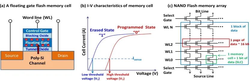
Flash Memory Cell:The device structure of a single Flash memory cell is shown in Fig.1(a). It is 68
essentially a Metal-Oxide-Semiconductor Field Effect Transistor (MOSFET) with a floating gate (FG) in 69
the oxide layer. The floating gate can hold charge (electrons) for a long time even in the absence of 70
any voltage on the control gate.The floating gate is typically made of poly-Si or Si-nitride (charge trap 71
layer). As shown in Fig. 1, there are two important insulating layers in the device structure: one is 72
called tunnel oxide which insulates the floating gate from the transistor channel. The other insulating 73
layer is called blocking oxide which isolates the control gate from the floating gate. Information or 74
binary bits are stored in the form of electric charges on the floating gate. 75
Flash Memory Array:The memory cells or FG transistors are organized in a NAND Flash chip 76
as multiple two-dimensional arrays known as Flash blocks as shown in Fig.1(c). The cells in each row 77
of a block are electrically connected through a single Word Line (WL), which acts as the control gate of 78
individual FG transistors. Each column of cells in a block is connected to a different Bit Line (BL). The 79
number of cells in each row defines the size of a page, which is typically 8-16k Byte in size. As shown 80
in Fig.1, each block consists of multiple WLs (typically 32-128 WLs per block) which correspond to 81
different page addresses. For single-level cell (SLC) technology, each WL defines one page (or two 82
3 of 13
Poly-Si Channel
Source
Tunnel Oxide Floating Gate
-Blocking Oxide
Drain
Control Gate
Word line (WL)
Voltage (V)
Cel
l C
ur
ren
t (
A
)
Isense
Erased State “1”
Programmed State “0”
High threshold voltage (VT) Low threshold
voltage (VT)
(a) A floating gate flash memory cell (b) I-V characteristics of memory cell (c) NAND Flash memory array
WL0 WL1 WL2 WL N Select Gate
Select Gate
Bit Line
1 block of data
1 memory cell = 1 bit of data (SLC)
Source Line
1 page of data ~ 16 kB
Figure 1.(a) A floating gate NAND Flash memory cell which stores charge in the floating gate (or charge trap layer). Metal word-line (WL) of the array is connected to the control gate. Electron tunneling takes place through tunnel oxide from transistor channel to FG. Blocking oxide prevents back tunneling of stored charge to control gate. (b) Typical current-voltage characteristics of the memory cell. (c) The hierarchical storage in NAND Flash array consisting of kilo-bytes of memory cells connected through a single WL (called a page of information). A group of WL forms a block of memory. The select gate transistors can be standard MOSFET or floating gate transistors, depending on manufacturers or technology node.
pages by grouping even bits and odd bits). For multi-level cell (MLC) technology, each WL defines at 83
least two pages of data. Read and program operations are performed for one page at a time, while 84
erase is performed on the entire block. 85
Flash Memory Operation:Flash memory offers three basic operations: program, erase and read. 86
During a program operation, charges are injected into the floating gate from the transistor channel 87
by Fowler-Nordheim tunneling through the tunnel oxide. Typically, multiple pulses of high voltage 88
are needed on the control gate of the cell during programming. After programming, electron density 89
or negative charges rises on the floating gate, increasing the threshold voltage of the FG-MOSFET. 90
This programmed state of the memory cell represents the binary bit "0" in single bit per cell (SLC) 91
technology. The cells are erased by applying a high positive voltage on the substrate of the transistors 92
while the control gate voltage is grounded. This reverses the electric field directly across the tunnel 93
oxide forcing the electrons tunneled out of the floating gate into the transistor channel. This erased 94
state will have lowerVT, and it represents logic "1" in binary bit representation. Read operation in
95
Flash memory involves sensing the threshold voltage (VT) of floating gate transistors. As shown in Fig.
96
1(b),VTof the transistor depends on the current-voltage characteristics, where a fixed sense current
97
(Isense) is usually used to determine the exactVT. During a read operation, a fixed "read reference
98
voltage" (Vre f), which is lower than the programmed voltage, is applied to the control gate. Based on
99
theVTof the transistor, the cell will conduct current or not, and this will be sensed as bit "1" or "0"
100
respectively, by the sense circuitry of the Flash memory. 101
3. Existing Work on Detecting Counterfeit IC 102
Over the past few years researchers have proposed several methods to detect counterfeit ICs, 103
which can be classified into four groups: 1) physical and electrical tests, 2) track and trace, 3) data 104
analysis, and 4) aging sensors. Physical tests are invasive in nature as they are based on probing any 105
physical modification of counterfeit ICs. Electrical tests can be used to detect defects and anomalies like 106
broken/missing bond wires, open/short interconnect etc. and find the defects and anomalies related 107
to the internal structures, and logic gates [5,11]. Another test method is tracking and tracing, where IP 108
watermarking, IC metering or hardware metering are used to detect the counterfeit ICs [25–28]. Aging 109
sensors can be implemented to monitor and realize the aging and reliability of electronic components. 110
4 of 13
have been proposed to sense the age of ICs: [29] measure the beat frequency of two ring oscillators 112
(stressed and unstressed), [30] used NBTI and defect-induced oxide breakdown effect, [31] detected 113
the performance degradation of an aged MOSFET through threshold voltage detector. Sensor-based 114
approaches are promising, but they need additional hardware and hence not applicable to the existing 115
electronic chips. The image-based technique is another solution to detect counterfeit ICs but requires 116
expensive image acquisition infrastructure and often suffers from high computational complexity. 117
SVM has been used to identify whether a chip is authentic or not. However, it involves a collection of 118
a set of parametric measurements and a trusted party to collect those data [21]. In [10], the path-delay 119
fingerprinting technique is presented to differentiate recycled ICs from genuine ones through changes 120
in their path-delay distribution caused by prior usage. However, this technique requires data from 121
genuine ICs, which makes it impractical. 122
Concerning fake Flash detection, Guo et al. in [6], used partial programming concept to detect the 123
recycled Flash memory for more than 5% of its end-of-life usage. However, their technique is time 124
intensive and requires maintenance of extensive database, which limits its applicability for wide range 125
of products. In [7–9], an ID-based approach was proposed to detect recycled SRAM chips. In this 126
method, the startup values of an SRAM memory are used to create the device signatures. The signature 127
is generated in such a way that the degradation due to aging shows up in the signature. The recycled 128
SRAM chips can be identified by comparing the signature of fresh SRAM chip with the signature of 129
SRAM chip under test. In this method, the high and the low temperature need to be applied to select 130
perfect SRAM cells to generate a signature which is costly to perform and not suitable for high-volume 131
detection. The existing works are mostly on FPGA, SRAM, DRAM etc. and they are expensive, time 132
consuming, some of them are ineffective due to process variations and environmental variations in 133
lower technology nodes and low confidence of identifying recycled ICs [5,11,32]. There are very few 134
work on the detection of recycled Flash memory. 135
4. Recycled Flash Memory Detection 136
In this section, we present our framework for recycled Flash chip detection in detail by analyzing 137
memory characteristics as a function of chip usage. Specifically, we analyze the impact of program-erase 138
(PE) cycle count (which is the indication of chip usage) on program completion time for a page, erase 139
completion time for a block and fail bit count (FBC) per page. 140
The aim of this study is to identify the appropriate Flash characteristics which can be used as the 141
best indicator of its usage in order to distinguish a recycled memory chip from a fresh one with high 142
accuracy. As discussed in the background section of Flash memory, both program and erase operation 143
involves high voltage either on control gate (during the program) or on the Si substrate (during erase). 144
Application of high voltage exerts high field stress across the tunnel oxide of the Flash memory cell 145
and creates defects in the oxide as well as at the interface between oxide and silicon (Si) channel. The 146
more is the PE cycle count; more is the defect creation. The key impact of the defects is the reduction of 147
electric field across the oxide which slows down the erase operation. The program operation slightly 148
gets faster due to the increase in the cell threshold voltage caused by defects. Even though program 149
speed typically increases with PE cycle count, it also increases the probability of over-programming 150
which increases the fail bit count in a page after the program. Also, the read noise increases with the 151
creation of defects in the Si-channel interfaces which will cause fluctuation in the cell current during 152
sensing resulting in increased FBC [24]. In subsection5.3, we monitor erase time, program time and 153
FBC as a function of PE cycle count to formulate a framework for recycled Flash chip detection. 154
One of the main challenges for the recycled Flash chip detection is to account for the manufacturing 155
variation existing between the different chip of the same technology as well as variation existing among 156
different blocks of the same chip itself. For accurate identification of recycled chip, we need to ensure 157
that there is no overlap in the distribution of the identified device property between a fresh chip and a 158
used chip. Thus we need to identify an appropriate memory characteristic, which is easily measurable 159
and has a distinguishable change in its value with PE cycling. 160
5 of 13
(b)
Confidence Level Plot
1
α
0α
1Flash Parameter (e.g. erase time)
Pr
o
ba
bility
Usage (%)
Co
nfidence
Lev
el
(%
)
Us
age
–
u
2%
Usage
–
u
1%
(1-α1)*100
(1-α2)* 100
100
(a)
Us
age
–
u
n%
Figure 2. (a) The CDF of decision parameters changes with usage and (b) the confidence level calculation from the CDF. Confidence level changes with usage.
Fig.2shows our recycled Flash identification approach. We measure several Flash characteristics 161
(such as erase time) on different memory location of a chip in order to plot the variation of that 162
parameter within a chip. Then, we compare the same Flash characteristics as a function of memory 163
usage as shown in Fig. 2(a). The figure shows that the upper tail (CDF) of Usage-0% intersects 164
the lower tail (CDF) of Usage-u1% atα1, so the confidence level to detectu1% usage is (1 -α1) * 100.
165
Whereas, the intersection point (α2) for Usage-0% and Usage-u2%, isα2= 0 and so, the confidence
166
level to detect a recycled Flash memory is∼100%, when the Flash memory is used foru2% of their
167
lifetime. Here, Alpha (α) defines the cumulative probability of the used chip to fall below the threshold 168
of detection (Flash) parameter. From the value ofα, we can compute the confidence level, which 169
measures whether we can detect a recycled memory accurately. Fig.2(b) shows the confidence level 170
which can be obtained from Equation (1). 171
Con f idence level= (1−α)∗100% (1)
A 100% confidence means that a counterfeit Flash memory is identified as a counterfeit one. From 172
Fig.2(b), we can conclude that we can only detect those used chips which have been used foru2%
173
of their lifetime where the confidence level is 100%. If the chip has been used for less thanu2% of
174
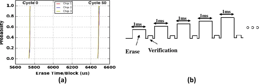
endurance then we cannot decide whether the chip is used or fresh. Fig.3(a) shows our experimental 175
result for erase time distribution on MLC chip. We find that, there is no overlap in the distribution 176
between fresh and used chip (50 times PE cycled). This means, 50 times cycled chip can be detected 177
with high accuracy by monitoring erase time. The increase in erase time is monotonic with PE cycle 178
count as verified from the data discussed in the next section. In general, there should not be any 179
overlap between the fresh CDF and the used CDF of PE cycle for the high confidence level. However, 180
there might be an overlap between the distributions (i.e., fresh vs. used CDF) because of low usage of 181
a chip, which can reduce the confidence level. Therefore, in our experiment,≥98% confidence level is 182
considered as an acceptable confidence level to conclude whether the chip under test is recycled or 183
6 of 13
Erase Operation
Erase Verification
1ms
1ms 1ms
1ms 1ms
1ms
(a)
(b)
Figure 3. (a) Used vs. fresh Flash memory: timing characteristics change over time. (b) The erase operation in the NAND Flash takes place in multiple pulses or loops.
5. Results and Analysis 185
5.1. Experimental Set-up 186
Results reported here are based on data collected from off the shelf Flash chips (see Table2for the 187
specifications). We use a custom design board to program, erase, and read the Flash chips. The board 188
contains a socket to hold a Flash chip under test, an ARM microprocessor to issue commands and 189
receive data from the Flash chip and a serial interface. A summary of steps followed for data collection 190
in our experiment is explained below: 191
• Initially a block is selected on which we want to perform program erase function. 192
• The selected block is then erased, or in other words, all the bits of that block are "1". 193
• Then the block is programmed with All "0" data pattern. 194
• Read operation is then performed on one page at a time. 195
• Program time, Erase time and FBC are then recorded. 196
• Process is then continued for other blocks of the chip. 197
• Finally different plots are obtained by analyzing the recorded data. 198
In our experiment, we used 100 blocks per chip and performed the same analysis as a function of 199
PE cycle count. All the blocks after programming should have all bits "0", but it is observed that few 200
bits flip and those are called as fail bits. We count the number of fail bits per page which we call FBC 201
(fail bit count). The behavior of erase and program time are analyzed for different PE cycle count. We 202
perform our analysis on the different type of Flash chips (SLC and MLC) from various manufacturers 203
of different technology nodes. 204
5.2. Measurement Procedure for Flash Timing 205
To measure the Flash timing characteristics such as erase time, we first measure the time (tstart)
at which the erase command is issued by a microcontroller. We again measure the time (tend) after
completion of erase operation. The time difference between (tend) and (tstart) is the erase time (tend
-tstart) used in this work.
Erase time(terase) =tend−tstart (2)
Erase operation (Fig.3(b)) in Flash memories happens in multiple pulses (pulse width∼1 ms). 206
After every pulse, a verify operation is applied to check the state of all the cells. If the cells are not 207
erased, then another pulse and verify operation is applied. This process will continue until all the cells 208
get erased. Such type of pulse by pulse erasing is the reason for the step-wise increase in erase time. 209
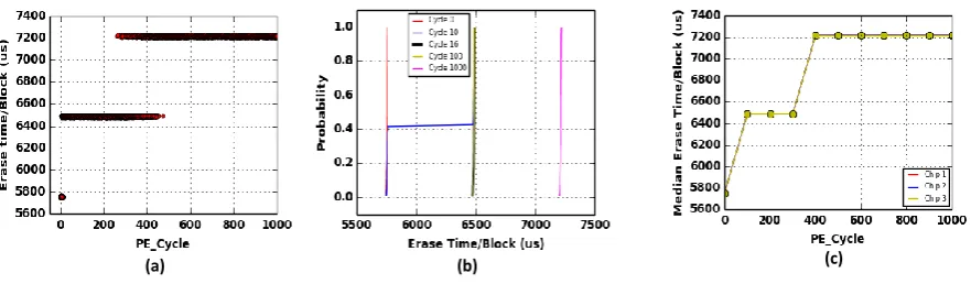
Fig.4(a) shows that the erase time increases in steps. 210
7 of 13
(a) (b) (c)
Figure 4.(a) Scatter plot of erase time (Y-axis) with respect to program erase cycles (X-axis). For each PE cycle count, we have used 100 blocks to obtain the scatter plot, (b) Cumulative Distribution Function (CDF) of Erase time for cycle 0, 10, 16, 100, and 1000, and (c) Median erase time per block (Y-axis) with respect to PE cycle count (X-axis).
5.3. Evaluation of Different Flash Characteristics for Early Detection 211
In this section, we provide data for different memory performance parameters (erase time per 212
block, program time per page, fail bit count per page, etc.) as a function of PE cycling. Fig.4(a) shows 213
the erase time dependence on PE cycle count. Note that erase time increases with cycling in discrete 214
steps. Such step by step increase of erase time is a result of pulse by pulse erase operation as described 215
in Fig.3(b). Fig.4(a) also shows an overlap region, where two different erase time is observed for 216
a given PE cycle count. This is due to the block to block variation in erase time degradation with 217
cycling. In our experiment we choose 100 blocks for every PE cycle count and the overlap region 218
shows that different block has different erase time. Block to block variability is more clearly illustrated 219
in Fig.4(b), where the cumulative distribution of erase time is plotted for a given PE cycle condition. 220
Interestingly, we find that erase time has a very sharp distribution (or minimal variation) for fresh 221
condition (red). However, with few PE cycle erase time distribution widens (blue). This imposes a 222
constrain on minimum usage detection threshold, since for accurate detection of cycled condition there 223
should not be any overlap between fresh and cycled distribution. With the Micron MLC chip we find 224
that for PE cycle count = 16, erase time distribution has no overlap with fresh (black curve) condition. 225
Thus, minimum usage that can be detected with erase time for this chip = 0.32% (end of life PE cycle 226
count = 5000). In Fig.4(c) we show the erase time dependence on PE cycling for 3 different chips of 227
the same part number, which shows minimal chip-to-chip variation and hence the applicability of the 228
erase time based detection method. 229
In Fig.5(a), we show the program time dependence on PE cycle count. The results show that 230
the value of program time is decreasing with the number of program-erase cycle. The reduction of 231
program time is expected from a Flash memory chip, as with higher PE cycles the threshold voltage of 232
the individual cells slightly increases due to decreasing in the cell current caused by defect creation in 233
the Si-oxide interfaces. However, as shown in Fig.5(b), the cumulative distribution of program time is 234
wider, and it overlaps with the program time distribution of cycled blocks. Thus, program time alone 235
cannot distinguish fresh and cycled blocks with∼100% accuracy. To confirm the identical behavior 236
from different chips, we plot the similar program time data from three other chips in Fig.5(c) and the 237
plot shows identical behaviors among the chip. 238
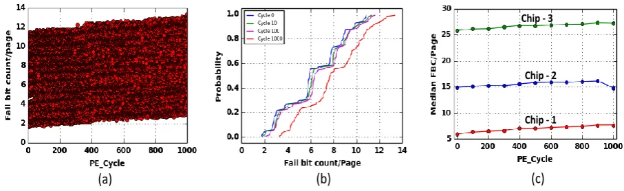
In Fig. 6(a), we plot the FBC of a page just after programming that page as a function of PE 239
cycle count. We took 100 blocks and program-erase them for 1000 cycles, and plotted the scatter plots 240
for all the values of FBC per page. As expected, the value of FBC is increasing with the number of 241
program-erase cycle. However, the CDF plot for the FBC shows wider distribution and strong overlap 242
8 of 13
(a) (b) (c)
Figure 5.(a) Scatter plot of program time (Y-axis) with respect to program erase cycles (X-axis). This is the scatter plot for the output of program time of 100 blocks, program-erased for 1000 cycles. (b) Cumulative Distribution Function (CDF) of program time for cycle 0, 10, 100, and 1000. (c) Median program time per page (Y-axis) with respect to PE cycle count (X-axis).
Micron MLC 64GB – Fail Bit Count Plot – Scatter, CDF,
Median
Chip - 1 Chip - 2 Chip - 3
(a)
(b)
(c)
Figure 6.(a) Scatter plot of fail bit count (Y-axis) with respect to program-erase cycles (X-axis). This is the scatter plot for the output of fail bits of 100 blocks, program-erased for 1000 cycles, (b) Cumulative Distribution Function (CDF) of FBC for different PE cycle counts, and (c) Median FBC per page (Y-axis) with respect to PE cycle count (X-axis).
chip. To confirm the identical behavior among different chip of the same part number, we plot the 244
similar FBC data from three other chips in Fig.6(c) and the plot shows identical behaviors among the 245
chip. 246
In summary, experimental data shows that erase time is the best metric in order to distinguish 247
a recycled Flash chip from the fresh one for the following reasons: 1) Erase time has very tight 248
distribution (or minimal variation) on a fresh chip. Thus, the median erase time typically specified in 249
the product data sheet is a good representation of erase time value for that class of Flash ICs, 2) With 250
program erase cycling, erase time increases in discrete but large steps (∼1 ms). The large increase 251
in erase time with usage and the initial tight distribution ensures that there is no overlap of erase 252
time distribution of a fresh chip vs used chip, 3) The minimum usage level for accurate detection of 253
used chip using erase time will depend on the exact technology and chip details, however, the general 254
methodology will hold for any Flash chip. 255
5.4. Validation on Different Technology Nodes 256
We find that the proposed method works for different technology nodes. We validated our 257
proposed technique with two 8GB SLC Flash memory chips from the same manufacturer of different 258
technology nodes (34nm and 25nm). Fig.7(a) and7(b) present that the erase time CDF for 34nm and 259
9 of 13
Cycle - 50
Cycle - 1100
Cycle - 1500
Cycle - 2000 Cyc
le
-2700
Cyc
le
-0
Cycle - 6 Cycl
e
-20
Cycle - 30
Cycle - 40
Cycle - 50
Cyc
le
-67
(a)
(b)
(c)
Figure 7.(a) CDF of erase time for PE cycle 0, 50, 1100, 1500, 2000 and 2700 for Micron 8GB SLC (34nm). (b) CDF of erase time for PE cycle 6, 20, 30, 40, 50 and 67 for Micron 8GB SLC (25nm). (c) The confidence level for the Flash chips of 34nm and 25nm technology node.
Cycle - 50
Cycle - 1100
Cycle - 1500
Cycle - 2000 Cyc
le
-2700
Cyc
le
-0 Cycle-1700
Cycl
e
-0
&
500
Cyc
le
-2000
Cycle-1600
Cycle-1850
(a)
(b)
(c)
Figure 8.(a) CDF of erase time for PE cycle 0, 50, 1100, 1500, 2000 and 2700 for Micron 8GB SLC (34nm). (b) CDF of erase time for PE cycle 0, 500, 1600, 1700, 1850 and 2000 for Toshiba 8GB SLC (32nm). (c) The confidence level for the Flash chips from two manufacturers, Micron and Toshiba.
25nm technology nodes. The results show that the erase time increases as the number of PE cycles 260
increases. We also find that the Flash chips from different technology nodes degrade at different rates. 261
The degradation rate is faster for a smaller technology node compared to an older technology node. As 262
the technology node is scaled down, the number of electron/cell decreases. As cell size reduces, small 263
number of defects created by few program-erase cycles will cause large positive shift in the intrinsic 264
threshold voltage of the cells. Therefore, it becomes harder to erase cells of lower technology nodes 265
after a few cycles of usage. For 34nm technology node (Fig.7(a)), the erase time changes after usage 266
of 2700 PE cycles. A change in erase time is observed after only 67 PE cycles for the 25nm technology 267
node. The usage vs. confidence level plot in Fig.7(c) shows that a Flash chip of lower technology node 268
(25nm) can be detected at earlier (usage 0.05% for the sampled chips) stage than a higher technology 269
node (usage 2.7% for the sampled chips). Table2shows more results and comparison from different 270
technology nodes for a given manufacturer. 271
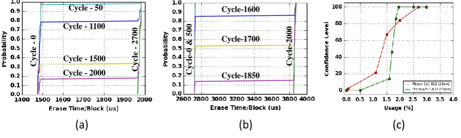
5.5. Validation on Flash Chip from Different Manufacturers 272
Another important criterion of a detection methodology is that it has to be independent of 273
manufacturers. Here we validate our method using two SLC Flash memories from two important 274
manufacturers, Micron and Toshiba. Fig.8(a) and8(b) show the CDF plot for the erase time for Micron 275
and Toshiba respectively at different PE cycles. The experimental data shows that Micron and Toshiba 276
10 of 13
Cycle - 50
Cycle - 1100
Cycle - 1500
Cycle - 2000 Cyc
le
-2700
Cyc
le
-0
Cyc
le
-0
Cycle - 33
Cycle – 41
Cycle - 47
Cycle - 58
Cyc
le
-70
(a)
(b)
(c)
Figure 9. (a) CDF of erase time for PE cycle 0, 50, 1100, 1500, 2000 and 2700 for Micron 8GB SLC (34nm). (b) CDF of erase time for PE cycle 0, 33, 41, 47, 58 and 70 for Micron 32GB MLC (20nm). (c) The confidence level for two types Flash chips – SLC and MLC.
shows the usage vs. confidence level plot for Micron and Toshiba Flash chips. The results conclude that 278
our proposed method can detect whether a Flash chip is recycled or not with an acceptable confidence 279
level. Table2shows more results and comparison from the major manufacturer. 280
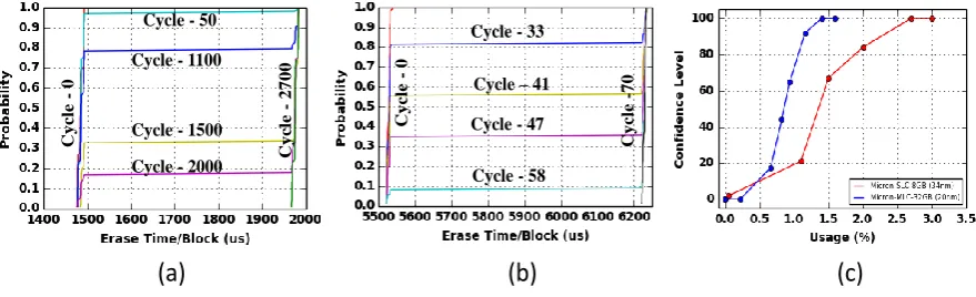
5.6. Validation on SLC and MLC Flash Chips 281
We applied our proposed method on both SLC and MLC Flash types from the same manufacturer. 282
Fig.9(a) and9(b) shows the same trend for the erase operation (i.e., increase in erase time with the 283
number of PE cycles). The erase time increasing rate is much faster in MLC Flash chip than the SLC 284
Flash chip. From Fig. 9, we can see that the SLC Flash chip can be identified after 2700 PE cycles, 285
whereas the counterfeit MLC Flash chip requires only 70 PE cycles. The density of MLC is much higher 286
than SLC because of MLC store two or more bits per cell, whereas SLC stores only one bit per cell. 287
Also, the MLC Flash chip has a wider range of voltage, typically 0V to 6V, while the SLC has lower 288
voltage range (0V to 3V). Hence, the MLC degrades faster and offer very early age detection compared 289
to SLC. 290
5.7. Usage vs. Confidence Level 291
Table1shows that the confidence level or the accuracy of detecting recycled Flash chips increases 292
with usage. We can see the same trend for various Flash chips from different manufacturers, different 293
technology nodes, types, etc. The results show that we can not conclude whether the chip is recycled 294
or not for all three vendors when the chips are used for 1% and 1.4% of their lifetime. However, 295
vendor 1 and vendor 2 can be detected if the chip is used for 2% of their lifetime. We can not make any 296
conclusion for the 3rd vendor because the confidence level is not acceptable at 2% of usage. For usage 297
of 2.7%, we can identify recycled chips for all three vendors. We can conclude that a recycled Flash 298
chip can be detected with a better confidence level if that particular chip degrades faster. 299
Table 1.The confidence level for different types of Flash chips from various manufacturers
Usage (%) Confidence Level
Vendor 1 Vendor 2 Vendor 3
1% Not Acceptable Not Acceptable Not Acceptable 1.4% Acceptable Not Acceptable Not Acceptable 2% Acceptable Acceptable Not Acceptable
2.7% Acceptable Acceptable Acceptable
*Acceptable (i.e.,≥98% confidence level)
11 of 13
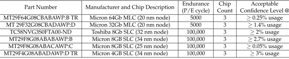
Table 2.Summary of results for the different type of Flash chips
Part Number Manufacturer and Chip Description Endurance (P/E cycle)
Chip Count
Acceptable Confidence Level @ MT29F64G08CBABAWP:B TR Micron 64Gb MLC (20 nm node) 5000 3 ≥0.25% usage
MT 29F32G08CBADAWP:D Micron 32Gb MLC (20 nm node) 5000 3 ≥1.4% usage TC58NVG3S0FTA00-ND Toshiba 8Gb SLC (32 nm node) 100,000 3 ≥2% usage MT29F8G08ABABAWP:B Micron 8GB SLC (34 nm node) 100,000 3 ≥2.7% usage MT29F8G08ABACAWP:C Micron 8GB SLC (25 nm node) 100,000 3 ≥0.05% usage MT29F4G08ABADAWP:D TR Micron 4GB SLC (34 nm node) 100,000 3 ≥3% usage
*Acceptable (i.e.,≥98% confidence level)
Summary of results for the different type of Flash chips:Table2, Fig.7,8, and9present the summary 300
of results for the different type of Flash chips from various manufacturers of different technology nodes, 301
types (SLC vs. MLC), and capacities. The results show that MLC Flash chips can be detected much 302
earlier than SLC Flash chips from the same manufacturer. In general, the degradation of MLC chips is 303
quicker than SLC because the operating voltage of MLC is higher. In another case, the Flash chips from 304
different technology nodes from the same manufacturer degrade at different rates. The result shows 305
that a Flash chip of lower technology node can be detected earlier than the older technology node. The 306
reason for such trend is mostly due to the smaller size and lower gate oxide thickness of the memory 307
cells in lower technology nodes. The results also conclude that the proposed detection methodology 308
works for different manufacturers and recycled Flash chip can be detected with acceptable confidence 309
level. 310
Summary of Results: 311
• Timing analysis confirms that erase time distribution can be used to distinguish between a fresh 312
and recycled chip at acceptable accuracy. 313
• How early a Flash chip can be detected (i.e., the ’usage’ ) with acceptable confidence depends on 314
manufacturers, technology nodes, memory types (SLC vs. MLC), and capacity. 315
• Erase time is the best Flash parameters to detect a used chip as early as possible (i.e., with 316
minimal usage). FBC and program time also show changes over time but not good enough to 317
detect recycled Flash chip with minimal usage. 318
Limitations and Scopes of Future Work: 319
• Impact of Testing on Wear-out:Our technique involves one erase operation per block, which 320
have minimal impact on aging (typical erase count for a chip is∼100,000). 321
• Test Time:Testing entire chip can take few seconds because typical erase operation take 1 to 10 322
milliseconds per block and a chip can contain more than 1000 blocks. 323
• Temperature Effect:Our methodology works for all different temperature, however the exact 324
detection threshold depends on operating temperature. 325
6. Conclusion 326
Recycled Flash memory is a major threat to any electronic systems, from critical (e.g., military 327
applications) to non-critical consumer electronic systems. In this paper, we proposed a non-invasive 328
framework to detect used Flash memories from the fresh ones, with the help of timing characteristics 329
of memory (Program time, Erase time) and the number of faulty bits. Experimental results show 330
that our framework performs with high accuracy without requiring any prior database. We find 331
that the minimum detectable usage depends on the manufacturers, technology nodes, types (SLC vs. 332
MLC), and capacity. Our proposed methodology is inexpensive, non-destructive, and does not require 333
any hardware modification or maintenance of extensive database apart from the standard product 334
12 of 13
References 336
1. Karri, R; Koushanfar, F. Trustworthy Hardware [Scanning the Issue]. In Proceedings of the IEEE,Aug. 2014, 337
102, pp. 1123-1125. 338
2. Fern, N.; San, I.; Koç, Ç. K.; Cheng, K. T. T. Hiding Hardware Trojan Communication Channels in Partially 339
Specified SoC Bus Functionality. In IEEE Transactions on Computer-Aided Design of Integrated Circuits and 340
Systems,Sept. 2017,36, pp. 1435-1444. 341
3. https://www.wired.com/2014/12/product-design-and-recycling/ 342
4. Sinanoglu, O.; Karimi, N.; Rajendran, J.; Karri, R.; Jin, Y.; Huang, K.; Makris, Y. Reconciling the IC test and 343
security dichotomy. 2013 18th IEEE European Test Symposium (ETS), Avignon, 2013; pp. 1-6. 344
5. Guin, U.; Huang, K.; DiMase, D.; Carulli, J. M.; Tehranipoor, M.; Makris, Y. Counterfeit Integrated Circuits: 345
A Rising Threat in the Global Semiconductor Supply Chain. In Proceedings of the IEEE,Aug. 2014,102, pp. 346
1207-1228. 347
6. Guo, Z.; Xu, X.; Tehranipoor, M. M.; Forte, D. FFD: A Framework for Fake Flash Detection. In Proceedings of 348
the 54th Annual Design Automation Conference 2017 (DAC ’17). ACM, New York, NY, USA, Article 8, 6 349
pages. 350
7. Guo, Z.; Rahman, M. T.; Tehranipoor, M. M.; Forte, D. A zero-cost approach to detect recycled SoC chips 351
using embedded SRAM. 2016 IEEE International Symposium on Hardware Oriented Security and Trust 352
(HOST), McLean, VA, 2016; pp. 191-196. 353
8. Guo, Z.; Xu, X.; Rahman, M. T.; Tehranipoor, M. M.; Forte, D. SCARe: An SRAM-Based Countermeasure 354
Against IC Recycling. In IEEE Transactions on Very Large Scale Integration (VLSI) Systems,April 2018,26, 355
pp. 744-755. 356
9. Rahman, M. T. Systematic Correlation and Cell Neighborhood Analysis of SRAM PUF for Robust and 357
Unique Key Generation. Journal of Hardware and Systems Security 1.2 (2017); pp. 137-155. 358
10. Zhang, X.; Xiao, K.; Tehranipoor, M. Path-delay fingerprinting for identification of recovered ICs. In 2012 359
IEEE International Symposium on Defect and Fault Tolerance in VLSI and Nanotechnology Systems (DFT), 360
2012, pp. 13–18. 361
11. Guin, U.; Forte, D.; Tehranipoor, M. Design of Accurate Low-Cost On-Chip Structures for Protecting 362
Integrated Circuits Against Recycling. In IEEE Transactions on Very Large Scale Integration (VLSI) Systems, 363
April 2016,24, pp. 1233-1246. 364
12. Liu, M.; Kim, C. H. A powerless and non-volatile counterfeit IC detection sensor in a standard logic process 365
based on an exposed floating-gate array. 2017 Symposium on VLSI Technology, Kyoto, 2017; pp. T102-T103. 366
13. He, K.; Huang, X.; Tan, S. X. D. EM-Based On-Chip Aging Sensor for Detection of Recycled ICs. In IEEE 367
Design & Test,Oct. 2016,33, pp. 56-64. 368
14. Samarin, P.; Lemke-Rust, K. Detection of counterfeit ICs using public identification sequences. 2017 IEEE 369
International Symposium on Hardware Oriented Security and Trust (HOST), McLean, VA, 2017; pp. 163-163. 370
15. Ye, Y.; Kim, T. Chen, H.; Wang, H.; Tlelo-Cuautle, E.; Tan, S. X. D. Comprehensive detection of counterfeit 371
ICs via on-chip sensor and post-fabrication authentication policy. 2017 14th International Conference on 372
Synthesis, Modeling, Analysis and Simulation Methods and Applications to Circuit Design (SMACD), 373
Giardini Naxos, 2017; pp. 1-4. 374
16. You, Y.; Gu, J. Exploiting accelerated aging effect for on-line configurability and hardware tracking. 2017 375
22nd Asia and South Pacific Design Automation Conference (ASP-DAC), Chiba, 2017; pp. 348-353. 376
17. Huang, K.; Liu, Y.; Korolija, N.; Carulli, J. M.; Makris, Y. Recycled IC Detection Based on Statistical Methods. 377
In IEEE Transactions on Computer-Aided Design of Integrated Circuits and Systems,June 2015,34, pp. 378
947-960. 379
18. Zheng, Y.; Basak, A.; Bhunia, S. CACI: Dynamic Current Analysis Towards Robust Recycled Chip 380
Identification. In Proceedings of the 51st Annual Design Automation Conference 2014 (DAC ’14). ACM, 381
New York, NY, USA, Article 88, 6 pages. 382
19. Lin; C. W.; Ghosh, S. Novel self-calibrating recycling sensor using Schmitt-Trigger and voltage boosting for 383
fine-grained detection. Sixteenth International Symposium on Quality Electronic Design, Santa Clara, CA, 384
2015; pp. 465-469. 385
13 of 13
20. Desai, A. R.; Ganta, D.; Hsiao, M. S.; Nazhandali, L.; Wang, C.; Hall, S. Anti-counterfeit Integrated Circuits 386
using fuse and tamper-resistant time-stamp circuitry. 2013 IEEE International Conference on Technologies 387
for Homeland Security (HST), Waltham, MA, 2013; pp. 480-485. 388
21. Huang, K.; Carulli, J. M.; Makris, Y. Parametric counterfeit IC detection via Support Vector Machines. 2012 389
IEEE International Symposium on Defect and Fault Tolerance in VLSI and Nanotechnology Systems (DFT), 390
Austin, TX, 2012; pp. 7-12. 391
22. Asadizanjani, N.; Tehranipoor, M.; Forte, D. Counterfeit Electronics Detection Using Image Processing and 392
Machine Learning. Journal of Physics: Conference Series.IOP Publishing, 2017,787. 393
23. Kumari, P.; Talukder, B. M. S. B.; Sakib, S.; Ray, B.; Rahman, M. T. Independent detection of recycled flash 394
memory: Challenges and solutions. 2018 IEEE International Symposium on Hardware Oriented Security 395
and Trust (HOST), Washington, DC, USA, 2018; pp. 89-95. 396
24. Ray, B.; Milenkovic, A. True Random Number Generation Using Read Noise of Flash Memory Cells. IEEE 397
Transactions on Electron Devices,2018,65, pp. 963-969. 398
25. Koushanfar, F. Can EDA Combat the Rise of Electronic Counterfeiting? In Proceedings of the 49th Annual 399
Design Automation Conference, New York, NY, USA, 2012; pp. 133-138. 400
26. Kahng, A. B.; Kirovski, D.; Mantik, S.; Potkonjak, M.; Wong, J. L. Copy Detection for Intellectual 401
Property Protec-tion of VLSI Designs. In Proceedings of the 1999 IEEE/ACM International Conference on 402
Computer-aided Design, Piscataway, NJ, USA, 1999; pp. 600-605. 403
27. Wei, S.; Meguerdichian, S.; Potkonjak, M. Gate-level Characterization: Foundations and Hardware Security 404
Applications. In Proceedings of the 47th Design Automation Conference, New York, NY, USA, 2010; pp. 405
222-227. 406
28. Wei, S.; Nahapetian, A.; Potkonjak, M. Robust Passive Hardware Metering. In Proceedings of the 407
International Conference on Computer-Aided Design, Piscataway, NJ, USA, 2011; pp. 802-809. 408
29. Kim, T. H.; Persaud, R.; Kim, C. H. Silicon Odometer: An On-Chip Reliability Monitor for Measuring 409
Frequency Degradation of Digital Circuits. IEEE J. Solid-State Circuits,Apr. 2008,43, pp. 874-880. 410
30. Karl, E.; Singh P.; Blaauw, D.; Sylvester, D. Compact In-Situ Sensors for Monitoring 411
Negative-Bias-Temperature-Instability Effect and Oxide Degradation. In 2008 IEEE International 412
Solid-State Circuits Conference - Digest of Technical Papers, 2008; pp. 410-623. 413
31. Kim, K. K.; Wang, W.; Choi, K. On-Chip Aging Sensor Circuits for Reliable Nanometer MOSFET Digital 414
Circuits. IEEE Trans. Circuits Syst. II Express Briefs,Oct. 2010,57, pp. 798-802. 415
32. (Mohammad) Tehranipoor, M.; Guin, U.; Forte, D. Counterfeit Integrated Circuits: Detection and Avoidance, 416