Influence of substrate, process conditions, and
post-annealing temperature on the properties of ZnO thin
films grown by SILAR method
Bijoy Chandra Ghos1†, 2, Md. Alauddin Hossain2, Nazmul Islam Tanvir1, Shanta Majumder1†, 2,
Mohammad Atiqur Rahman2, *, Md Abdul Majed Patwary2,3,*and Syed Farid Uddin Farhad1,*
1 Energy Conversion and Storage Research Section, Industrial Physics Division, BCSIR Labs, Dhaka
1205, Bangladesh Council of Scientific and Industrial Research (BCSIR), Bangladesh;
[email protected] (N.I.T.)
2 Physical Chemistry Research Laboratory, Department of Chemistry, Comilla University, Cumilla
3506, Bangladesh; [email protected] (B.C.G.), [email protected] (M.A.H.),
[email protected] (S.M.)
3 Department of Electrical and Electronic Engineering, Saga University, Honjo, Saga 840-8502, Japan
† Student during postgraduates research in ECSR, IPD.
* Correspondence: [email protected] (S.F.U. Farhad), [email protected] (M.A.M.
Patwary), [email protected] (M.A. Rahman).
Abstract: Here we report the effect of substrate, sonication process, and post-annealing on the
structural, morphological, and optical properties of ZnO thin films grown in presence of isopropyl
alcohol (IPA) at temperature 30 – 65 ℃ by SILAR method on both soda lime glass (SLG) and Cu foil. The X-ray diffraction (XRD) patterns confirmed the preferential growth of ZnO thin films along (002)
and (101) plane while grown on SLG and Cu foil substrate respectively. Both XRD and Raman
spectra confirmed the ZnO and Cu-oxide phases of the deposited films. Scanning electron
microscope (SEM) image of the deposited films shows compact and uniformly distributed grains for
samples grown without sonication while using IPA at temperature 50 and 65 ℃. The post-annealing
treatment improves the crystallinity of the films, further evident by XRD and UV-VIS-NIR results.
The estimated optical bandgaps are in the range of 3.37-3.48 eV for as-made samples. Results
revealed that high-quality ZnO thin films could be grown without sonication using IPA dispersant
at 50 ℃, which is much lower than the reported results using the SILAR method. This study suggests
that in the presence of IPA, the SLG substrate results in better c-axis oriented ZnO thin films than
that of DI water, ethylene glycol, propylene glycol at the optimum temperature of 50 ℃.
Air-annealing of the samples grown on Cu foils induced the formation of CuxO/ZnO junctions
which is evident from the characteristic I-V curve including the structural and optical data.
Keywords: ZnO thin films, SILAR, IPA dispersant, copper oxide, Post-annealing, c-axis orientation
1. Introduction
ZnO is amongst the most widely used n-type metal oxide semiconductor materials because of
its unique structural, optical and electrical properties in conjugation with cheap, non-toxic nature,
and natural abundance [1-3]. It has distinctive optoelectronic and physical properties such as
tunable direct wide bandgap of about 3.37 eV, high transparency (>80 %) in the visible region, and
large exciton binding energy (60 meV) at room temperature [4-12], optimum refractive index (n ≈
2.0), notable electron mobility (as large as 155 cm2/V.s) [13,14,15]. Moreover, ZnO are chemically
All the above unique features make ZnO a suitable material for diverse applications including
anti-reflective coating (ARC), solar cells, and transparent conductive oxide for flat panel displays
[17,18], photodiodes [19], gas sensors [20,21], light emitting diodes [22], surface acoustic waves [23],
protective surface coatings [24], piezoelectric transducers [25] etc. These potential applications have
boosted research related to the development of better quality ZnO thin films over the span of
ongoing decades.
Both physical and chemical methods have been used for the synthesis of ZnO thin films for
instances, successive ionic layer adsorption and reaction (SILAR) [26,27], chemical bath deposition
(CBD) [28], pulsed laser deposition (PLD) [29], RF magnetron sputtering [30], metal organic
chemical vapour deposition (MOCVD) [31], sol-gel derived dip coating [32], spray pyrolysis [16],
hydrothermal [33], molecular beam epitaxy [34], drop casting [35], and different sol-gel derived
spin coating [36] techniques etc. Among them, SILAR is one of the simplest and economically
favorable chemical methods because it produces durable and adherent thin films comparatively at
low processing temperatures and does not need any sophisticated and modern instruments [36,37].
Furthermore, this technique consents bulk region deposition on various substrates as soda lime
glass (SLG) microscopy slides, fluorine doped tin oxides (FTO), and Cu foil substrates etc. [16,38,39].
The deposition technique relies on bath temperature, solution pH, complexing and dispersant
agents and rinsing procedures [40-44] etc.
To our best knowledge, only a few reports have been published so far regarding the deposition of
ZnO thin films using Cu foil. Raidou et al. [45] have grown ZnO thin films on three kinds of
substrates such as Cu, Si, and glass by the SILAR method. They have showed that the structure of
substrate formed hexagonal structure whereas spindles shape was formed on the Si substrate and
for glass substrate the film was in the form of small flowers and prisms.
Gao et al. [27] first reported ZnO thin films deposition by incorporating an ultrasonic rinsing step in
the SILAR method. Subsequently, Shei et al. improved the process and investigated the effects of
deionized water (DI), ethylene glycol, and propylene glycol between the rinsing steps as well as
rinsing temperature on the structural and optical properties of ZnO thin films. In those cases,
ethylene glycol imposes environmental risks [5]. They reported that higher growth temperature is
necessary to produce highly c-axis oriented ZnO thin films when using ethylene glycol and
propylene glycol during the rinsing processes [5,46,47]. To address above issues, this study aims to
investigate the influence of sonication, usage of isopropyl alcohol (IPA) dispersant, and thereafter
post-annealing effect on the structural, morphological and optical properties of SILAR deposited
ZnO thin films on SLG and Cu foil substrates. Cu foils were chosen mainly to investigate the copper
oxide forming conditions near the ZnO nucleation cite, as well as the formation of Cu2O/ZnO or
CuO/ZnO junctions depending on IPA and post-annealing temperature. The use of IPA has
pronounced effect as dispersing agent over others and the post-annealing is beneficial for making
CuxO/ZnO (x = 1 or 2) heterojunction. The experimental results are presented and discussed below.
2. Materials and Methods
2.1. Materials
In this work, zinc chloride (ZnCl2, purity~ 98 %, Scharlau), isopropyl alcohol ((CH3)2CHOH;
purity ~99.70 %, Active Fine Chemicals) and concentrated ammonia (NH4OH, ~28% solution, Merck
Both non-conducting SLG (40×25×1 mm3) and conducting thin Cu foil (40×20×0.2 mm3) were used to
deposit ZnO thin films.
2.2. Synthesis of ZnO Thin Films
ZnO thin films were deposited simultaneously both on SLG and Cu foil substrates by using a
similar SILAR method describe elsewhere [41]. Briefly, the SLG were cleaned with detergent
followed by successive cleaning in an ultrasonic bath using DI water, toluene, acetone, isopropyl
alcohol and again DI water each for 15 minutes. On the other hand, Cu foils were treated with
cottonwood soaked in 10M HNO3 solution and finally dried in air. Prior to the film deposition, zinc
complex ([Zn(NH3)4]2+) precursor solution was prepared by mixing 0.1 M ZnCl2 and concentrated
(~28 %) ammonia solution (NH4OH). NH4OH was added to adjust the solution pH 10 [46,47].
Subsequently, both SLG and Cu foil (tied back to back) [41] were immersed together into the
precursor zinc-complex solution and then dipped into unheated deionized water each for 20
seconds which results in the formation of Zn(OH)2 precipitate.
Additionally, counter ion (Cl-) and coarsely adhered Zn(OH)2 grains were removed from the
substrate by immersing it into ultrasonic-assisted DI water for 30 seconds. Furthermore, the
substrates were treated with IPA for 20 seconds to form ZnO. IPA acted as a dispersing agent which
reduced the ZnO agglomeration and enhance the decomposition capability of Zn(OH)2 to ZnO
when the temperature was increased from room temperature (~30 ℃) to 65 ℃. Finally, the
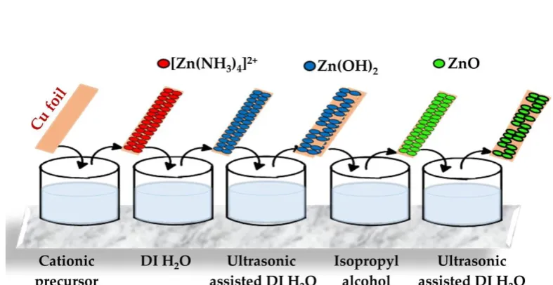
substrates were dipped into ultrasonic-assisted DI water (see Figure 1). Likewise, the above steps
were repeated up to 20 times for preparing the sample with IPA at 30, 50 and 65 ℃labeled the
eliminating the sonication step. The most important deposition parameters and processing
conditions are summarized in Table 1.
Table 1. Sampling details for the deposition of ZnO thin films with IPA at different
temperature.
Deposition
temperature (0C)
Glass substrate Copper foil substrate
Sonication Without sonication Sonication Without sonication
30 G1 G4 C1 C4
50 G2 G5 C2 C5
65 G3 G6 C3 C6
Figure 1. Schematic diagram showing the deposition of ZnO thin film on Cu foil using IPA at different temperature.
The overall reactions involved in the ZnO film deposition are given below [5]:
After deposition, the samples were thoroughly rinsed by DI water, and then dried under laboratory
atmosphere and safely stored into the sample boxes for characterization. Some of the samples were
Zn2+ +2OH
-Zn(OH)2(s)
Zn2+ + 4NH4+ + 4OH
-Zn(OH)
2(s)
ZnO(s) + H
2O
cut into equal pieces for subsequent characterizations as well as 1 hour air-annealing at 250 ℃ ;
while one piece of each batch were kept as as-deposited sample for reference.
2.3. Characterization techniques
The structural properties and phase of the deposited thin films were characterized by XRD
(Philips PANalytical X’Pert MRD) with a CuKα (λ = 0.15406 nm) radiation source in θ-2θ coupled
mode and Raman spectroscopy (Horiba HR800) with 488 nm laser excitation (P≤ 5 mW). Surface morphologies of the samples were imaged by scanning electron microscope (SEM) (Philips XL30
EEG SEM).The optical properties were examined by using a double-beam UV-Visible-NIR
spectrophotometer (Shimadzu UV 2600 ISR plus) in the range of 220-1400 nm. Both diffuse
reflection and transmission spectra were taken to eliminate substrate contributions [35] where
necessary.
3. Results and Discussion
3.1. Structural Characterization
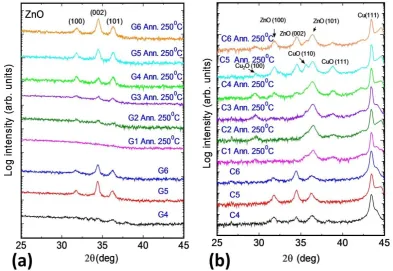
The phase and crystal structure of both as-deposited and annealed samples were examined by
XRD ranging from 2θ = 25-45°and the relating XRD patterns are shown in Figure 2. The deposited samples grown on SLG exhibited three intense peaks at 2θ ≈31.74°, 34.40° and 36.21° which corresponds respectively to (100), (002) and (101) planes of ZnO hexagonal wurtzite structure [35].
No diffraction peaks of Zn(OH)2 are discernible in the XRD patterns (see Figure 2a). In the case of
samples deposited on Cu foil, thin films are preferably deposited along the (101) plane of ZnO,
underlying substrate (see Figure 2b). All of the Cu foil samples produced CuxO/ZnO (x = 1, 2)
structure after post-annealing at 250 ℃ irrespective of the growth temperature with IPA and
sonication process (see top panels in Figure 2). This may be due to the oxidation of Cu foil substrate
as can be seen from both XRD and Raman spectra depicted in Figure 2b and Figure 3b. These
results suggest the formation of Cu-oxide/ZnO heterojunction depend only on the post-annealing
but not on the sonication process and IPA dispersant. Thus, the post-annealing is beneficial for the
formation of CuxO/ZnO heterojunctions [16,45,48]. It is evident from the Figure 2a, the strong
preferential growth along (002) plane of ZnO observed for samples grown on SLG suggesting
highly c-axis oriented films [35] while preferred orientation along (101) plane for samples deposited
on Cu foil [45] as can be seen in Figure 2b. Thus, the crystal growth is strongly influenced by the
substrate types. The strong peak along (002) plane for the as-deposited G5(IPA50) and G6(IPA65)
samples signifies highly oriented c-axis ZnO films [35] which is absent for G4(IPA30) samples,
suggesting that temperature of IPA promotes crystallinity of the as-deposited ZnO film. The
intensity of the concerned diffraction peak is seen to increase further after post-annealing. Therefore,
increasing the IPA temperature and post-annealing improved the crystallinity of the deposited thin
films [35,46]. The same trend is observed for samples deposited on Cu foil. In both cases, without
sonication, samples exhibited better crystallinity as shown in Figure 2 and the good quality films
formed using IPA with a minimum of 50 ℃. Shei et al. [5,46] have reported no film growth below
Figure 2. XRD patterns of both as-made and post-annealed samples grown on (a) SLG and (b) Cu
foil. The diffraction peaks of corresponding materials are shown by arrow sign for clarity.
It is also evident from Figure 2a that highly textured films can be prepared for samples G5(IPA50)
and G6(IPA65) without sonication steps. This may be due to the fact that IPA acts as a better
dispersant compared to ethylene glycol, propylene glycol and DI water reported in refs. [5,46,47]
and results in depositing better quality ZnO thin films.
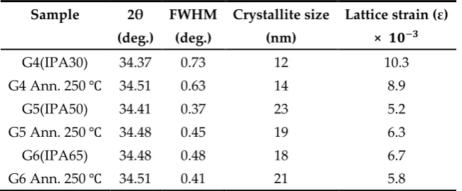
The important structural parameters and mean crystallite sizes (D) of SLG-samples were calculated
by using Scherrer equation [49] to the 002 diffraction peak of ZnO and summarized in Table 2:
D = 𝑘𝜆
𝛽𝑐𝑜𝑠𝜃 (1)
Where, λ= Wavelength of X-ray (0.15406 nm for CuKα radiation source), k= constant which is 0.94,
Table 2. Mean crystallite size and lattice strain of as-made and annealed samples
deposited on SLG using IPA at different temperatures.
Sample 2θ
(deg.)
FWHM
(deg.)
Crystallite size
(nm)
Lattice strain (ε)
× 𝟏𝟎−𝟑
G4(IPA30) 34.37 0.73 12 10.3
G4 Ann. 250 ℃ 34.51 0.63 14 8.9
G5(IPA50) 34.41 0.37 23 5.2
G5 Ann. 250 ℃ 34.48 0.45 19 6.3
G6(IPA65) 34.48 0.48 18 6.7
G6 Ann. 250 ℃ 34.51 0.41 21 5.8
It is evident from the Table 2 that the mean crystallite sizes were 12-23 nm and 18-21 nm
respectively for as-deposited and annealed samples grown on SLG. The crystallite size shows an
increasing trend and the lattice strain decreases with post-annealing at 250 ℃ (G4 Ann. 250 ℃ and
G6 Ann.250 ℃) which signifies the improvement of the crystallinity [5] of the films as can be seen
from Figure 2a. The sample deposited on SLG at 50 ℃ (G5) in the absence of sonication exhibited
the highest crystallinity (D = 23 nm) and minimum lattice strain among all samples with (002)
preferential growth. Therefore, these observations indicated the optimum temperature in presence
of IPA should be 50 ℃ for growing better quality c-axis oriented ZnO thin films without sonication
steps.
3.2. Raman Analysis
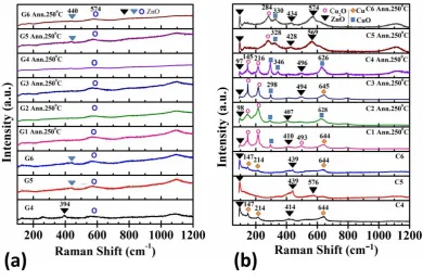
Room temperature Raman measurements of samples deposited on both SLG and Cu foil were
carried out to identify the phase purity of Zn- and Cu-oxides as well as to investigate the effect of
processing conditions on their crystalline structure. Raman spectroscopy is an effective tool
the molecule, crystal structure, chemical bond, etc. [50]. The Raman spectra of the samples deposited
on both SLG and Cu foil are shown in Figure 3a and Figure 3b respectively.
Figure 3. Raman spectra of the samples grown on (a) SLG and (b) Cu foil. The reference Raman shift
values areindicated by different symbols in the figure.
It is clear from Figure 3a that the post-annealing exhibited a broad Raman signal approximately at
574 cm-1 which could be attributed to ZnO [51] for samples G1 Ann 250 ℃ and G2 Ann.250 ℃ for
which XRD peaks were not clear in Figure 2a. In contrast, the samples G5(IPA50) and G6(IPA65)
(without sonication) showed two distinguishable peaks centering at ~440 and ~574 cm-1 which have
been attributed to highly crystalline c-axis oriented ZnO films due to a decrease of defects in the
interior of the crystal [51].
In Figure 3b, the films on Cu foil show Raman peaks centering at 97, 98, 405, 407, 410, 428, 434, 494,
496, 569 and 574 cm-1 correspond to ZnO phase. Moreover, the Raman signals for copper oxide
250 ℃). In addition, peaks at around 147, 214, 644cm-1appeared for samples grown on the Cu foil.
The new Raman shift appeared close to 145, 216, 284, 493 cm-1confirmed the existence of Cu2O
phase while those close to 298, 330, 346, 626 cm-1 are attributed to CuO phase [50-59]. These
observations are indicating the possibility of the facile CuxO/ZnO formation by post-annealing at
temperature as low as 250 ℃. These results are also in consistent with the observed XRD pattern
shown in Figure 2b. From both XRD and Raman analyses, it can be concluded that for depositing
phase pure highly crystalline c-axis oriented ZnO films, it may be better to deposit on SLG and
post-annealing at 250 ℃ for 1 hour results the formation of Cu-oxide/ZnO heterojunction for films
grown on Cu foil.
3.3. Morphological characterization
Figure 4 compares the surface morphologies of thin films grown on both SLG and Cu foil.
From Figure 4a and 4d, it is clearly seen that the samples deposited using IPA at 30 ℃ exhibits
cotton-like amorphous morphology (see also XRD patterns in figure 2). In contrast, compact and
uniformly distributed spherical grains were observed both for IPA50 and IPA65 as-deposited
samples. Thus, at relatively high temperatures good quality films are produced as it provides
sufficient energy for complete conversion of Zn(OH)2 to ZnO [5]. The grain sizes of the films grown
on SLG were larger (~260-300 nm) compared to those grown on Cu foil (~200-230 nm) further
indicating better quality films which supports the XRD data. Some overgrown clusters for Cu
foil-samples can be seen which might be detrimental for device applications. Thus, the film growth
quality is not only affected by the temperature of the IPA but also the types of substrate. Previous
studies reported that relatively higher temperature ( ≥ 95 ℃ ) was required to decrease
isopropyl alcohol is a monohydric alcohol, it forms only inter-molecular hydrogen bond [60] and
affects the deposition process free from releasing thermal energy due to the breaking of
intra-molecular H-bonding. Consequently,Zn(OH)2 species are easily removed through H-bonding
which are loosely adsorbed on the ZnO surface. This property makes IPA to act as a better
dsipersant than ethylene glycol and propylene glycol at relatively low temperatures [61]. The IPA50
sample grown without sonication exhibited a compact microstructural morphology together with
appreciable crystallite size (D = 23 nm) and optical band gap (Eg = 3.37 eV). These observations
assert that the surface morphologies can be controlled by controlling the IPA temperature and by
selecting a suitable substrate.
f
e
d
Figure 4. SEM micrographs of the samples deposited using IPA dispersant at various
temperatures on SLG (a) G4(30 ℃), (b) G5(50 ℃),, (c) G6(65 ℃),; and on Cu foil (d) C4(30 ℃),, (e) C5(50 ℃),, (f) C6(65 ℃),
3.4. Optical characterization
To elucidate the optical characteristics of the as-grown and annealed samples on SLG, both
transmission and diffuse reflection spectra were taken for eliminating underlying substrate
contribution [35]. In case of the samples deposited on Cu foil, only the reflection spectra were
recorded. The diffuse reflection spectra of samples grown without the sonication process at
different temperatures with IPA have been included in Figure 5.
Figure 5. Diffuse reflection spectra of the samples deposited on (a) SLG (b) Cu foil. Both
as-deposited and annealed samples have been included in the same graph. The corresponding
transmission spectra of samples grown on SLG also inserted into Figure 5a for comparisonpurposes.
The vertical lines in Figure 5b indicating the approximate absorption edge of ZnO, Cu2O and CuO.
From Figure 5a it is clearly seen that the samples grown on SLG shows 10-20% reflection in the
wavelength, λ ≈ 380 nm can be seen from both transmission and reflection data which corresponds to ZnO thin films [35]. Samples grown with IPA at higher temperatures (50 and 65 ℃) exhibit
enhanced transparency which further confirmed the better crystallinity and film growth with fewer
defects in the interior crystal [5] and supports the XRD data. In contrast, for the samples grown on
Cu foil (Figure 5b); sharp absorption edges near λ ≈380, 580 and 780 nm can be clearly seen (see fade verticle lines) which could be attribute to ZnO, Cu2O and CuO phase respectively [41,50,62].
The presence of mixed (Cu2O + CuO) phases formed on Cu foil were also confirmed from the XRD
and Raman spectra shown in Figure 2b and Figure 3b.
The optical bandgap was estimated from the Tauc plot generated by using the reflection data and
the Kubelka-Munk function (F(𝑅∞) [35] represented by equation:
(hυF(𝑅∞))𝑛 = A(hυ - 𝐸𝑔) (2)
Where, 𝐸𝑔= Bandgap energy, R∞= Diffuse reflection, h = Planck’s constant and υ = Frequency of the
incident light. ZnO is a direct bandgap material (n=2) which showed direct forbidden transition at
wavelength λ ≈380 nm. Therefore, putting n = 2 in the above equation, the 𝐸𝑔 values obtained by plotting (hυF(𝑅∞))2 vs hυ, where the quantity (hυF(𝑅∞))2 extrapolated to zero [35,41]. The bandgap plots are shown in Figure 6 and 𝐸𝑔 values together with XRD and Raman data are listed
Figure 6. Tauc plots of the samples grown on (a) SLG (b) Cu foil using diffuse reflection data. The
Eg values are calculated by extrapolating the quantity (hυF(R∞))2= 0
Table 3. Optical Bandgap energy and phase identification evidenced from XRD and Raman spectra
for as-made and annealed samples deposited at different temperature using IPA
*Crystallite sizes of the samples grown on SLG substrate are shown in Table 2
From Table 3, it is clear that the Eg values are in the range of 3.37-3.47 eV for as-made samples and
2.98-3.28 eV those for post-annealing samples which could be attributed to the ZnO. However,
post-annealing treatment in case of Cu foil samples exhibited additional Eg in the range of 1.65 –
2.00 eV(see dotted line in Figure 6b) which could be attributed to the CuxO phase[50]. Notice that
samples deposited on SLG exhibited a reduction in bandgap with increasing IPA temperatures due
to improve crystallinity of the ZnO and corroborates the calculated crystallite sizes given in Table 2. Glass Samples Band gap,
Eg(eV) ± 0.01
Cu foil samples Bandgap,
Eg(eV) ± 0.01
Phase composition
(XRD and Raman)
G4(IPA30) 3.48 C4(IPA30) 3.47 ZnO
G5(IPA50) 3.37 C5(IPA50) 3.43 ZnO
G6(IPA65) 3.40 C6(IPA65) 3.45 ZnO
G4 Ann. 250 ℃ 3.28 C4 Ann. 250 ℃ 1.65 & 3.21 CuxO/ZnO
G5 Ann. 250 ℃ 3.21 C5 Ann. 250 ℃ 1.65 & 2.98 CuxO/ZnO
However, post-annealing treatment induced a significant reduction of Eg from roughly 3.4 eV to 3.2
eV is due to the improvement of crystallinity [5] with decline of lattice strain (see Table 2).These
observations imply that post-annealing treatment at 250 ℃ affected deposited films largely
compared to IPA temperatures. It is worth noting that samples grown on Cu foil indicating the
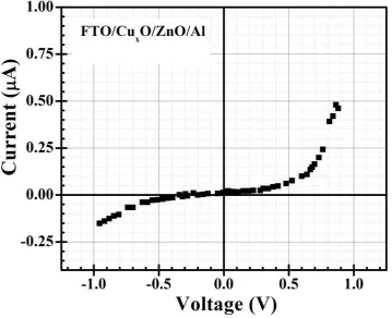
possibility of CuxO/ZnO junction formation by post-annealing (see Table 3). As a proof-of-concept,
I-V characteristics curve of a preliminarily fabricated heterojunction by SILAR method with
FTO/CuxO/ZnO/Al structure is shown in Figure 7, where the diode-like I-V curve confirms that
CuxO/ZnO is successfully formed. However, further experimental investigations are in progress to
assess photovoltaic performance of SILAR grown CuxO/ZnO junctions.
Figure 7. I-V characteristic curve of a SILAR grown heterojunction showing diode-like behaviour
4. Conclusion
ZnO thin films have been synthesized on both SLG and Cu foil and the effect of substrate,
sonication process, and post-annealing on the properties of the deposited films were systematically
investigated. XRD analysis revealed the growth of highly crystalline c-axis oriented ZnO thin films
deposited on SLG with (002) preferred orientation while (101) preferential growth on Cu foil. XRD
and Raman spectroscopy confirmed all of the post-annealing samples produce CuxO/ZnO
heterojunctions irrespective to the growth temperature using IPA and sonication process. Samples
excluding sonication steps exhibited compact and uniformly distributed grain surface
morphologies in the presence of IPA at 50 and 65 ℃ observed from SEM micrographs. The
estimated Eg values were 3.47-3.37 eV for as-made samples and bandgaps were found to be
decreased significantly with increasing annealing temperature due to crystallinity improvement of
the ZnO thin films. The sample grown at 50 ℃ revealed the best quality film grown in this work
with the Eg value of 3.37 eV. This studies proposed that for highly c-axis oriented ZnO thin films, it
may be better to deposit the films on SLG in presence of IPA as a dispersing agent. We hope that
this study will open up a new approach for growing ZnO thin film with less processing steps as
well as solution processable Cu-oxide/ZnO heterojunctions for diverse applications.
Author Contributions:
B.C. Ghos performed the sample synthesis, data analysis and wrote themanuscript. N.I. Tanvir helped with the experimental methodology and characterization setups.
M.A Majed Patwary and M.A. Rahman contributed to the conceptualization, and supervision. S.
results. S.F.U. Farhad conceived the project idea, conceptualization, and led the overall research
works. All authors contributed to the writing, reviewing and editing of the final manuscript.
Acknowledgments:
S.F.U. Farhad and N.I. Tanvir acknowledge the experimental support of the
Energy Conversion and Storage Research Section, Industrial Physics Division, BCSIR Laboratories,
Dhaka 1205, under the scope of R&D project#100-FY2017-2020. M.A.M. Patwary acknowledges the
characterization support of Department of Electrical and Electronic Engineering, Saga University,
Japan. All other authors gratefully acknowledge the logistic support of Physical Chemistry Research
Laboratory, Department of Chemistry, Comilla University, Cumilla 3506, Bangladesh.
Conflicts of Interest: The authors declare no conflicts of interest.
References:
1. Akhtar, M.S.; Riaz, S.; Noor, R.; Naseem, S. Optical and Structural Properties of ZnO Thin
Films for Solar Cell Applications. Adv. Sci. Letters2013, 19(3), 834-841. DOI:
10.1166/asl.2013.4822
2. Muchuweni, E.; Sathiaraj, T.S.; Nyakotyo, H. Physical properties of gallium and aluminium
co-doped zinc oxide thin films deposited at different radio frequency magnetron sputtering
power. Ceram. Int.2016,42, 17706–17710. DOI: http://dx.doi.org/10.1016/j.ceramint.2016.08.091 3. Hsin-Chun, L.; Jia-Chiuan, J.; Chun-Lung, C. Influence of RF magnetron sputtering conditions
Surface & Coatings Tech.2013, 231, 539–542. DOI: http://dx.doi.org/10.1016/j.surfcoat.2012.10.029 4. Ashfold, M.N.R.; Doherty, R.P.; Ndifor-Angwafor, N.G.; Riley, D.J.; Sun, Y. The kinetics of the
hydrothermal growth of ZnO nanostructures. Thin Solid Films 2007, 515(24), 8679-8683.
DOI:10.1016/j.tsf.2007.03.122
5. Shei, S.C.; Lee, P.Y. Influence of rinsing temperature on properties of ZnO thin films prepared
by SILAR method with propylene glycol. J. Alloys Compd. 2013, 546, 165–170. DOI: http://dx.doi.org/10.1016/j.jallcom.2012.07.149
6. Joshi, K.; Rawat, M.; Gautam, S.K.; Singh, R.; Ramola, R.; Mahajan, A. Band gap widening and
narrowing in Cu-doped ZnO thin films. J. Alloy. Compd. 2016, 680, 252–258. DOI: 10.1016/j.jallcom.2016.04.093
7. Rong, P.; Ren, S.; Yu, Q. Fabrications and Applications of ZnO Nanomaterials in Flexible
Functional Devices-A Review. Crit. Rev. Anal. Chem.2018, 49, 336–349. DOI: 10.1080/10408347.2018.1531691
8. Aoun, Y.; Benhaoua, B.; Benramache, S.; Gasmi, B. Effect of deposition rate on the structural,
optical and electrical properties of Zinc oxide (ZnO) thin films prepared by spray pyrolysis
technique. Optik. 2015, 126, 2481–2484. DOI: https://doi.org/10.1016/j.ijleo.2015.06.025
9. Gil, B.; Kavokin, A.V. Giant exciton-light coupling in ZnO quantum dots. Appl. Phys. Lett.
2002, 81, 748–750. DOI: 10.1063/1.1494864
10. Bretagnon, T.; Lefebvre, P.; Valvin, P.; Gil, B.; Morhain, C.; Tang, X. Time resolved
11. Xiong, C.; Yao, R.H.; Wan, W.J.; Xu, J.X. Fabrication and electrical characterization of ZnO rod
arrays/CuSCN heterojunctions. Optik.2014, 125, 785–788. DOI: https://doi.org/10.1016/j.ijleo.2013.07.080
12. Hassan, M.A.M.; Saleh, A.F.; Mezher, S.J. Energy band diagram of In:ZnO/p-Si structures
deposited using chemical spray pyrolysis technique. Appl. Nanosci. 2014, 4, 695–701. DOI:
10.1007/s13204-013-0246-5
13. Manoharan, C.; Pavithra, G.; Bououdina, M.; Dhanapandian, S.; Dhamodharan, P.
Characterization and study of antibacterial activity of spray pyrolysed ZnO: Al thin films.
Appl. Nanosci.2016, 6, 815–825. DOI: 10.1007/s13204-015-0493-8
14. Balaji, G.; Sivakami, R.; Sridharan, M.; Jeyadheepan, K. Preparation and characterization of
refractory ZnO buffer layers for thin film solar cell applications. Mater. Today Proc. 2016, 3,
1730–1736. DOI: https://doi.org/10.1016/j.matpr.2016.04.067 15.
16.
Aoun, Y.; Benhaoua, B.; Benramache, S.; Gasmi, B. Effect of annealing temperature on
structural, optical and electrical properties of zinc oxide (ZnO) thin films deposited by spray
pyrolysis technique. Optik.2015, 126, 5407–5411. DOI: https://doi.org/10.1016/j.ijleo.2015.08.267 Islam, M.R.; Podder, J.; Farhad, S.F.U.; Saha, D.K. Effect of Annealing on the Structural and
Optical Properties of Nano Fiber ZnO Films Deposited by Spray Pyrolysis. Sensors &
Transducers.2011, 134(11), 170-176.
17. Dhanakodi, K.; Thirunavukkarasu, P.; Mariappan, R.; Rajamanickam, A.T. Effect of substrate
https://doi.org/10.1016/j.ijleo.2015.10.143
18. Kenanakis, G.; Katsarakis, N.; Koudoumas, E. Influence of precursor type, deposition time and
doping concentration on the morphological, electrical and optical properties of ZnO and ZnO:
Al thin films grown by ultrasonic spray pyrolysis. Thin Solid Films. 2014, 555, 62–67. DOI: https://doi.org/10.1016/j.tsf.2013.10.015
19. Zhang. Z.; Liao, Q.; Yu, Y.; Wang, X.; Zhang, Y. Enhanced photoresponse of ZnO
nanorods-based self-powered photodetector by piezotronic interface engineering, Nano
Energy.2014, 9, 237-244. DOI: https://doi.org/10.1016/j.nanoen.2014.07.019
20. Roy, S.; Banerjee, N.; Sarkar, C. K.; Bhattacharyya, P. Development of an Ethanol Sensor Based
on CBD Grown ZnO Nanorods. Solid-State Electron. 2013, 87, 43-50. DOI:
https://doi.org/10.1016/j.sse.2013.05.003
21. Singh, O.; Kohli, N.; Singh, R.C. Precursor Controlled Morphology of Zinc Oxide and its
Sensing Behavior. Sens. Actuators B. 2013, 178, 149-154. DOI:
https://doi.org/10.1016/j.snb.2012.12.053
22. Schmidt-Mende, L.; MacManus-Driscoll, J.L. ZnO–nanostructures, defects and devices.
Materials Today.2007, 10(5), 40-48. DOI: https://doi.org/10.1016/S1369-7021(07)70078-0
23. Kadota, M. Surface Acoustic Wave Characteristics of a ZnO/Quartz Substrate Structure
Having a Large Electromechanical Coupling Factor and a Small Temperature Coefficient. Jpn.
J. Appl. Phys. 1997, 36, 3076-3080. DOI: https://doi.org/10.1143/JJAP.36.3076
24. Ennaceri, H.; Erfurt, D.; Wang, L.; Köhler, T.; Taleb, A.; Khaldoun, A.; El Kenz, A.; Benyoussef,
coatings for CSP application. Surf. Coatings Technol. 2016, 298, 103–113. DOI: https://doi.org/10.1016/j.surfcoat.2016.04.048
25. Wang, Z.L.; Song, J. Piezoelectric Nanogenerators Based on Zinc Oxide Nanowire Arrays.
Science. 2006,312, 242-246. DOI: 10.1126/science.1124005
26. Lee, P.Y.; Chang, S.P.; Chang, J.F.; Hsu, E.N.; Chang, S.J. Highly Transparent Nanostructured
Zinc Oxide Photodetector Prepared by Successive Ionic Layer Adsorption and Reaction. Int. J.
Electrochem. Sci.2013, 8, 6425-6432.
27. Gao, X.; Xiaomin, L.; Weidong, Y. Preparation and characterization of highly oriented ZnO
film by ultrasonic assisted SILAR method. J. Wuhan Uni. Tech. Mater. Sci. Ed. 2005, 20, 23-26.
DOI: https://doi.org/10.1007/BF02835019
28. Ajuba, A.E.; Ezugwu, S.C.; Ezekoye, B.A.; Ezema, F.I.; Asogwa, P.U. Influence of pH on the
structural, optical and solid state properties of chemical bath deposited ZnO thin films. J.
Optoelec. Biomed. Mater. 2010, 2(2), 73-78.
29. Villanueva, Y.Y.; Liu, D.R.; Cheng, P.T. Pulsed laser deposition of zinc oxide. Thin Solid Films
2006, 501, 366-369. DOI: https://doi.org/10.1016/j.tsf.2005.07.152
30. Cruz, M.R.A.; Ceballos-Sanchez, O.; Luevano-Hipolito, E.; Torres-Martı´nez, L.M. ZnO thin
films deposited by RF magnetron sputtering: Effects of the annealing and atmosphere
conditions on the photocatalytic hydrogen production. Int. J. Hydro. Energ. 2018, 43(22),
10301-10310. DOI: https://doi.org/10.1016/j.ijhydene.2018.04.054
31. Ye, J.; Gu, S.; Zhu, S.; Chen, T.; Hu, L.; Qin, F.; Zhang, R.; Shi, Y.; Zheng, Y. The growth and
151-156. DOI: https://doi.org/10.1016/S0022-0248(02)01474-4
32. Islam, M.R.; Rahman, M.; Farhad, S.F.U.; Podder, J. Structural,optical and photocatalysis
properties of sol-gel deposited Al-doped ZnO thin films. Surfaces and Interfaces. 2019, 16,
120-126. DOI: https://doi.org/10.1016/j.surfin.2019.05.007
33. Baruah, S.; Dutta, J. Effect of seeded substrates on hydrothermally grown ZnO nanorods. J.
Sol-Gel Sci. Tech.2009, 50(3), 456-464. DOI: https://doi.org/10.1007/s10971-009-1917-2
34. Kato, H.; Sano, M.; Miyamoto, K.; Yao, T. High quality ZnO epilayers grown on Zn-face ZnO
substrates by plasma-assisted molecular beam epitaxy. J. Cryst. Growth 2004, 265, 375-381.
DOI: https://doi.org/10.1016/j.jcrysgro.2004.02.021
35. Farhad, S.F.U.; Tanvir, N.I.; Bashar, M.S.; Hossain, M.S.; Sultana, M.; Khatun, N.; Facile
synthesis of oriented zinc oxide seed layer for the hydrothermal growth of zinc oxide
nanorods. Bangladesh J. Sci. Ind. Res. 2018, 53(4), 233-244. DOI: 10.3329/bjsir.v53i4.39186
36. Farhad, S.F.U.; Tanvir, N.I.; Bashar, M.S.; Sultana, M. Synthesis and characterization of c-axis
oriented Zinc Oxide thin films and its use for the subsequent hydrothermal growth of Zinc
Oxide nanorods. MRS Advances. 2019, 4(16), 921-928. DOI:https://doi.org/10.1557/adv.2019.65
37. Zhenghua, S.; Kaiwen, S.; Zili, H.; Fangyang, L.; Yanqing, L.; Jie, L.; Yexiang L. Fabrication of
ternary Cu–Sn–S sulfides by a modified successive ionic layer adsorption and reaction (SILAR) method. J. Mater. Chem.2012, 22, 16346–16352.DOI: https://doi.org/10.1039/C2JM31669B 38. Haridas, D.D.; Surendra, K.S.; Ninad, B.V.; Lohar, G.M.; Vijay, J.F. Synthesis and
characterization of ZnO thin film by low cost modified SILAR technique. AIMS Materials
39. Raidou, E.A.; Benmalek, F.; Sall, T.; Aggour, M.; Qachaou, A.; Laanab, L.; Fahoume, M.
Characterization of ZnO Thin Films Grown by SILAR Method. Open Access Library Journal.
2014, 01(03), 1-9. DOI: 10.4236/oalib.1100588
40. Offiah, S.U.; Agbo, S.N.; Sutta, P.; Maaza, M.; Ugwuoke, P.E.; Osuji, R.U.; Ezema, F.I. Journal of
Solid State Electrochemistry. 2017, 21, 2621–2628. DOI: https://doi.org/10.1007/s10008-017-3514-6 41. Farhad, S.F.U.; Hossain, M.A.; Tanvir, N.I.; Akter, R.; Patwary, M.A.M.; Shahjaha, M.;
Rahman, M.A. Structural, optical, electrical, and photoelectrochemical properties of cuprous
oxide thin films grown by modified SILAR method. J. Mater. Sci. Semicon. Process. 2019, 95,
68-75. DOI: https://doi.org/10.1016/j.mssp.2019.02.014
42. Mageshwari, K.; Sathyamoorthy, R. Physical properties of nanocrystalline CuO thin films
prepared by the SILAR method. Mater. Sci. Semicond. Process. 2013, 16(2), 337–343. DOI: https://doi.org/10.1016/j.mssp.2012.09.016
43. Patil, A.S.; Lohar, G.M.; Fulari, V.J. Structural, morphological, optical and
photo-electrochemical cell properties of copper oxide using modified SILAR method. J. Mater.
Sci. Mater. Electron. 2016, 27(9), 9550–9557. DOI: https://doi.org/10.1007/s10854-016-5007-2 44.
45.
Beaini, S.S.; Kronawitter, C.X.; Carey V.P.; Mao, S.S. ZnO deposition on metal substrates:
Relating fabrication, morphology, and wettability. J. App. Phy.2013, 113, 184905-184914. DOI:
https://doi.org/10.1063/1.4803553
Raidou, A.; Lharch, M.; Nouneh, K.; Aggour, M.; Qachaou, M.; Laanab, L.; Fahoume, M. Effect
Renewable and Sustainable Energy Conference, IRSEC 2014, Ouarzazate, Morocco, 17-19 October
2014. DOI: 10.1109/IRSEC.2014.7059829
46. Shei, S.C.; Lee, P.Y.; Chang, S.J. Effect of temperature on the deposition of ZnO thin films by
successive ionic layer adsorption and reaction. App. Surf. Sci. 2012, 258, 8109-8116. DOI:
http://dx.doi.org/10.1016/j.apsusc.2012.05.004
47. Shei, S.C.; Chang, S.J.; Lee, P.Y. Rinsing Effects on Successive Ionic Layer Adsorption and
Reaction Method for Deposition of ZnO Thin Films. J. Electrochem. Soc. 2011, 158(3), H208-H213.
DOI: 10.1149/1.3528306
48.
49.
50.
51.
Farhad, S.F.U.; Majumder, S.; Hossain, M.A.; Tanvir, N.I.; Akter, R.; Patwary, M.A.M. Effect of
Solution pH and Post-annealing temperatures on the Optical Bandgap of the Copper Oxide
Thin Films Grown by modified SILAR Method. MRS Advances 2019, 4(16), 937-944. DOI:
10.1557/adv.2019.139
Chowdhury, R.I.; Hossen, M.A.; Mustafa, G.; Hussain, S.; Rahman, S.N.; Farhad, S.F.U.;
Murata, K.; Tambo, T.; Islam, A.B.M.O. Characterization of Chemically-deposited Cadmium
Sulfide Thin Films. Int. J. Modern Phys. B.2010, 24, 5901-5911. DOI: 10.1142/S021797210055147
Farhad, S.F.U.; Webster, R.F.; Cherns, D. Electron Microscopy and Diffraction studies of
Pulsed Laser deposited Cuprous oxide thin films grown at low substrate temperature.
Materialia.2018, 3, 230-238. DOI: https://doi.org/10.1016/j.mtla.2018.08.032
Singh, S.; Srinivasa, R.S.; Major, S.S. Effect of substrate temperature on the structure and optical
properties of ZnO thin films deposited by reactive rf magnetron sputtering. Thin Solid Films
52. Patwary, M.A.M.; Saito, K.; Guo,Q.; Tanaka,T. Influence of oxygen flow rate and substrate
positions on properties of Cu-oxide thin films fabricated by radio frequency magnetron
sputtering using pure Cu target. Thin Solid Films. 2019, 675, 59–65. DOI: https://doi.org/10.1016/j.tsf.2019.02.026
53. Koyano, M.; QuocBao, Q.; ThanhBinh, L.T.; HongHa, L.; NgocLong, N.; Katayama, S.I.
Photoluminescence and Raman Spectra of ZnO Thin Films by Charged Liquid Cluster Beam
Technique. Phys. Stat. Sol. 2002, 193, 125–131. DOI: https://doi.org/10.1002/1521-396X(200209)193:1<125::AID-PSSA125>3.0.CO;2-X
54. Yahia, S.B.; Znaidi, L.; Kanaev, A.; Petitet, J. P. Raman study of oriented ZnO thin films
deposited by sol–gel method. Spectrochimica Acta Part A 2008, 71, 1234–1238. DOI:
10.1016/j.saa.2008.03.032
55. Farhad, S.F.U.; Cherns, D.; Smith, J.A.; Fox, N.A.; Fermín, D.J. Pulsed laser deposition of single
phase n- and p-type Cu2O thin films with low resistivity. Materials and Design. 2020, 193,
108848-108855. DOI: https://doi.org/10.1016/j.matdes.2020.108848
56. Patwary, M.A.M.; Ho, C.Y.; Saito, K.; Guo, Q.; Yu, K.M.; Walukiewicz, W.; Tanaka,T.Effect of
oxygen flow rate on properties of Cu4O3 thin films fabricated by radio frequency magnetron
sputtering. J. Appl. Phys.2020, 127, 085302. DOI: https://doi.org/10.1063/1.5144205
57. Pandey, P.; Parra, M.R.; Haque, F.Z. Effects of annealing temperature optimization on the
efficiency of ZnO nanoparticles photoanode based dye sensitized solar cells. J Mater Sci: Matter
58.
59.
60.
61.
Khan, A. Raman Spectroscopic Study of the ZnO Nanostructures. J. Pak. Mater. Soc. 2010, 4(1),
5-9.
Li, H.; Ban, L.; Niu, Z.; Huang, X.; Meng, P.; Han, X.; Zhang. Y.; Zhang, H.; Zhao, Y.
Application of CuxO-FeyOz Nanocatalysts in Ethynylation of Formaldehyde.
Nanomaterials. 2019, 9(9), 1301-1315. DOI: https://doi.org/10.3390/nano9091301
Mauricio Muñoz-Muñoz, Y.; Guevara-Carrion, G.; Jadran, V. Molecular Insight into the Liquid Propan-2-ol + Water Mixture. J. Phys. Chem. B2018, 122(37), 8718–8729. DOI:
https://doi.org/10.1021/acs.jpcb.8b05610
Crupi, V.; Majolino, D.; Migliardo, P.; Venuti, V. Inter- and intramolecular hydrogen bond in
liquid polymers: a Fourier transform infrared response. Molecular Physics, 2000, 98, 1589-1594.
DOI: https://dx.doi.org/10.1080/00268970009483364
62. Daira, R.; Kabir, A.; Boudjema, B.; Sedrati, C. Structural and optical transmittance analysis of
CuO thin films deposited by the spray pyrolysis method. Solid Sate Sci. 2020, 104,