Article
1
Fully solution-processable fabrication of
2
multi-layered circuits on flexible substrate using laser
3
Seok Young Ji1, 2, Wonsuk Choi2, 3, Hoon-Young Kim2, 3, Jin-Woo Jeon3, Sung-Hak Cho2, 3 and Won
4
Seok Chang1, 2,*
5
1 Department of Nano Mechanics, Nanomechanical Systems Research Division, Korea Institute of Machinery
6
and Materials, 156 Gajeongbuk-Ro, Yuseong-Gu, Daejeon 34103, Republic of Korea
7
2 Department of Nano-Mechatronics, Korea University of Science and Technology (UST), 217 Gajeong-Ro,
8
Yuseong-Gu, Daejeon 34113, Republic of Korea
9
3 Department of Laser & Electron Beam Application, KIMM, Korea Institute of Machinery and Material, 156
10
Gajeongbuk-Ro, Yuseong-Gu, Daejeon 34103, Korea
11
* Corresponding Author: [email protected]; Tel.: +82-42-868-7134
12
Abstract: The development of printing technologies has enabled the realization of electric circuit
13
fabrication on flexible substrate. However, the current technique remains restricted to single-layer
14
patterning. In this paper, we demonstrate a fully solution-processable patterning approach for
15
multi-layer circuits using a combined method of laser sintering and ablation. Selective laser
16
sintering of silver (Ag) nanoparticle-based ink is applied to make conductive patterns on a
17
heat-sensitive substrate and insulating layer. The laser beam path and irradiation fluence are
18
controlled to create circuit patterns for flexible electronics. Microvia drilling using femtosecond
19
laser through the polyvinylphenol-film insulating layer by laser ablation, as well as sequential
20
coating of Ag ink and laser sintering, achieves an interlayer interconnection between multi-layer
21
circuits. The dimension of microvia is determined by a sophisticated adjustment of laser focal
22
position and intensity. Based on these methods, the flexible electronic circuit with
23
chip-size-package light-emitting diodes was successfully fabricated and demonstrated with
24
functional operations.
25
Keywords: Interconnection, multi-layer patterning, laser sintering, femtosecond laser ablation
26
27
1. Introduction
28
Functional-ink-based printing technology has greatly advanced in recent years for use with
29
flexible electronics [1,2]. Printing techniques, such as micro-contact (μ-contact) [2–4], inkjet [5–8],
30
screen [9,10], flexography [11,12] and gravure [13–15] approaches, have made it possible to fabricate
31
conductive patterns in large areas at a reasonable cost. As printing technologies have matured,
32
electronic applications, such as resistor–capacitor circuits [16], radio frequency identification [17],
33
sensors [18], displays [19], organic field-effect transistors [20,21], and solar cells [22], have been
34
reported. However, these techniques support only single-layer circuit printing and are thus not well
35
suited for the manufacturing of multi-layer circuits. Multi-layer circuit manufacturing is desirable
36
because it not only reduces the circuit routing complexity, but it also enables fabrication of
37
integrated circuits (IC) [23–26]. Moreover, multi-layer circuit fabrication requires stacking of
38
single-layer circuits and hole creation for interconnecting layer-to-layer. Previous studies suggested
39
an interconnection method by dry etching [23,24], which is slow, expensive, and harmful to the
40
environment. Another approach is to use a drilling mechanism that employs a hole opener [26]. This
41
method consumes a small amount of energy and enables interconnection in a short time.
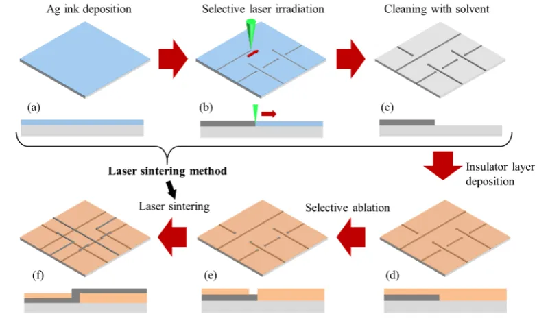
42
Nevertheless, it is only available for the fabrication of double-sided circuits, and it is difficult to
43
implement miniaturization of electronic device because the minimum via-hole size is 500 μm.
44
45
46
In this study, we developed a fully solution-processable fabrication process for the multi-layer
47
circuit on flexible substrate using a combined method of selective laser sintering (SLS) and ablation
48
(SLA). SLS with double irradiation enables low-temperature metal patterning without damaging the
49
heat-sensitive substrate [27]. The double irradiation method uses a higher laser power than the
50
single irradiation method to fabricate electrodes with high conductivity on heat-sensitive substrates.
51
In addition, we introduced femtosecond laser-based SLA through a polyvinylphenol (PVP) insulator
52
to create microvias for interconnections between layers. For ablating insulating layers without
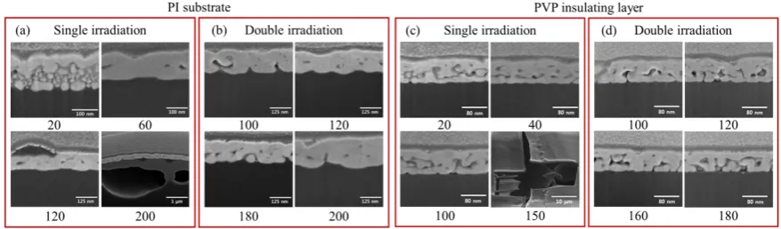
53
damaging the bottom electrode, we investigated the correlation between a femtosecond laser and
54
materials such as sintered Ag electrode and PVP insulating layer. The laser-based process was
55
managed by the optimized conditions of laser fluence and focal position to achieve a suitable
56
microvia diameter and depth. A multi-layered flexible electric circuit was constructed using the
57
suggested process and operated with assembly of chip-size-package light-emitting diodes (LEDs)
58
for process verification.
59
2. Materials and Methods
60
2.1 Experimental setup
61
A continuous wave (CW) laser (mpc6000, Ventus) was implemented for the SLS, which has a
62
maximum power of 1.6 W, power stability of <0.4% rms, and beam size of 1.5 ± 0.1 mm. A galvano
63
scanner (intelliSCAN®10, SCANLAB) was used for the laser beam scanning. It has a maximum
64
making speed of 3.0 m/s, scan area of 45 × 45 mm2, scan angle of ±22 degrees, and nonlinearity of <3.5
65
mrad. The SLA source was the second harmonic 515 nm femtosecond Yb:KGW laser from Light
66
Conversion (Pharos SP), which has a maximum power of 6 W, pulse duration of 190 fs, maximum
67
pulse energy of >1.0 mJ, and beam quality of TEM00; M2 <1.3. The laser beams were focused at a
68
normal incidence onto the insulating layer by a single x50 infinity corrected objective lens with a the
69
numerical aperture (NA) of 0.42.
70
71
2.2 Materials and preparation
72
For this study, commercially available conductive ink and insulating layer were applied. The silver
73
(Ag) nanoparticle (NP) inks were from Harima Chemicals, Inc. (NPS-J) and had Ag particles of a 12
74
nm mean diameter and metal content of 65%. The poly (vinylphenol) (PVP) and methylated poly
75
(melamine-co-formaldehyde) (MMF) for the polymer insulator layer were purchased from
76
Sigma-Aldrich and used without further purification. The PVP-MMF solution (PVP : MMF = 1 : 1.25)
77
was dissolved in propylene glycol monomethyl ether acetate (PGMEA) at a solid concentration of
78
100 mg/ml. These solutions were then filtered through a 0.45 μm polytetrafluoroethylene syringe
79
filter before deposition by spin-coating.
80
81
2.3 Multi-layer patterning process
82
Figure 1 shows a detailed multi-layer patterning process flow. First, the bottom pattern was
83
prepared by SLS on PI substrate, as shown in Figure 1(a–c). The Ag NP ink was spin-coated onto the
84
PI substrate, followed by pre-drying in ambient conditions on a hot plate at 70°C to stop the flow of
85
the Ag NP ink (Figure 1(a)). The thickness of the Ag NP ink films before sintering was ~70 nm. The
86
prepared Ag NP film was selectively sintered by a scanning laser beam with a Galvano scanner to
87
draw the desired patterns (Figure 1(b)). Then, the un-sintered Ag NPs were simply washed away
88
with the solvent (toluene) to reveal the metal patterns (Figure 1(c)).
To remove the remaining impurities and increase the surface energy, the substrates with patterns
90
were sequentially cleaned in an ultrasonic bath with deionized water and 2-propanol for 10 min
91
each. The PVP solution was spin-coated onto the cleaned substrates, followed by pre-baking at 120
92
°C for 10 min and inducing thermal cross-linking at 220 °C for 60 min (Figure 1(d)). The thickness of
93
the PVP polymer insulator films was ~500 nm. Next, the insulator film was selectively ablated using
94
the femtosecond laser (Figure 1(e)). The laser sintering method was sequentially applied to form the
95
top patterns and interconnection between the top and bottom circuit (Figure 1(f)).
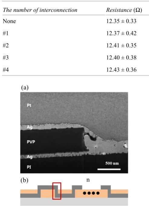
96
97
98
Figure 1. Schematic of the multi-layer patterning process using selective laser sintering and ablation
99
100
3. Results
101
To fabricate the multi-layer circuit, conductive patterns and the interconnection between layers
102
must be achieved on the heat-sensitive substrate without thermal damage. Figure 2 shows
103
cross-sectional scanning electron microscope (SEM) images of patterns using laser sintering at
104
various laser powers using the single irradiation method (Figure 2(a), (c)) and double irradiation
105
method (Figure 2(b), (d)) on the PI substrate and PVP insulating layer. The Ag NPs show a
106
high-energy absorption rate at a wavelength of 532 nm [31], which enables surface sintering
107
features even at a low laser power of 10 mW. The patterns fabricated with a laser power of 40 mW
108
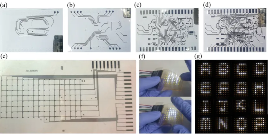
or lower show surface sintering; however, the interior ink of the pattern is not completely sintered.
109
Thus, it was detached or damaged during the cleaning process due to insufficient adhesion of the
110
partially sintered Ag layer with the substrate.
111
A higher laser power should give a higher electric conductivity and adhesion of sintered Ag
112
NP film than lower ones because of the incomplete coalescence of Ag nanoparticles and the
113
diminished electron scattering [28–30]. However, when we induced a high laser power for
114
obtaining high electric conductivity, portions of the patterns incurred defects and burning effects
115
because the higher laser power directly irradiated the heat-sensitive substrate through the Ag NP
116
layer. It thus influenced the pattern conditions, such as conductivity and roughness. To circumvent
117
this problem, we used a double laser sintering method, which involved two processes: first,
118
irradiation using a low laser power was performed on Ag NP films to pre-sinter the surface layer,
called surface-sintering (SS); second, the un-sintered interior ink was post-sintered by the high laser
120
power, called complete-sintering (CS).
121
In the SS step, a low (less than 20 mW) laser power successfully sintered the surface layer,
122
which preserved the heat-sensitive substrate by the following high-power laser irradiation. When
123
we irradiated with the high-power laser in the CS step, the interior Ag NP layer of the pattern was
124
sintered by vertical heat conduction. The substrates remained unaffected by the direct laser
125
irradiation on account of the surface layer sintered in the previous SS step.
126
Figure 2(b) shows optical images of the patterns using the double irradiation method. For this
127
method, we employed 20 mW of laser power in the SS step and varied the laser power in the CS
128
step. It was confirmed that the pattern was fabricated without damage in the conditions with the
129
high laser-power, which usually caused defects in the single irradiation method as shown in Figure
130
2(a), (c). Nevertheless, some patterns incurred defects owing to the excessive vertical heat
131
conduction, which affected the substrate in the CS step (laser power of 250 mW and 200 mW on the
132
PI substrate and PVP insulating layer, respectively (Figure S1(b) and S2(b)).
133
134
135
Figure 2. Cross-sectional SEM images of Ag electrode sintered by (a), (c) single and (b), (d) double
136
laser irradiation with different power on PI substrate and PVP insulating layer. The numbers
137
underneath the SEM image indicate laser power.
138
139
To verify the patterns condition when irradiating with various laser powers, we measured the
140
conductivity for the three process conditions: single laser irradiation, double irradiation with
141
pre-sintering at a laser power of 10, and the latter approach at a laser power of 20 mW. The laser
142
power was adjusted from 60 mW to 250 mW because the pattern fabricated with less than 40 mW
143
was partially detached during the cleaning process. We attempted an experiment on PI substrate
144
(Figure S3(a)) and PVP insulating layer (Figure S3(b)), respectively. The graphs of laser-power
145
versus conductivity show that the measured conductivity increased as the laser power increased.
146
The trend of increasing conductivity with laser power is readily elucidated by various sintering
147
models [31-34]. It is noted that the Ag NP grain-growth mechanisms upon laser irradiation [31] can
148
explain the high conductivity at a high laser-power; nonetheless, thermal damage was incurred by
149
the printed pattern. The fabricated pattern with SS at 20 mW and CS at 240 mW had the highest
150
conductivity, but it has been confirmed that substrate is damaged by 50 % probability. We selected
151
a laser power that did not damage on the substrate even after 100 repetition test.
152
Consequentially, we fabricated the pattern with a conductivity of 6.21 × 10⁵ S/cm and an rms
153
roughness of 7.09 ± 0.5 nm on PI without damage using the double irradiation method with SS at a
154
laser power of 20 mW and CS at 160 mW. This result was approximate to the conductivity of bulk
155
silver of 6.3 × 10⁵ S/cm. On the other hand, the pattern on the PVP layer had slightly lower
156
conductivity of 4.25 × 10⁵ S/cm. It is because we induced relatively low laser power of 20 mW and
157
140 mW for SS and CS, respectively, considering the PVP layer thickness of 500 nm.
158
The multi-layer circuit manufacturing includes not only fabrication of conductive patterns on a
159
heat-sensitive substrate, but also an interconnection between layers. Thus, selective laser ablation
160
using femtosecond laser was performed to make microscale via-hole (named “microvia”) through
161
the insulating PVP layer without damaging the bottom electrode. We need to know the ablation
threshold of sintered Ag electrode (EAg) and PVP insulating layer (EPVP) for ablating of PVP layers in
163
interconnection region without damage on bottom Ag electrode. The laser fluence would be
164
determined between EPVP and EAg. To determine the ablation thresholds of each material for the
165
complete series of ablation spot, the relevant ablation areas have to be plotted versus laser pulse
166
fluence on a logarithmic scale. Then the ablation threshold of each material can be derived by
167
extrapolating the relationship between laser fluence and the relevant areas on a Liu-plot [31,32]. For
168
this purpose, the objective lens was focused on the surface of the materials, and the relevant
169
ablation area was observed and measured with an optical microscope (OM), while increasing or
170
decreasing laser fluence. The results of this analysis are shown in Figure 3. It is obvious that the
171
value of EPVP (0.701 J/cm2) for ablating the insulating layer is about a half of EAg (1.402 J/cm2). Based
172
on the results, we can fabricate microvia that can be used for interconnection by selected laser
173
fluence (~0.9 J/cm2). The microvia diameter ranged from 100 to 10 μm, and the stable minimum
174
diameter was 10 μm. After fabricating the microvia, the Ag NP ink filled the empty microvia space
175
during the spin-coating step of the SLS process. In the laser-sintering step of the top pattern, the
176
laser beam path was specifically modified for the double CS step on the microvia position to
177
increase the heat penetration depth.
178
179
180
Figure 3. Liu-plot of ablation areas for laser irradiation on sintered Ag electrode and PVP insulating
181
layer. The value of ablation threshold has been extracted from experimental results. (Liu-plot
182
non-linear fitting).
183
184
Figure 4(a) shows a cross-sectional scanning electron microscopy (SEM) image of the
185
interconnected part between the top and bottom layers. To confirm that the interconnection had
186
consistency on patterns, we measured the resistance of the patterns with a different number of
187
interconnections, as shown in Figure 4(b). Table 1 shows that the resistance has similar values
188
regardless of the number of interconnections. Thus, we could expect that the electric current flow
189
was not affected by the interconnection. Using the multi-layer patterning process with
190
interconnections, more complicated circuits with two or more layers could be fabricated.
Table 1. The Measured resistances (mean ± standard deviation) according to the number of
200
interconnections.
201
The number of interconnection Resistance (Ω)
None 12.35 ± 0.33
#1 12.37 ± 0.42
#2 12.41 ± 0.35
#3 12.40 ± 0.38
#4 12.43 ± 0.36
202
203
Figure 4. (a) Cross-sectional SEM image of the interconnected region between top and bottom Ag
204
electrode. (b) Schematic of cross-sectional sample structure fabricated by SLS and SLA.
205
206
We designed a flexible micro-controller-unit (MCU) circuit with triple layers consisting of a
207
ground circuit on the first layer, a voltage circuit on the second layer, and a main circuit on the third
208
layer. The device circuit has full size of 25 × 45 mm2 with a line width of 30 μm,. Figures 5 (a–c)
209
show the separated patterns of the ground, voltage, and main circuit on the PI, respectively. To
210
achieve a multi-layered circuit on the same substrate, it usually requires a complex etching and
211
deposition process for connecting between layers. We demonstrated that the entire MCU circuit
212
could be fabricated by the multi-layer patterning process on the PI as shown in Figure 5(d).
213
Finally, we try to manufacture a functional device using the multi-layer patterning process to
214
verify that this process is applicable to flexible applications. As shown in Figure 5(e), the 8 × 16 dot
215
matrix circuit was obtained with a full device size of 45 × 85 mm2, and LED connection pad of 150 ×
216
80 μm2. After patterning the dot matrix circuits, the chip-size-package LEDs were mounted on the
217
prepared circuit. An MCU (Texas Instruments, mpc430), connected using copper wires (diameter
218
~500 μm), was used to input the signal to the LEDs. As shown in Figure 5(f), the LED operation
219
according to the input signal was well maintained during the bending state, thus demonstrating
220
excellent possibilities for flexible electronic device applications. Figure 5(g) shows the various
221
capital letters (from A to P) represented by the controlled input pins on the dot matrix.
223
Figure 5. Optical photographs of MCU board circuit for (a) ground (first layer), (b) voltage (second
224
layer), (c) main (third layer), and (d) final circuits fabricated by the multi-layer patterning process
225
on the PI substrate. (e) Fabricated dot-matrix circuit using the multi-layer patterning process. (f)
226
Bending test of the fabricated electric device. (g) Expression of various capital letters using LED.
227
5. Conclusions
228
Using a combined SLS and SLA method, we developed a fully solution-processable fabrication
229
process for multi-layer patterns on flexible substrate. We verified that the electric resistance of the
230
fabricated patterns was not affected by the number of interconnections. Moreover, to demonstrate
231
that the multi-layer patterning process can be used for flexible applications an electric device circuit
232
with two and three layers was fabricated using this process.
233
This research provides several guidelines for the study of the laser sintering method on
234
heat-sensitive substrate and the fabrication of multi-layer patterns. In addition, it enables the
235
achievement of a desirable microvia diameter and suitable depth by controlling the laser focus
236
position and intensity to make interconnections. The electric device fabricated with our technology
237
showed successful operation. We expect that the proposed approach can be a key technology for
238
implementing user-designed flexible electronic devices in near future.
239
240
Acknowledgments: This work was supported by the Center for Advanced Soft-Electronics funded by the
241
Ministry of Science, ICT and Future Planning (CASE-2016M3A6A5929198) Korea, and the Basic Research Fund
242
of Korea Institute of Machinery & Materials (SC1240).
References
245
1. Gupta, R.; Walia, S.; Hösel, M.; Jensen, J.; Angmo, D.; Krebs, F. C.; Kulkarni, G. U. Solution processed large
246
area fabrication of Ag patterns as electrodes for flexible heaters, electrochromics and organic solar cells. J.
247
Mater. Chem. A2014, 2, 10930.
248
2. Ko, S. H.; Pan, H.; Grigoropoulos, C. P.; Fréchet, J. M. J.; Luscombe, C. K.; Poulikakos, D. Lithography-free
249
high-resolution organic transistor arrays on polymer substrate by low energy selective laser ablation of
250
inkjet-printed nanoparticle film. Appl. Phys. A Mater. Sci. Process.2008, 92, 579–587.
251
3. Loo, Y.; Someya, T.; Baldwin, K. W.; Bao, Z.; Ho, P.; Dodabalapur, A.; Katz, H. E.; Rogers, J. A. Soft,
252
conformable electrical contacts for organic semiconductors: high-resolution plastic circuits by lamination.
253
Proc. Natl. Acad. Sci. U. S. A.2002, 99, 10252–6.
254
4. Zaumseil, J.; Someya, T.; Bao, Z.; Loo, Y. L.; Cirelli, R.; Rogers, J. A. Nanoscale organic transistors that use
255
source/drain electrodes supported by high resolution rubber stamps. Appl. Phys. Lett.2003, 82, 793–795.
256
5. Chung, S.; Jang, M.; Ji, S. B.; Im, H.; Seong, N.; Ha, J.; Kwon, S. K.; Kim, Y. H.; Yang, H.; Hong, Y. Flexible
257
high-performance all-inkjet-printed inverters: Organo-compatible and stable interface engineering. Adv.
258
Mater.2013, 25, 4773–4777.
259
6. Chen, S.; Su, M.; Zhang, C.; Gao, M.; Bao, B.; Yang, Q.; Su, B.; Song, Y. Fabrication of Nanoscale Circuits on
260
Inkjet-Printing Patterned Substrates. Adv. Mater.2015, 27, 3928–3933.
261
7. Yu, P.-C.; Hong, C.-C.; Liou, T.-M. Bendable transparent conductive meshes based on multi-layer
262
inkjet-printed silver patterns. J. Micromechanics Microengineering2016, 26, 35012.
263
8. Jeong, J. A.; Kim, J.; Kim, H. K. Ag grid/ITO hybrid transparent electrodes prepared by inkjet printing. Sol.
264
Energy Mater. Sol. Cells2011, 95, 1974–1978.
265
9. Bao, Z. N.; Feng, Y.; Dodabalapur, A.; Raju, V. R.; Lovinger, A. J. High-performance plastic transistors
266
fabricated by printing techniques. Chem. Mater.1997, 9, 1299.
267
10. Garnier, F.; Hajlaoui, R.; Yassar, A.; Srivastava, P. All-Polymer Field-Effect Transistor Realized by Printing
268
Techniques. Science (80-. ).1994, 265, 1684–1686.
269
11. Leppäniemi, J.; Huttunen, O. H.; Majumdar, H.; Alastalo, A. Flexography-Printed In2O3 Semiconductor
270
Layers for High-Mobility Thin-Film Transistors on Flexible Plastic Substrate. Adv. Mater.2015, 27,
271
7168–7175.
272
12. Furukawa, T.; Kawamura, N.; Inoue, J.; Nakada, H.; Koden, M. OLED Lighting Devices Fabricated by
273
Flexography Printing of Silver Nanowire and Conducting Polymer Tadahiro Furukawa *, Norifumi
274
Kawamura *, Junichi Inoue **, Hitoshi Nakada *, and Mitsuhiro Koden *. 2015, 1355–1358.
275
13. Koo, H.; Lee, W.; Choi, Y.; Sun, J.; Bak, J.; Noh, J.; Subramanian, V.; Azuma, Y.; Majima, Y.; Cho, G.
276
Scalability of carbon-nanotube-based thin film transistors for flexible electronic devices manufactured
277
using an all roll-to-roll gravure printing system. Sci. Rep.2015, 5, 14459.
278
14. Shin, K. H.; Nguyen, H. A. D.; Park, J.; Shin, D.; Lee, D. Roll-to-roll gravure printing of thick-film silver
279
electrode micropatterns for flexible printed circuit board. J. Coatings Technol. Res.2017, 14, 95–106.
280
15. Park, J.; Lee, J.; Park, S.; Shin, K. H.; Lee, D. Development of hybrid process for double-side flexible printed
281
circuit boards using roll-to-roll gravure printing, via-hole printing, and electroless plating. Int. J. Adv.
282
Manuf. Technol.2016, 82, 1921–1931.
283
16. Kurra, N.; Dutta, D.; Kulkarni, G. U. Field effect transistors and RC filters from pencil-trace on paper. Phys.
284
Chem. Chem. Phys.2013, 15, 8367.
285
17. Komoda, N.; Nogi, M.; Suganuma, K.; Kohno, K.; Akiyama, Y.; Otsuka, K. Printed silver nanowire
286
antennas with low signal loss at high-frequency radio. Nanoscale2012, 4, 3148.
18. Radha, B.; Sagade, A. A.; Kulkarni, G. U. Flexible and semitransparent strain sensors based on
288
micromolded Pd nanoparticle-carbon ??-stripes. ACS Appl. Mater. Interfaces2011, 3, 2173–2178.
289
19. Sandström, A.; Dam, H. F.; Krebs, F. C.; Edman, L. Ambient fabrication of flexible and large-area organic
290
light-emitting devices using slot-die coating. Nat. Commun.2012, 3, 1002.
291
20. Nomura, K.; Ohta, H.; Takagi, A.; Kamiya, T.; Hirano, M.; Hosono, H. Room-temperature fabrication of
292
transparent flexible thin-film transistors using amorphous oxide semiconductors. Nature2004, 432,
293
488–492.
294
21. Kwon, J.; Kyung, S.; Yoon, S.; Kim, J. J.; Jung, S. Solution-processed vertically stacked complementary
295
organic circuits with inkjet-printed routing. Adv. Sci.2015, 3, 1–6.
296
22. Sommer-Larsen, P.; Jørgensen, M.; Søndergaard, R. R.; Hösel, M.; Krebs, F. C. It is all in the
297
Pattern—High-Efficiency Power Extraction from Polymer Solar Cells through High-Voltage Serial
298
Connection. Energy Technol.2013, 1, 15–19.
299
23. Kutchoukov, V. G.; Shikida, M.; Mollinger, J. R.; Bossche, a Through-wafer interconnect technology for
300
silicon. J. Micromechanics Microengineering2004, 14, 1029–1036.
301
24. Zhuang, X.; Ergun, A. S.; Huang, Y.; Wygant, I. O.; Oralkan, O.; Khuri-Yakub, B. T. Integration of
302
trench-isolated through-wafer interconnects with 2d capacitive micromachined ultrasonic transducer
303
arrays. Sensors Actuators, A Phys.2007, 138, 221–229.
304
25. Ji, C.-H.; Herrault, F.; Allen, M. G. A metallic buried interconnect process for through-wafer
305
interconnection. J. Micromechanics Microengineering2008, 18, 85016.
306
26. Ta, T. Interconnection and Double Layer for Flexible Electronic Circuit with Instant Inkjet Circuits.
307
Proceedings of the 2015 ACM International Joint Conference on Pervasive and Ubiquitous Computing, ACM2015,
308
181–190.
309
27. Young, S.; Tea, W.; Noh, Y.; Seok, W. Laser Sintering of Silver Nanoparticle for Flexible Electronics. Journal
310
of the Korean Society of Manufacturing Technology Engineers2015, 1, 135–139.
311
28. Mayadas, A. F.; Shatzkes, M. Electrical-resistivity model for polycrystalline films: The case of arbitrary
312
reflection at external surfaces. Phys. Rev. B1970, 1, 1382–1389.
313
29. Greer, J. R.; Street, R. A. Thermal cure effects on electrical performance of nanoparticle silver inks. Acta
314
Mater.2007, 55, 6345–6349.
315
30. Pan, H.; Ko, S. H.; Grigoropoulos, C. P. The Solid-State Neck Growth Mechanisms in Low Energy Laser
316
Sintering of Gold Nanoparticles: A Molecular Dynamics Simulation Study. J. Heat Transfer2008, 130,
317
92404.
318
31. Liu, J. M. Simple technique for measurements of pulsed Gaussian-beam spot sizes. Opt. Lett.1982, 7, 196.
319
32. Liu, J. M.; Yen, R.; Kurz, H.; Bloembergen, N. Phase transformation on and charged particle emission from
320
a silicon crystal surface, induced by picosecond laser pulses. Appl. Phys. Lett.1981, 39, 755–757.