MICROSTRIP PATCH ANTENNA
Mayank Dwivedi
IITTCE, Nawanshahr dwivedi.mayank25@gmail.com
Vinod kumar Singh
SR Group of Institution, Jhansi singhvinod34@gmail.com
Zakir Ali
Jhansi IETBU, Jhansi zakirali008@gmail.com,
Rajeev Kumar
IITTCE, Nawanshahr rajeevpundir@hotmail.com
Abstract—- In this paper of rectangular microstrip inset feed patch antenna is designed for various wireless applications. The Antenna is fed by coaxial probe feeding technique. The proposed patch antenna is designed and simulated on IE3D simulation software. Using this configuration of patch antenna Return Loss Bandwidth obtained 31.84% at operating frequency range of 2.075 to 2.861 GHz. The Antenna parameters such as VSWR, smith chart, antenna and radiation efficiencies, 3 D radiation pattern has been analyzed by IE3D simulation based on method of moment.
Keywords— Wideband antenna, Inset feed, patch antenna.
I. INTRODUCTION
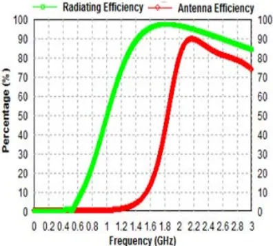
Microstrip antennas are used for various wireless applications due to their attractive features such as low profile, directive, high transmission frequency, low fabrication cost, light weight, conformal and planner structure and ease of integration with microwave circuit [1]. However microstrip antenna has a drawback of low bandwidth and low gain. The bandwidth can be increased by cutting slots and stacking configuration and Gain can be increased by using different patch elements in an array to achieve maximum radiation characteristics [1]. In this design of microstrip antenna a conducting patch is formed on a dielectric sheet of glass epoxy having dielectric constant of 4.2 and ground plane is formed on the back side of the sheet. In this antenna design the return loss bandwidth achieved 31.84% and maximum radiation efficiency obtained 95%.
II. PROPOSEDANTENNADESIGN
Following steps will be taken to design a rectangular microstrip patch antenna.
Step1: Calculation of width (W):
The width of the microstrip patch antenna is given by the equation as
Step2: Calculation of effective dielectric constant (
ε
reff):Step4: Calculation of actual length of patch (L): The following equation gives the length of patch as
Step5: Determination of feed point location (Xf ,Yf):The center of the patch is taken as the origin and feed point location is given by the coordinates (Xf ,Yf) from the origin. The feed point must be located at that point on the patch, where the input impedance is 50 ohms for the resonant frequency. Hence a trial and error method is used to locate the feed point. For different location of the feed point, the return loss (RL) is compared and that feed point is selected where the RL is most negative.
Fig. 1 Layout and structure of proposed antenna
For ground we use following relations:
Lg = L+6h = 24+6×1.6 = 33.6mm
PARAMETERS VALUES
DESIGN FREQUENCY 3GHZ
DIELECTRIC CONSTANT (GLASS EPOXY) 4.2
THE THICKNESS OF THE SUBSTRATE (H) 1.6 MM
WIDTH OF THE GROUND(WG) 40.6MM
LENGTH OF THE GROUND(LG) 33.6MM
WIDTH OF THE PATCH(W1) 31 MM
LENGTH OF THE PATCH(L1) 24 MM
W2 27 MM
L2 2 MM
W3 5 MM
L3 9 MM
W4 4 MM
III.RESULTSANDDISCUSSION
The resonant properties of the proposed antenna have been explained and optimised using IE3D software. The proposed antenna is tested by spectrum analyser and measured & simulated return loss of the proposed antenna is shown in figure 5 which are in good agreement
The simulated patch antenna gives bandwidth of 31.84% (2.075 to 2.861 GHz) at -10 dB return loss while the measured bandwidth of 30.33% (1.99 to 2.761 GHz) is achieved.
Various results from the analysis of the patch by giving the feed point location x = 17 mm and y = 35.2 mm are shown in figures.
Fig. 2 Return loss graph of proposed antenna
Fig 4 shows the Smith chart versus frequency plot shows the input impedance which should be ideally 50Ω.
Fig 5 shows the graph of VSWR. The minimum value of VSWR is about 1.6 at 2.21 GHz. The value of VSWR should be less than 2 for desirable communication.
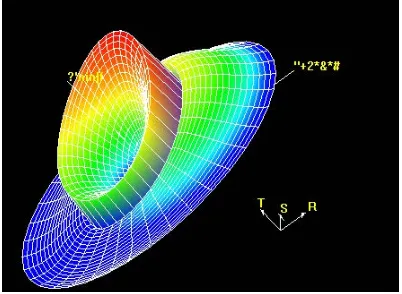
Fig 6 & 7 shows the 3D radiation pattern and 3D view of proposed antenna.
Fig. 3 Radiation and antenna efficiency graph of proposed antenna
Fig. 4 Smith chart of proposed antenna.
Fig. 5 Photograph of proposed antenna.
Fig. 6 3D Radiation pattern of proposed antenna.
Fig.7 3D view of proposed antenna.
CONCLUSIONS
A wideband inset feed microstrip patch antenna has been designed for high-speed wireless communication systems. The return loss bandwidth is measured 31.84% below −10 dB from 2.075 to 2.861 GHz frequency band. The maximum radiation efficiency is achieved 95%.The antenna is thin and compact with the use of low dielectric constant substrate material. The proposed geometry is designed using glass epoxy as a dielectric between the ground plane and patch
.
These features are very useful for portability of wireless communication equipment.REFERENCES
[1] A. Balanis, “Antenna Theory analysis and design”, Microstrip Antenna, Chapter 14, pp.720-784.
[2] Zakir Ali, Vinod Kumar Singh and Shahanaz Ayub, “Broad Band Slotted Stacked Microstrip Antenna for Wireless Applications”, International Journal of Advanced Research in Computer Science and Software Engineering Vol.2,No. 2, February 2012.
[3] Zakir Ali, Vinod Kumar Singh, Ashutosh Kumar, Ayub Shahanaz, “E shaped Microstrip Antenna on Rogers Substrate for WLAN applications” Proc. IEEE, pp.342- 345, Oct. 2011.
[4] A. M. Hadian, H.R. Hassani, “Wideband Rectangular Microstrip Patch Antenna with U-Slot”, IEEE, Electronics letters, vol. 33, No. 25, April. 2009.
[5] Amit A. Deshmukh and K. P. Ray, “Compact Broadband Slotted Rectangular Microstrip Antenna ”, IEEE antennas and wireless propagation letters, vol. 8, No. 3, March 2009, PP.377-382.
[6] B.K. Ang & B.K. Chung “A wideband E shaped Microstrip patch antenna for 5-6 GHz Wireless communications “PIER,75, pp. 397-407, 2007.
[7] Shivnarayan and Babau R. Vishvakarma, “Microstrip Patch Antenna with Inclined Slot for Dual-Band Operation”, Electronic letters, Vol. 33, No. 22, February 2006, PP.1833-1834.
[8] C.Y. Chiu, C.H. Chan and K.M. Luke, “Study of slotted microstrip patch antennas with folded patch fee ”, Microwave Antennas propagation., vol. 152, No. 5, October 2005.
IEEE Trans. Antennas Propagation , vol. 49, No. 1, 2001 pp. 45-47.
[13] Aaron Shackelford46, Kai-Fong Lee, Deb Chatterjee, “On Reducing the Patch Size of U-Slot and L-Probe Wideband Patch Antennas ”, IEEE Electronics Letters, Vol. 34 , 1998 , pp.1442-1443.
[14] S. K Satpathy, Vijay Srinivasan, K P Ray and G Kumar, “Compact microstrip antennas for personal mobile Comm.”, IEEE proc. pp. 245-248, 1998.