Abstract — Optimal design of LCL filter for grid connected inverter system is studied. For that, initially normal design is considered. Higher order LCL filters are essential in meeting the interconnection standard requirement for grid-connected voltage source converters. The IEEE 1547-2015 specifications for high-frequency current ripple are used as a major constraint early in the design to ensure that all subsequent optimizations are still compliant with the standards. The choice of switching frequency for pulse width modulation single-phase inverters, such as those used in grid-connected photovoltaic application, is usually a tradeoff between reducing the total harmonic distortion (THD) and reducing the switching loss. The total inductance per unit of the LCL filter is varied, and LCL parameter values which give the highest efficiency while simultaneously meeting the stringent standard requirements are identified. Then the conduction and switching losses that are caused by the filter are calculated and are optimized considering the level of reduction of harmonics. Hence the main aim of the study is to attenuate higher order harmonics along with the reduction in switching losses to ensure sinusoidal current injection into the grid. Further, the different switching schemes for single phase full bridge inverter are studied and compared to get the switching scheme which gives lesser switching losses. The LCL filter is designed accordingly and optimal inductance and capacitance values are obtained. Novel small signal model of a three phase grid connected VSI has been derived and its relevant transfer functions have been deduced from it so as to analyze the system for designing a controller and also bode plots have been plotted. Stability Analysis of Grid-Connected Inverters with an LCL Filter Considering Grid Impedance and comparative study between unipolar and bi-polar switching scheme for grid-connected inverter system is also done. Simulation is done in MATLAB SIMULINK environment for feasibility of the study.
Index Terms — LCL filter, Total harmonic distortion, switching loss, Renewable Energy Sources.
I. INTRODUCTION
t present, there is an exponential rise in the power demand and to meet this demand the existing energy resources are not sufficient. And also these resources are depleting day- by-day. So there is an urgent need to develop the power generation from Renewable Energy Sources (RES) which provide a reliable alternative for the conventional energy sources Optimal design of LCL filter for grid interfaced distributed power generation
system is studied. For that, initially normal design is considered. Higher request LCL channels are crucial in gathering the interconnection standard necessity. The IEEE 1547-2015 determinations for high-frequency current ripple are utilized as a real imperative ahead of schedule in the outline to guarantee that all resulting improvements are still agreeable with the models. The output filter helps in reducing the harmonics in generated current caused by semiconductor device switching. There are various types of filters. The simplest one is the filter inductor connected to the inverter's output. But various combinations of inductor and capacitors like LC or LCL can be used. This project presents the modeling of the grid side inverter and proposes a control strategy for better synchronization of the RES to the grid. The Renewable Energy Sources are connected to the utility grid through a power electronic converter and a filter.
Fig.1.1 Block Diagram of Grid Connected System In Fig. 1 the RES may represent wind or solar panel, which generate either ac or dc. Its main aim is to extract maximum power from the RES. It may contain a boost converter to boost the voltage levels to match with that of the utility grid values. The control algorithms of input side converter include MPPT techniques to extract maximum power from RES at every point of time. The DC-link is used for providing constant dc input voltage to the grid-side converter. It contains a capacitor, Cdc for this purpose. The Grid-side Converter converts the dc power to ac and feed it to the utility grid. The main aim of this converter is to maintain constant dc-link voltage to keep the frequency and phase of output current same as grid voltage. In addition to the above main tasks, the grid-side converter also regulates local voltage and frequency, compensates the voltage harmonics and may does active filtering when required. Thus, to control the power injected into the grid, the control of grid-side converter is of utmost important. But the output current from the inverter contains harmonics. So to filter out these harmonics a filter is used at the output of the inverter. The LCL-filter is a third order filter having attenuation of 60db/decade for frequencies above full resonant frequency, hence lower switching frequency for the converter switches could be utilized. Decoupling between the filter and the grid connected inverter R.Raja1, Dr.C.Nagarajan2 V.Sudha3
Assistant Professor, Department of Electrical and Electronics Engineering, Muthayammal Engineering College, Salem-636111, Tamil Nadu, India1
Mr. R. Raja , Dr.C.Nagarajan Mrs. V.Sudha
Designing of LCL Filter and Stability Analysis
of a Three Phase Grid Connected Inverter
System
having grid side impedance is better for this situation and lower current ripple over the grid inductor might be attained. The LCL filter will be vulnerable to oscillations too and it will magnify frequencies around its cut-off frequency. Therefore the filter is added with damping to reduce the effect of resonance. Therefore LCL-filter fits to our application. In the interim, the aggregate inductance of the received LCL filter is much more diminutive as contrasted with the L filter. Commonly, the expense is lessened. Besides, enhanced dynamic execution, harmonic attenuation and decreased volume might be accomplished with the utilization of LCL filter. The conduction and switching losses that are caused by the filter are calculated and are optimized considering the level of reduction of harmonics.
Fig.1.2. Single Phase Circuit of an LCL Filter with Passive Damping
II. DESIGNOFTHELCLFILTER
The greater part of the configuration mathematical statements are communicated in per unit basis of the volt-ampere rating of the power converter. Single phase equivalent circuit of the LCL filter with passive damping is demonstrated in Fig.1.2. The line-to-neutral output voltage VLN is the base voltage, and the three-phase kilovolt-ampere rating is the base volt-ampere. The fundamental frequency of 50 Hz is the base frequency. The inverter yield voltage and current are spoken to by ui and ii, and the output voltage and current are spoken to by ug and ig. The switching frequency is spoken to by fsw (in hertz) or ωsw (in radians for every second). We are considering power grid as a perfect voltage source, i.e., zero impedance, and it is supplying a steady voltage/current just at the fundamental frequency. The LCL filter transfer function which influences the closed-loop system bandwidth in the grid-connected mode of operation is represented as 1 ( ) 2 1 F S sLF s L CF F (2.1) 1 ( ) 2 ( 1 2) 1 2 F S S L L S L L C (2.2) 1 r L Cp (2.3) 1 2 1 2 L L Lp L L (2.4) 1 2 L a LL (2.5) 1 2 ( 1) r aL Lp aL C (2.6)
Where, L1 Inverter side inductance & L2 Grid side inductance. Taking resonant frequency ωr constant, is derived at the minimum capacitance as follows,
0 c aL
(2.7)
Whose simplification gives aL=1. . In this way, the most modest capacitance estimation of the LCL filter is gotten when L1=L2. Equation (2.3) becomes 4 2 r LC (2.8) After solving equation (2.2) and (2.4).We get.
1 2 1 2 L sw ig sw ui wr (2.9)
It gives the base L=L1+L2 per unit that will fulfill the standard suggestions for current ripple at the obliged switching frequency.
A. Passive Damping Scheme
The real target of damping is to decrease the Q-element at the resonance frequency without influencing the frequency response at different frequencies. The aggregate power dispersal in the damping circuit is additionally an imperative parameter to be considered.
1 2
L L
1
cd a cc and cc1cd (2.10) Where, Cd is the damping capacitor.
The required transfer function is
( ) 0.5 0.5 2 2 ( ) 1 1 1 2 2 1 uc j j C Rd d ui j sw sw j Rd ac wr wr (2.11) 1 1 2 1 ac j r dR ac Qc ac j r dR ac (2.12) L Rd C (2.13) Where, Rd is the damping resistor.
B. Power Losses
Power losses are calculated at fundamental frequency and switching frequency. Inductor: Essentially, losses in inductor are separated into core and copper loss. In spite of the fact that, there are some extra losses which are unimportant. So with the assistance of Magnetic design software both core and copper losses at switching and fundamental frequencies are ascertained and Damping Circuit and Capacitor.
C. Fundamental Frequency Power Loss
At fundamental frequency (50 Hz), the grid voltage is same as that of the voltage across the damping circuit (uc) Therefore,
2 2 2 50 (50) 2 2 2 1 50 uc C Rd d Pd C Rd d (2.12)
D. Switching Frequency Power Loss
At the switching frequency Grid is considered as a short circuited. However it is an ideal voltage source at fundamental frequency (50 Hz). So at switching frequency ug=0.Switching frequency power loss can be represented as
2 2 2 ( ) 2 2 2 2 2 1 ui sw C a b d Pd sw x C R c d sw d d (2.13) xsw d dC R
E. Total Loss in the LCL Filter
Complete losses incorporates core and copper loss both of every single part of filter. We can ascertain the base Lpu and Cpu that is obliged to meet the determinations of current harmonics for the converter appraisals defined in Table 2.1.
TABLE 2.1
CONVERTER RATINGS USED FOR CALCULATIONS
KVA Vbus Ibus f1 fsw fr Vdc
Kva V A Hz KHz KHz V
10 239.6 13.91 50 10 1 861
Communicating all qualities in per unit of the base rating detailed by Table 2.1 and utilizing mathematical equation (2.5) Lpu =0.015 & Cpu=0.661.
In this section we talked about the Ideal estimation of inductance and capacitance of LCL channel is ascertained. LCL parameter values which give the most astounding effectiveness are recognized by fluctuating the aggregate inductance for every unit of the LCL filter, while at the same time meeting the stringent standard necessities. Then the conduction and switching losses that are caused by the filter are calculated and are optimized considering the level of reduction of harmonics. Hence the main aim of the study is to attenuate higher order harmonics along with the reduction in switching losses to ensure sinusoidal current injection into the grid.
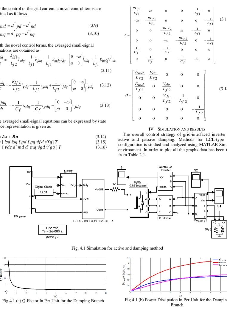
III. MODELLINGOFGRIDCONNECTEDINVERTER A small signal model of a three phase grid connected VSI has been derived and its relevant transfer functions have been deduced from it so as to analyze the system for designing a controller and also bode plots have been plotted. The averaged small-signal equations are expressed in state space representation which helps in analysis of stability of the overall system. To derive the averaged small-signal model, there are the processes composed of averaging, perturbing and linearizing step about the circuit equations. Fig. 3 is the circuit schematic of 3P-GC-3L-NPC inverter system with a LCL filter. The circuit equation is derived as follows.
Fig.3.1 Grid-connected three-level NPC inverter With a LCL filter 1disph 1 Vph Lf RLf sphi Vfph Vn dt 2digph 2 Vfph Vn Lf RLf igph Vgph dt (3.1) di fph Cf isph igph dt (3.2) Averaged Model and DQ-Coordinate Transformation
0 1 1 1 0 2 1 1 disdq RLf isdq vfdq dpdq dndq vdc isdq dt Lf Lf Lf (3.3) 0 1 1 2 0 2 2 2 digdq RLf igdq vgdq vfdq igdq dt Lf Lf Lf (3.4) 0 1 1 0 dv fdq isdq igdq vfdq dt Cf Cf d mq d pq d nq (3.5)A. Perturbed and Linearized Model
The perturbed values added to the small-signal ac variation (ˆ) around the operating dc point. After the linearization step neglecting nonlinear high-order ac terms, the averaged small-signal equations are obtained as
0 1 1 1 1 0 2 1 1 1 disdq RLf îsdq vfdq dmdq dcv îsdq DmdqV dc dt Lf Lf Lf Lf 0 1 1 2 0 2 2 2 digdq RLf igdq vgdq vfdq igdq dt Lf Lf Lf (3.7) 0 1 1 0 dv fdq isdq igdq vfdq dt Cf Cf (3.8)
For the control of the grid current, a novel control terms are defined as follows
dmd dpd dnd (3.9) dmqdpqdnq (3.10) With the novel control terms, the averaged small-signal equations are obtained as
0 1 1 1 1 0 2 1 1 1 disdq RLf îsdq vfdq dmdq dcv îsdq DmdqV dc dt Lf Lf Lf Lf (3.11) 0 1 1 2 0 2 2 2 digdq RLf igdq vgdq vfdq igdq dt Lf Lf Lf (3.12) 0 1 1 0 dv fdq isdq igdq vfdq dt Cf Cf (3.13)
The averaged small-signal equations can be expressed by state space representation is given as
𝒙̇ = 𝑨𝒙 + 𝑩𝒖 (3.14) 𝒙̇ = [ 𝑖̂𝑠𝑑 𝑖̂𝑠𝑞 𝑖̂ 𝑔𝑑 𝑖̂ 𝑔𝑞 𝑣̂𝑓𝑑 𝑣̂𝑓𝑞] 𝑻 (3.15) 𝒖 = [ 𝑣̂𝑑𝑐 𝑑 ̂ 𝑚𝑑 𝑑 ̂ 𝑚𝑞 𝑣̂𝑔𝑑 𝑣 ̂𝑔𝑞 ] 𝑻 (3.16) 1 1 0 0 0 1 1 1 1 0 0 0 1 1 1 2 0 0 0 2 1 1 2 0 0 0 2 1 1 1 0 0 0 1 1 0 0 RL f Lf Lf RL f Lf Lf RL f Lf Lf A RL f Lf Lf Cf Cf Cf Cf (3.17) 0 0 0 2 2 0 0 0 2 2 1 0 0 0 2 2 1 0 0 0 0 2 0 0 0 0 0 Dmd Vdc Lf Lf Dmd Vdc Lf Lf B Vdc Lf Lf L f (3.18)
IV. SIMULATION AND RESULTS
The overall control strategy of grid-interfaced inverter with active and passive damping. Methods for LCL-type filter configuration is studied and analyzed using MATLAB Simulink environment. In order to plot all the graphs data has been taken from Table 2.1.
Fig. 4.1 Simulation for active and damping method
Fig 4.1 (c) Core Loss Variation with the Inductance at Fundamental Frequency.
Fig 4.1 (d) Copper Loss Variation with the Inductance at Fundamental Frequency
Fig 4.1 (e) Normalized RMS Current Ripple Verses Ma From the figure 4.1, we can see that there is no change in the Q of the frequency response if AC is expanded past two. Along these lines, we are setting ac=1as the best decision, since it is essentially simple to design two capacitors of the same worth.
Fig 4.1 (f) Control to Converter Current Transfer Function Bode Plot for Active Damping
Fig 4.1 (g) Control to Grid Current Transfer Function Bode Plot for Passive Damping
Fig 4.1 (h) Control to Grid Current Transfer Function Bode Plot for Active Damping
Fig 4.1 (i) Time Variation of the Switching Frequency for Ma=0.95 and Φ =00.
Fig 4.1 (j) Time Variation of the Switching Frequency for Ma=0.95 and Φ=Π/6.
Fig 4.1 (k) Switching Loss Saving Versus Φ For Ma=0.95.
Fig 4.1 (l) Nyquist Plots for the Eigenvalues of the Return-Ratio Matrix Ldq (S) Controlled with Converter-Side Current. The dissection demonstrated that for gathering the same THD prerequisite with a given filter, the ideal exchanging plan spares up to 36.5% under "best-case" conditions contrasted with the fixed switching frequency scheme. In Fig 4.1, the Nyquist diagram for 𝑙2(𝑠)is almost in the unit circle and does not intersect with the unit circle on the left plane of the complex plane. Whereas 𝑙1(𝑠) presents large magnitude and does not encircle about (-1, j0), it intersects with the unit circle on the left plane of the complex plane and it influences the stability margin of the system.
Fig 4.1 (m) Nyquist plots for 11(s) and l (s).
Fig 4.1 (n) Magnitude distribution of Δ𝑖𝑝𝑘−𝑝𝑘 bipolar switching
Fig 4.1 (o) Magnitude distribution of Δ𝑖𝑝𝑘−𝑝𝑘 unipolar switching scheme for 𝑚𝑎 = 0.8.
Fig 4.1 (p) |𝐻𝐿𝐶𝐿 | and |𝐻𝐿| versus Harmonic Number Fig. 4.1 shows the Nyquist plots for 𝑙1(𝑠) and 𝑙2(𝑠). Therefore, the resistive component in the grid impedance is able to improve the stability margin of the grid-connected system. In order to guarantee a sufficient stability margin for the system, this paper considers extreme cases and 𝑙(𝑠) is utilized to analyze the stability margin of system. Therefore, the stability analysis of a grid-connected system with an LCL filter is converted into a study of the d-d channel output impedance 𝑍𝑑𝑑 (𝑠) and the inductive component 𝑍𝐿𝑔(𝑠) in the grid impedance. Further, it is indicated that the steadiness of the grid-connected system controlled with the converter-side current is completely dictated by the d-d channel output impedance of the grid connected inverter and the inductive part of the grid impedance and the stability margin of the grid-connected inverter can be changed by regulating the LCL parameters. Fig 5.16 shows the plot of |𝐻𝐿𝐶𝐿 | and|𝐻𝐿| | versus harmonic order with X= 0. 001 for every unit, Xc=2 for every unit and Xg = X/5. It might be unmistakably seen that the LCL filter has better constriction especially at frequencies over the 50th harmonic.
V. CONCLUSION
Optimal LCL filter design along with switching loss reduction is presented. Hence, the optimal filter is designed considering THD% and ripple factor. And for that value of inductor different switching losses are studied. The analysis showed that for meeting the same THD requirement with a given filter, the optimal switching scheme saves up to 36.5% under “best-case” conditions compared to the fixed switching frequency scheme. Thus, using this scheme can reduce the size of the heat sink or, for an existing heat sink design, reduce the temperature of the switches and possibly extend the inverter life. The total LCL filter loss per phase was plotted. These loss curves were used to find the most efficient LCL filter design. A frequency-domain
analysis to design the control systems, system stability and the control scheme of the grid current based on the averaged small-signal model is studied. The resistive component in the grid impedance is able to improve the stability margin of the grid-connected system.
VI. REFERENCES
[1] Connected Converters Basic Criteria in Designing LCL Filters for Grid Connected Converters” , IEEE ISIE 2006, July 9-12, 2006, Montreal, Quebec, Canada.
[2] Karshenas, H.R.; Saghafi, H., "Performance Investigation of LCL Filters in Grid Connected Converters," Transmission & Distribution Conference and Exposition: Latin America, 2006. TDC '06. IEEE/PES , vol., no., pp.1,6, 15-18 Aug. 2006
[3] P. Daly and J. Morrison," Understanding the Potential Benefits of Distributed Generation on Power Delivery," IEEE Rural Electric Power Conference, 2001
[4] J. F. Manwell, et al, Wind Energy Explained, John Wiley & Sons Ltd., 2002.
[5] M. Liserre, F. Blaabjerg, and S. Hansen "Design and Control of an LCL-Filter-Based Three-Phase Active Rectifier," IEEE Trans. Industry Applications, vol. 41, no. 5, pp. 1281-1291, September/October 2005.
[6] M. Lindgren and J. Svensson," Control of a Voltage-source Converter Connected to the Grid through an LCL-filter-Application to Active Filtering," in Proc. PESC'98, vol. 1, 1998, pp. 229-235.
[7] M. Lindgren and J. Svensson," Current Control of Voltage Source Converters connected to the grid through an LCL-filter," in Proc. PESC'04, vol. 1, 2004, pp. 125-132.
[8] Channegowda, P.; John, V.; , "Filter Optimization for Grid Interactive Voltage Source Inverters," Industrial Electronics, IEEE Transactions on, vol.57, no.12, pp.4106-4114, Dec. 2010.
[9] Jiri Lettl, Jan Bauer, and Libor Linhar; “Comparison of Different Filter Types for Grid Connected Inverter”, PIERS Proceedings, Marrakesh, MOROCCO, March 20-23, 2011. [10] Yibin Tong, Fen Tang, Yao Chen, Fei Zhou, and Xinmin
Jin; “Design Algorithm of Grid-side LCL-filter for Three-phase Voltage Source PWM Rectifier”, J. A. Ferreira, “Improved analytical modelling of conductive losses in magnetic components,”IEEE Trans. Power Electron., vol. 9, no. 1, pp. 127–131, Jan. 1994.
[11] M. Bartoli, A. Reatti, and M. K. Kazimierczuk, “Modelling winding losses in high frequency power inductors,” J. Circuits, Syst. Comput.,vol.5,no. 4, pp. 607–626, Dec. 1995. [12] Xiaolin Mao; Ayyanar, R.; Krishnamurthy, H.K.; , "Optimal
Variable Switching Frequency Scheme for Reducing Switching Loss in Single Phase Inverters Based on Time-Domain Ripple Analysis," Power Electronics, IEEE Transactions on , vol.24, no.4, pp.991-1001, April 2009. [13] Erickson. RW, fundamental of Power Electronics; Norwell
MA, Kluwer, 1997.S
[14] Xiao-Qiang Li, Xiao-Jie Wu, Yi-Wen Geng, and Qi Zhang; “Stability Analysis of Grid-Connected Inverters with an LCL Filter Considering Grid Impedance”, Journal of Power Electronics, Vol. 13, No. 5, September 2013.
[15] Hyosung Kim, Kyoung-Hwan Kim, “Filter design for grid connected PV inverters”, Proc. of IEEE International on Sustainable Energy Technologies, ICSET200), pp.1070-1075, 2008.
[16] Debati Marandi, Tontepu Naga Sowmya, and B Chitti Babu Member, IEEE; , “Comparative Study between Unipolar and Bipolar Switching Scheme with LCL Filter for Single-Phase Grid Connected Inverter System”, 2012 IEEE Students’ Conference on Electrical, Electronics and Computer Science.
Dr.C.Nagarajan has completed his B.E degree in K.S.Rangasamy College of Technology, and his M.Tech degree in Vellore Institute of Technology. He has been awarded Ph.D. degree in 2011 from Bharath Institute of Higher Education and Research University Chennai. He has about 12 years of teaching experience and he is currently working as Professor/ Head of Electrical and Electronics Engineering. He is also guiding 12 Ph.D. research scholars. He has published his research works in various International Journals and referred journals. His area of interest include Power Electronics & Drives, Intelligent Control Techniques.
R. Raja has received his B.E degree in Electrical and Electronics Engineering at Mahendra college of Engineering on 2011 and his M.E degree in Power Electronics and Drives from Sona College of Technology, Salem affiliated under Anna University on 2013. He is currently pursuing his Ph.D. in Electrical Engineering working as Assistant Professor in Muthayammal Engineering College., Rasipuram. He has published many papers in International journals.
V.Sudha has received her B.E degree in Electronics and Communication Engineering at Sona College of Technology, Salem on 2009 and her M.E degree in Applied Electronics and Drives at Regional centre of Anna University Coimbatore, affiliated under Anna University on 2012. She is currently working in Pavai College of Technology as Assistant Professor. She has published many papers in International journals.