3345 ISSN: 2278 – 7798 All Rights Reserved © 2015 IJSETR
Abstract— In this paper, an integrated two stage converter is
proposed as a high power factor offline driver for power LED lamps. The circuit uses two inductors and two capacitors as energy transferring elements which provides high quality, high efficient driver to the lamps. The advantage of this converter is that it uses only one MOSFET as switch. With a careful design of the converter, film capacitors may be used, thus avoiding low life-rating electrolytic capacitors in the whole converter. The main feature of this circuit is that have a galvanic isolation between the source and the load is provided. A design example for a 70W converter supplied from a 230V/50 Hz mains is shown.
Index Terms—Continuous Conduction Mode, Discontinuous
Conduction Mode, Duty Cycle, Electrolytic capacitors, film capacitors, LED driver, Pulse Width Modulation
I. INTRODUCTION
Nowadays the energy-inefficient incandescent lamps and mercury-based tubular and compact fluorescent lamps are replacing as LED lamps. In electronics, an LED circuit is an electrical circuit used to power a light-emitting diode (LED). The circuit must provide sufficient current to light the LED at the required brightness, but must limit the current to prevent damaging the LED. The voltage drop across an LED is approximately constant over a wide range of operating current; therefore, a small increase in applied voltage greatly increases the current. That is, an LED driver is a self-contained power supply that controls the amount of current and voltage supplied to an LED light. An LED constant current driver monitors the loop current of each LED and automatically adjusts the generated DC voltage output to the minimum value needed to produce the highest forward voltage. As mains power is Alternating Current (AC) and Light Emitting Diodes run on Direct Current (DC), this current needs to be converted by a rectifier. Some LED lamps have inbuilt rectifiers so can be used with iron-core transformers. If there is no inbuilt rectifier then the LED light needs to be used in conjunction with an LED specific driver as they all have rectifiers as standard. Some LED Drivers use Pulse Width Modulation (PWM) in conjunction to enable the LED light to become dimmable.
Very simple circuits are used for low-power indicator LEDs. More complex, current source circuits are required when driving high-power LEDs for illumination to achieve correct current regulation. As the technology improves,
Manuscript received September, 2015.
Aaliya P A, M Tech student, Electrical and Electronics Engineering, KMEA Engineering College, India.
Prof. George T V, Electrical and Electronics Engineering, KMEA
Engineering College, India.
numerous types of switching converters have been developed as power
supply to LEDs. The numerous types of switching converter include boost, buck, buck-boost, and Cuk converters. Here a two stage buck boost and fly-back converter is provided as a driver to the LED lamps which has high power factor, long life and high efficiency. The advantage of fly-back converter is providing isolation between input and load side.
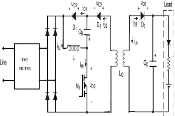
II. INTEGRATED TWO STAGE CONVERTER Fig-1 shows the electrical diagram of the Integrated Two stage Converter.
Fig -1: Integrated two stage converter
This converter is similar to two buck–boost converters in cascade. Li, D1, CB, and M1 form the input buck-boost converter and LO, D2, D3, CO, and M1 form the output buck-boost converter. A reversing polarity is produced by the first converter in the capacitor CB. It is corrected by the second converter, giving a positive output voltage with respect to ground.
Since the input inductor Li is operated in discontinuous conduction mode (DCM), the average current through the line will be proportional to the line voltage, giving a near unity power factor. The output inductance LO can be operated either in continuous conduction mode (CCM) or DCM. Although the operation in DCM has the advantage of providing a bus voltage across CB independent of the duty cycle and output power, it presents the disadvantage of requiring a higher value of the output capacitance Co to achieve low current ripple through the load. Because the current ripple is lower in CCM, the output inductance Lo is operated in this mode to have a reduced value for Co.
Integrated Two Stage LED Driver
The operation of the fly-back stage in CCM with a duty cycle lower than 0.5 reduces the low-frequency ripple voltage since it is multiplied by the buck–boost converter voltage ratio. Thus, it will be possible to use a film capacitor to implement Co, thus having a higher life rating and better efficiency than using electrolytic capacitors.
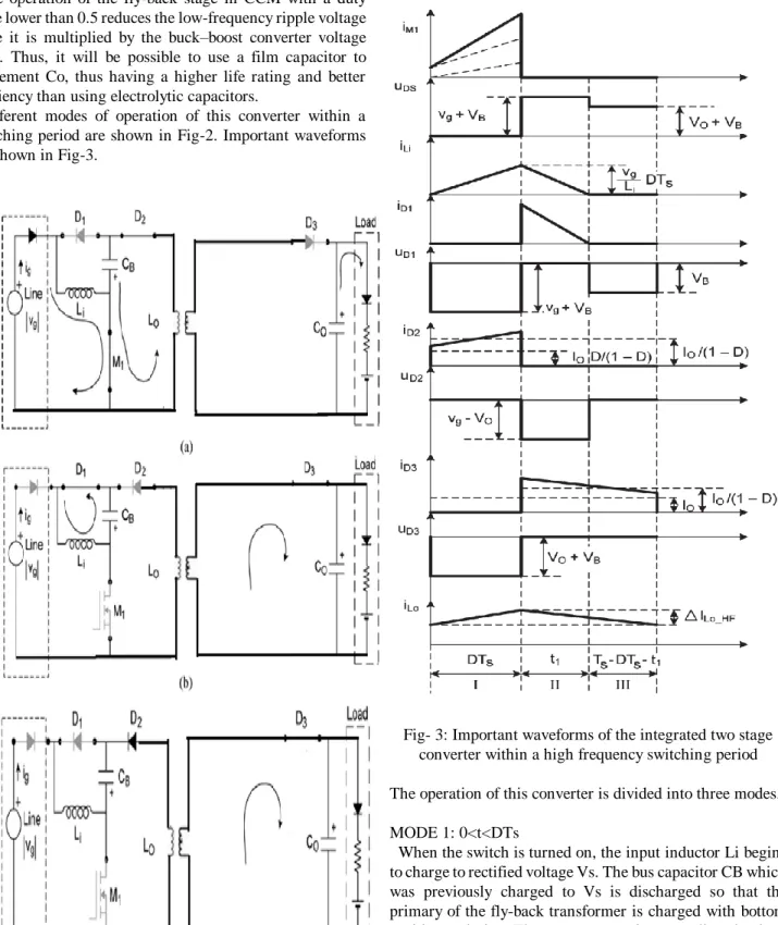
Different modes of operation of this converter within a switching period are shown in Fig-2. Important waveforms are shown in Fig-3.
Fig- 2: Different modes of operation of the Integrated two stage Converter (a) Mode I: 0<t<DTs (b) Mode II : DTs <t
<DTs+t1 (c)Mode III : DTs+t1< t<Ts
Fig- 3: Important waveforms of the integrated two stage converter within a high frequency switching period The operation of this converter is divided into three modes. MODE 1: 0<t<DTs
When the switch is turned on, the input inductor Li begins to charge to rectified voltage Vs. The bus capacitor CB which was previously charged to Vs is discharged so that the primary of the fly-back transformer is charged with bottom positive polarity. The output capacitor supplies the load current.
MODE 2: DTs<t<DTs+t1
When the switch is turned off, Li is discharged through diode D1. Opposite polarity voltage is induced in the secondary of the fly-back transformer so that the diode D3 is forward biased and it supplies the load. At the end of this mode, Li is completely discharged.
MODE 3: DTs+t1<t<Ts
There will be no current flow in the input side. Since diode D3 is forward biased, the secondary of the fly-back transformer still supply the load.
3347 ISSN: 2278 – 7798 All Rights Reserved © 2015 IJSETR
III. ANALYSIS AND DESIGN OF INTEGRATED TWO STAGE CONVERTER
In this section, an integrated two stage converter is analysed when operated from the main voltage and a simulation prototype has been developed using MATLAB/SIMULINK. Considering the lamp formed by 60 LW W5SG power LEDs by Osram in a series array, the load rating current is 350 mA, with an output power of 70W and a total luminous flux of 1500 lm. The load was tested at the laboratory to obtain the following model parameters: V = 170 V and R= 87 Ω [4]. The equivalent load resistance at nominal power is R = 577. The selected switching frequency is 50 kHz. The line voltage is 230 Vrms with a 50-Hz line frequency. The converter must admit at least 10% line voltage variation, assuring constant current through the load.
Let the line voltage be a sinusoidal waveform given as
t
V
t
v
L g g(
)
sin
(1) A. Line current and Input powerThe current ig is the input current through Li during the time interval 0-DTs, and is modulated by the rectified line voltage as shown in Fig-5, where D is the transistor duty cycle and Ts is the switching period.
Fig- 5: Input Current Waveform
The input current averaged at line frequency can be calculated as
t
Sin
f
L
V
D
DT
i
T
i
L S i g S peak g S g
2
2
1
1
2 _
(2)where ig_peak is the instantaneous peak current in each switching period, Vg is the peak line voltage, fs is the switching frequency and ɷL is the line angular frequency. Thus ig is a sinusoidal waveform that will provide an input power factor close to unity.
Taking into account that both input waveforms are sinusoidal, the average input power Pg can now be calculated as,
f
L
V
D
i
V
P
S i g peak g g g4
2
1
2 2
(3) where <ig>peak is the averaged input current peak value. B. Output voltage and Bus voltageThe output power Po is
R
V
P
O o 2
(4) where Vo is the output voltage and R is the static equivalent resistance of the LED load, which is obtained by the ratiobetween the LED voltage and current dc values at each operating point.
R
I
V
I
I
R
V
I
V
R
LED LED LED LED LED
(5) where Vγ and Rγ are the voltage and resistance parameters of the LED lamp equivalent circuit.The output voltage Vo for the ideal converter is calculated by equaling input power Pg and output power Po. Assuming 100% efficiency, by equating equations 3 and 4, Vo is finally obtained as
K
V
D
V
g O2
(6)where K is a non dimensional factor given by R
L
f
K
S i
(7) The bus voltage VB can be calculated by using the voltage conversion ratio for this converter.K
V
D
V
D
D
V
B O g 2)
1
(
1
(8)The limit duty cycle Dlimit can be obtained from the voltage
conversion ratio in the DCM-CCM boundary
V
V
D
B g it
1
1
lim (9) When the actual duty cycle is lower than the limit value, the input stage will operate in DCM.C. Reactive components
The input inductance Li can be obtained using equation 3and assuming 100% efficiency
(10)
By choosing a duty cycle of 40%, a value Li =1.2 mH is obtained. Now, Li is selected to be 0.4 mH when the operation of Li in discontinuous mode for the whole line voltage range is checked.
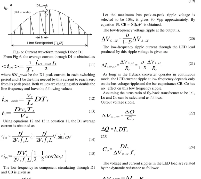
The bus capacitor CB is the voltage applied to the second stage. The current through this capacitor is given by the currents through diodes D1 and D2. In these diodes, only the current through D1 is modulated by a rectified line frequency, as shown in Fig-6. In order to calculate the bus ripple, the low frequency component of the current through D1 must be obtained.
f
P
V
D
L
S O g i4
2 2 Fig- 6: Current waveform through Diode D1 From Fig-6, the average current through D1 is obtained as
2 1 1_ 1 1
t
i
T
i
D peak S D
(11) where iD1_peak be the D1 peak current in each switching period and t1 be the time needed by this current to reach zero from its peak point. Both values are changing after double the line frequency and have the following values:DT
L
v
i
S i g peak D1_
(12)V
T
Dv
t
B S g
1 (13)Using equations 12 and 13 in equation 11, the D1 average current is obtained as
(14)
(15) The low-frequency ac component circulating through D1 and CB is given as
(16)
Now, the low-frequency peak-to-peak ripple voltage across capacitor CB,
V
LF B
_ can be obtained as,X
i
V
B_LF
2
D1
ac_peakC
B
(17)C
f
L
f
V
V
D
B L i S B g ) ( 2 12
4
2
2 2
f
f
C
L
V
V
D
L S B i B g
8
2 2 (18)where
i
D1
ac_peak is the peak value of the low-frequency current through diode D1, obtained from equation 16, and fL is the line frequency. The necessary bus capacitance is then calculated from equation 18 as follows(19)
Let the maximum bus peak-to-peak ripple voltage is selected to be 10%; it gives 30 Vpp approximately. By equation 19, CB =
80
F
is obtained.The low-frequency voltage ripple at the output is,
V
V
O LFD
B LFD
_ _1
(20)The low-frequency ripple current through the LED load produced by this ripple voltage is given as:
R
V
R
V
I
LED LF O LF B LF D D
_ _ _ 1 (21) As long as the flyback converter operates in continuous mode, the LED current ripple at low frequency depends only on the bus voltage ripple and the bus capacitance CB. Co has no effect on this low frequency ripple.Assuming the turns ratio of fly-back transformer to be 1:1, Lo and Co can be calculated as follows.
Output voltage ripple,
C
Q
V
O HF O
_ (22)DT
I
Q
O S
(23)f
V
DI
C
S HF O O O
(24)The voltage and current ripples in the LED load are related by the dynamic resistance as follows:
(25)
Using equation 25 in 24, Co =
40
F
is obtained for a .2% current ripple at high frequency.Average current through Lo,
I
I
I
D D LO 2 3
(26)D
I
I
D
D
I
o O O
1
1
(27)Taking average voltage across Lo=0,
V
DT
I
L
B S O D
2 (28) (4.27) t L g i S B g i S B DV
L
f
V
D
v
L
f
V
D
i
sin
2
2
2 2 2 2 2 1 t
L
f
V
V
D
i
L i S B g Dcos
2
2
1
2
1
2
2 2 1t
L
f
V
V
D
i
L i S B g ac Dcos
2
2
2 2 1
V
LED
I
LEDR
3349 ISSN: 2278 – 7798 All Rights Reserved © 2015 IJSETR
V
t
I
L
O off O D
3 (29)f
L
V
D
I
I
I
S O B D D LO HF2
3 _ 2
(30) (31)where ΔILo_HF is the high-frequency peak-to-peak current ripple, ΔVo_HF is the high-frequency peak-to-peak output voltage ripple, and Io is the dc current through the LED load. Selecting a maximum ripple voltage of 4.2%, this is around 10 Vpp. Lo is calculated for a 50% current ripple. Using equation 31, a value Lo = 7 mH is obtained.
An EMI filter is formed by a 20-mH common-mode inductance and a 2-mH differential-mode inductance with two 100 nF across the input and the output of the filter [1]. The filter was used to avoid high-frequency current circulating through the line and to avoid distortion in the input current.
IV. SIMULATION
Simulation is done in MATLAB/SIMULINK.
The simulation diagram of integrated two stage converter is shown in Fig-7. A buck boost converter operating in discontinuous mode provides the required power factor correction. In order to provide the dc voltage regulation as well as the galvanic isolation a fly-back converter is placed in the output stage. The operation of fly-back converter is similar to that of buck boost converter.
V. VI. VII. VIII. IX. X. 3.3 SIMULATION RESULTS A. Simulation results
From Fig- 8, it is observed that the input current is almost sinusoidal and follows the input voltage. The power factor therefore is very high of about 99 %.
XI. XII. XIII. XIV. XV.
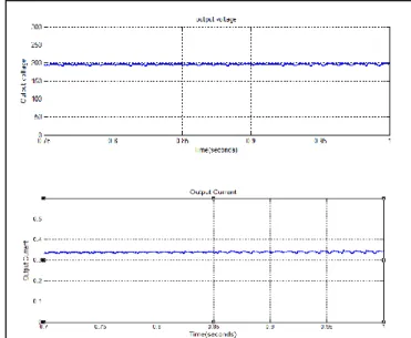
The output voltage and current are almost steady at about 200V and 0.35A respectively. This can be seen from Fig- 9. From the figure, it can be seen that there is certain ripple in the output voltage and current; actually it can be deliberately added in order to reduce the value of capacitance and make use of film capacitors.
f
I
DV
L
S B O LO HF
_2
Fig- 7: Simulated Integrated Two stage Converter
Fig- 8: (a) Input Voltage (b) Input Current
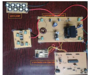
V. EXPERIMENTAL SETUP
Due to practical difficulties of making the hardware section of the LED driver with EMI filter, here an integrated two stage converter is experimentally verified without EMI filter. The output voltage is maintained to be 24 V. The switching frequency is 50 KHz.
The experimental set up is shown in Fig-10. There are basically three sections for the circuit; the converter section, controller section and the load LED matrix. It also consists of regulator IC LM 317 to provide the Vcc to dsPIC and MOSFET gate driver IC.
The converter circuit consists of the cascaded buck boost circuit. Supply is taken from mains and it has a diode bridge rectifier to obtain dc input to the converter circuit. dsPIC is used to shape the gate pulses which is given to the gate of MOSFET through gate driver IC. The output voltage is fed back to the feedback circuit which provides the analog pulse to the ADC input of dsPIC. Also this circuit is provided with regulator IC to provide the required voltage to gate driver IC and dsPIC. The load consists of 8 LEDs in series with the rating 3 V and 1 W. So the current through the load is 0.33A and voltage across it is 24V.
A. Experimental Results
The source voltage and input current of the system is shown in Fig-11. Here the line voltage can be varied up to 70 V rms. If the voltage is greater than this, then the switching losses will increase and the output voltage decreases. The distortion in the input can be reduced using an EMI filter in the input. But it increases the complexity of the circuit. From the figure, we can see that input current and voltage are in phase. Hence the input power-factor is very high.
Fig-12shows the gate pulse to the switch. This is of 50 KHz frequency. The duty cycle is regulated to get the required voltage in the output.
From Fig- 13, it can be seen that the output voltage is obtained to be 24 V. Certain ripple in the output can be deliberately added in order to reduce the value of output capacitance.
VI. CONCLUSIONS
The main thrust of the thesis is to provide a highly efficient driver for power LED lamps with high power factor. Since the input buck-boost stage is operating in DCM, it has got Fig- 11: Source voltage and Input Current of the
Fig- 12: Gate pulse to the switch Fig- 10: Experimental Setup
3351 ISSN: 2278 – 7798 All Rights Reserved © 2015 IJSETR
very high power factor. This converter can stably maintain the output voltage and current to the required level. The closed loop control is implemented using a microcontroller. With a careful design of the converter, the bus capacitor can be made low and thus it is possible to use film capacitors, which reduces the size, weight and cost of the circuit, thus avoiding the low-life-rating electrolytic capacitors in the whole converter.
By providing fly-back converter, it can be used for medical applications where isolation is essential. Though isolation increases the cost, it is a safety aspect that cannot be neglected in certain applications.
In this paper, the converter was implemented to obtain only one lighting level. It can be extended for street lighting application where more than two lighting levels are used. The low dimming level can be implemented by reducing mean current through the LED lamp.
REFERENCES
[1] J. Marcos Alonso, Senior Member, IEEE, Juan Viña, ―Analysis and Design of the Integrated Double Buck–Boost Converter as a High Power Factor Driver for Power-LED Lamps‖, IEEE Trans.Industrial Electronics, Vol. 59, no. 4, April 2012, 1689—1697
[2] Mel Berman TDK‖All about EMI filters‖, ELECTRONIC PRODUCTS , October 2008
[3] Fu-Yuan Shih, Dan Y. Chen, Yan-Pei Wu, Yie-Tone Chen,‖ A Procedure for Designing EMI filters for AC applications‖, IEEE TRANSACTIONS ON POWER ELECTRONICS, VOL.11 NO. , JANUARY 1996
[4] D. Gacio, J. M. Alonso, A. J. Calleja, J. Garcia, and M. Rico-Secades, ―A universal-input single-stage high-power-factor power supply for HB-LEDs based on integrated buck-flyback converter,‖ IEEE Trans. Ind.Electron., vol. 58, no. 2, pp. 589–599, Feb. 2011
Aaliya P A was born in Kerala, India in 1990.She received the B.Tech degree in electrical engineering from Mar Athanasius College of Engineering, Kothamangalam, Kerala in 2012. She is currently doing Post Graduation from KMEA Engineering College, Edathala, Kerala.
Prof. George T V received the B. Tech and M. Tech degrees from National Institute of Technology, Calicut, Kerala and had been working with Neyveli Lignite Corporation Limited. Currently he is a professor in the KMEA Engineering College, Kerala, India