Temperature Dependent Current-Voltage and Capacitance-Voltage Characteristics
of an Au
/
n-Type Si Schottky Barrier Diode Modi
fi
ed Using a PEDOT:PSS Interlayer
Zagarzusem Khurelbaatar
1, Kyu-Hwan Shim
1, Jaehee Cho
1, Hyobong Hong
2,
V. Rajagopal Reddy
3,+and Chel-Jong Choi
1,+1School of Semiconductor and Chemical Engineering, Semiconductor Physics Research Center (SPRC), Chonbuk National University, Jeonju 561-756, Republic of Korea
2IT Convergence Technology Research Laboratory, Electronics & Telecommunication Research Institute, Daejeon 306-700, Republic of Korea
3Department of Physics, Sri Venkateswara University, Tirupati-517 502, India
The temperature dependence of the current-voltage (I-V) and capacitance-voltage (C-V) characteristics of an Au/n-type Si Schottky barrier diode (SBD) with a PEDOT:PSS interlayer was investigated. The SBD parameters, such as Schottky barrier height ()B), ideality factor (n),
saturation current (I0), doping concentration (ND), and series resistance (Rs), were obtained as a function of temperature. The Richardson constant
(A**) obtained from the In(Io/T2) versus 1000/Tplot was much less than the theoretical value for n-Si. The mean Schottky barrier height (bo)
and standard deviation (·0) calculated using the apparent Schottky barrier height ()ap) versus 1/2kTplot were 1.26 eV and 0.15 eV, respectively.
From afit of the modified Richardson plot of ln(I0/T2)¹(q·)2/2(kT)2versus 1000/T, theA**was extracted as 134 A/cm2K2, which was close
to the theoretical value of the n-Si. The interface state densities obtained from the Au/PEDOT:PSS/n-Si SBD decreased with increasing temperature. Furthermore, the conduction mechanism dominating the reverse-bias leakage current in Au/PEDOT:PSS/n-Si SBD was described and discussed. [doi:10.2320/matertrans.M2014263]
(Received July 14, 2014; Accepted October 6, 2014; Published November 14, 2014)
Keywords: Schottky barrier diode, poly(3,4-ethylenedioxythiophene):polystyrene sulfonate (PEDOT:PSS), gaussian distribution, barrier inhomogeneity
1. Introduction
Schottky barrier diodes (SBDs) have received significant attention in the development of various electronic devices due to their low forward voltage drop and fast switching action. There are numerous reports on the theoretical and experimental studies of SBDs, but they continue to be extensively studied to fully understand the nature of the contact. The fabrication of high quality SBDs with a low ideality factor (n) using a thin interfacial layer is one of the essential prerequisites for electronic devices. Recent research has been performed by applying conducting polymer materials to SBDs as an interfacial layer by a solution based spin-coating process.13) It is found that performance,
reliability and stability of SBDs depends on various parame-ters such as the fabrication process, surface preparation, density of surface states distributed at the interface, device temperature and voltage, series resistance (RS) of the device,
thermal and mechanical stability of the polymer used. Among various conducting polymers, poly(3,4-ethylenedioxythio-phene):poly (styrene sulfonate) (PEDOT:PSS), one of the most important polymers, has recently received considerable interest because it exhibits a p-type semiconductor with a high work function (³5 eV), high conductivity (35300 S·cm¹1 at room temperature), good transparency (³95% at visible region), excellent photo-stability, and good environ-mental stability.4,5) Several research groups have used PEDOT:PSS as a Schottky junction with n-type Si sub-strates.610) According to previous reports, the electrical
transport properties of SBDs depend highly on the conditions
of the fabrication processes, such as the utilization of a particular solvent, the amount of PSS, the doping ratio of PEDOT in the PEDOT:PSS mixture, the uniformity of the PEDOT:PSS thin film, and the environmental conditions during the fabrication. As a result, there is a large variation in the electrical transport of PEDOT:PSS/n-Si SBDs. More-over, there is no experimental study done on their temper-ature-dependent electrical characteristics. Analysis of the current-voltage (I-V) and capacitance-voltage (C-V) charac-teristics of metal-semiconductor and metal-insulator-semi-conductor structures only at room temperature cannot provide detailed information regarding the current conduction mechanisms or the nature of the barrier formation at the metal-semiconductor interface.11) On the other hand, the temperature dependence of the I-V and C-V characteristics could allow us to gain insight into different aspects of characteristics such as nature of interfacial insulator layer and carrier conduction mechanism.
In this study, we fabricated Au/n-type Si SBDs with a PEDOT:PSS interlayer using spin-coating process and reactive ion etching process (RIE). For the electrical characteristics of the Au/PEDOT:PSS/n-Si SBDs, electrical transport measurement were investigated by bothI-VandC-V measurements in the temperature range from 200 to 400 K. The Schottky barrier height ()B),n, saturation current (I0),
doping concentration (ND), andRSof Au/PEDOT:PSS/n-Si
SBDs were extracted at different temperatures. The temper-ature dependence of the energy distribution of the interface state density (NSS) profile was determined based on the
variation of the ideality factor with forward bias and temperature. Temperature-dependent barrier characteristics of the Au/PEDOT:PSS/n-Si SBDs were also interpreted based on the existence of the Gaussian distribution of the +Corresponding author, E-mail: reddy_vrg@rediffmail.com, cjchoi@jbnu.
ac.kr
barrier heights. Furthermore, the possible current conduction mechanism of the Schottky contacts modified using the PEDOT:PSS interlayer was also studied.
2. Experimental Procedures
The n-type Si (100) wafers with a resistivity of 110³·cm were used as a starting material. The carrier density of Si substrate, measured by Hall measurement system, was extracted to be 1.21©1015cm3. After removing native oxide, the PEDOT:PSS layer was spin-coated on a cleaned n-Si wafer, followed by baking at 150°C in air. The scanning electron microscope examination (not shown here) revealed that the thickness of the PEDOT:PSSfilm was approximately 60 nm. In addition, the sheet resistance of PEDOT:PSSfilm spin-coated on insulating glass substrate, measured by the four-point probe, was found to be³2.6©103³/squre. The
top Au (100 nm) electrode with 1-mm diameter (area= 7.85©10¹3cm2) was formed on PEDOT:PSS film with a
metal mask by an e-beam evaporation system at a pressure of 3.99©10¹4Pa. The redundant PEDOT:PSS film was then removed by the O2 plasma RIE process and resulting in a
circular dot shaped Au/PEDOT:PSS electrode formed on n-Si. The GaIn paste was then applied to the backside of the n-Si wafer for ohmic contacts. The schematic cross section of the Au/PEDOT:PSS/n-Si SBD is shown in the inset of Fig. 1. The I-V and C-V measurements of the Au/ PEDOT:PSS/n-Si SBD were performed using a semicon-ductor parameter analyzer (Agilent Technologies, 4155C) and LCR meter (Agilent Technologies, 4284A) at a temper-ature range of 200400 K in steps of 40 K under a dark condition.
3. Results and Discussion
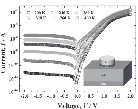
Figure 1 shows the forward and reverse bias semi-logarithmic I-V characteristics of the Au/PEDOT:PSS/n-Si SBDs in the temperature range of 200 to 400 K in 40 K steps. Sixteen Au/PEDOT:PSS/n-Si SBDs were fabricated and characterized. All diodes exhibited similar electrical charac-teristics. Furthermore, theI-Vcharacteristics of the fabricated devices was almost identical to that of Au/PEDOT:PSS/n-Si SBDs with the electrode size of 0.5-mm diameter (not shown here), implying that an electrode size dependence of electrical properties of Au/PEDOT:PSS/n-Si SBDs was insignificant. In other word, it is obvious that PEDOT:PSS interlayer employed here was uniformly formed in-between Au film and Si substrate. The leakage currents of the Au/ PEDOT:PSS/n-Si SBD increases with an increase in temper-ature and was in the range from 3.89©10¹12A (at 200 K) to 2.78©10¹6A (at 400 K) at ¹1 V. As shown in Fig. 1, the diode exhibits rectifying behavior with nonlinear behavior at low voltage, and the current of the diode increases exponentially with increasing voltage, suggesting the diode behaves like a SBD. According to thermionic emission (TE) theory, the current through a SBD at a forward bias (V²3kT/q) is given by:12)
I¼I0exp
qV nkT
1exp qVkT
; ð1Þ
whereVis the applied bias voltage,qis the electronic charge, kis the Boltzmann constant,Tis the absolute temperature in Kelvin,nis the ideality factor, andI0is the saturation current
derived from the straight-line intercept of ln(I)-Vat zero bias defined by:
I0¼AAT2exp qkTB
; ð2Þ
whereAis the contact area,A**is the effective Richardson constant of 120 A cm¹2K¹2 for n-type Si,13) and )B is the
zero bias barrier height. OnceI0is determined, the Schottky
barrier height)B(I-V) can be evaluated using the following equation:
BðIVÞ ¼kTq ln AA T2
kT
; ð3Þ
n is introduced for consideration of the deviation of the experimental I-V data from the ideal TE theory and it was obtained from the slope of the linear region of the forward bias ln(I)-Vplot and can be written from eq. (1) as:
n¼kTq dV
dðlnIÞ
; ð4Þ
The experimental values of)Bandnwere determined from the intercepts and slopes of the forward bias lnIversusVplot at each temperature using TE theory. The experimental values of )B(I-V) and n for the Au/PEDOT:PSS/n-Si SBD were 0.63 eV and 2.75 at 200 K to 0.97 eV and 1.49 at 400 K, respectively. Figure 2 shows the temperature-dependence of the zero-bias barrier height (BH) and ideality factor n. As shown in Fig. 2, the n decreases and the zero bias BH increases with increasing temperature. Such n behavior can be attributed to the existence of PEDOT:PSS interlayer, particular distribution of Nss and interface states between a
metal and semiconductor. Since the current transport across the contact interface is a temperature activated process, electrons at low temperature are able to overcome the lower barriers and therefore, the current transport will be dominated by the current flowing through the patches of low BHs,
[image:2.595.313.544.62.244.2]leading to a largern. However, as the temperature increases, more electrons have sufficient energy to overcome the BH. An apparent increase in thenand a decrease in the BH at low temperatures are possibly caused by other effects such as thickness inhomogeneities and non-uniformity of the inter-facial charges.
Furthermore, the Au/PEDOT:PSS/n-Si SBD shows a non-idealI-Vbehavior with a large ideality factor, which may be due to the presence of the PEDOT:PSS interlayer. There are various parameters that cause deviations in ideal behavior including RS and the presence of an interfacial layer.14)
Therefore,RSof the Au/PEDOT:PSS/n-Si SBD is extracted
using a method developed by Cheung and Cheun14) at a
higher current range. The calculated Rs from the plot of
dV/d(lnI) versusI (not shown) were 114.1³ at 200 K and 24³ at 400 K for the Au/PEDOT:PSS/n-Si SBD. The RS
estimated from the plot of H (I) versus I was 145³at 200 K and 32.1³ at 400 K. The Rscalculated from the dV/d(lnI)
versusIplot are in good agreement with those estimated from theH(I) versusIplot, implying their consistency and validity. Experimental results reveal thatRsincreases with decreasing
temperature. The increase of RS with a decrease in
temper-ature was due to factors responsible for an increase innand the lack of free carriers at low temperatures.
Conventional TE theory is typically used to determine the BH. Alternatively, there have been several reports deviating from this classical TE theory. The Richardson plot is drawn to obtain the BH in another way. Equation (2) can be rewritten as:
ln TI02 ¼lnðAAÞ qkTbo; ð5Þ
The conventional Richardson plot of ln(Io/T2) versus 103/T
is shown in Fig. 3. The temperature dependence of the experimental ln(Io/T2) versus 103/T plot produces a straight
line. The activation energy and Richardson constant were obtained from the slope and intercept of this straight line as 0.27 eV and 1.98©10¹7A/cm2K2, respectively. The exper-imentally-obtained Richardson constant value was much less than the theoretical Richardson constant value for n-Si. Such a large discrepancy between the experimental and theoretical values of the Richardson constant could be attributed to the calculation using the temperature-dependent I-V character-istics, which may be affected by the lateral inhomogeneity of
the BH and potential fluctuations due to the PEDOT:PSS interlayer.
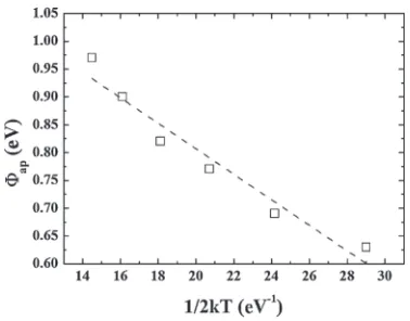
In order to explain the abnormal deviations of the I-V characteristics of the SBD from classical TE theory, the lateral distribution of BH was adopted with a Gaussian distribution. The Gaussian distribution of the BH with a mean value Schottky barrier height (bo) and a standard deviation (·o) yields the following expression for the BH:15)
ap¼boðT ¼0Þ q· 2 0
2kT; ð6Þ
where)apis the apparent Schottky barrier height and·0is the
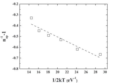
standard deviation of the )B distribution that is typically sufficiently small to be neglected. The observed variation ofn with temperature in the model is given by:15)
1
nap
1
¼μ2qμ3
2kT ; ð7Þ
where nap is the apparent ideality factor,μ2 and μ3quantify
the voltage deformation of the barrier height distribution, which may depend on temperature. Gaussian distribution may cause the decrease of zero bias BH and the influence is determined by the standard deviation. As shown in Fig. 4,
bo and·0, which correspond to the y-axis intercept and the
slope of the linear fit to the plots of )ap as a function of 1/2kT, were estimated as 1.26 eV and 0.15 eV, respectively.·0
is a general measure of the homogeneity of the Schottky barrier, with a lower ·0 value corresponding to a more
Fig. 2 Temperature dependence of)Bandnobtained from forward bias
I-Vcharacteristics for Au/PEDOT:PSS/n-Si in the range of 200400 K.
Fig. 3 Richardson plots of the In (I0/T2) versus 1000/T for the Au/
PEDOT:PSS/n-Si SBD in the range of 200400 K.
Fig. 4 The zero bias barrier height ()ap) versus 1/2kTcurves of the Au/
[image:3.595.333.520.62.208.2] [image:3.595.62.274.63.205.2] [image:3.595.333.522.257.405.2]homogeneous BH. Nevertheless, this inhomogeneity and potentialfluctuation dramatically affects the low temperature I-V characteristics. As compared to boðT¼0Þ ¼1:26eV, the ·0=0.15 eV is not small, implying Schottky barrier
[image:4.595.76.271.67.210.2]inhomogeneity in the studied SBD. As previously shown,15) barrier inhomogeneities can occur as a result of inhomoge-neities in the composition of the interfacial layer, non-uniformity of interfacial charges and interfacial layer thick-ness. Therefore, low temperature I-V characteristics are affected by this inhomogeneity and potentialfluctuation.
Figure 5 shows the plot of (n¹1¹1) versus 1/2kTfor the
Au/PEDOT:PSS/n-Si SBD. According to eq. (7), this plot should be a straight line that produces the voltage coefficients μ2 and μ3 from the intercept and slope, respectively. Values μ2=¹0.0757 V andμ3=¹0.0214 V were obtained from the
experimental data. The linear behavior of the plot shows that the ideality factornexpresses the voltage deformation of the Gaussian distribution of the SBD. If the value of μ2 is
negative, the BH should decrease with increasing forward bias, which is opposite to image force lowering. The value of μ3 is indeed negative and thus, the BH increases with
increasing forward bias. This bias dependence of BH in the distribution through mean BH and standard deviations leads to the temperature dependent ideality factor n in inhomoge-neous SBDs.16)
The conventional Richardson plot based on the thermionic emission current mechanism exhibits nonlinearity at low temperatures. Considering eqs. (2) and (6), an expression for the modified Richardson plot according to the Gaussian distribution of the BHs can be written as
ln TI02 q 2·2
0 2k2T2
¼lnðAAÞ qbokTðT ¼0Þ; ð8Þ
According to eq. (8), the modified Richardson plot of ln(I0/
T2)¹(q·)2/2(kT)2 versus 1000/Tshould be a straight line from which the slope yields the meanbo and the intercept (lnAA**) at the ordinate determiningA**for a given diode area A. As shown in Fig. 6, the modified Richardson plot has quite good linearity over the whole temperature range corresponding to a single activation energy aroundbo. From this plot, the mean bo is 1.27 eV, which is in good agreement with the mean bo (1.26 eV) extracted from the plot of )ap versus 1/2kTas shown Fig. 4. The intercept at the ordinate of the modified ln(I0/T2)¹(q·)2/2(kT)2versus
1000/T plot produces a Richardson constant A** as 134 A K¹2cm¹2 without using the temperature coefficient of the BHs. The obtained Richardson constant value is close to the theoretical value of 120 A K¹2cm¹2for n-Si.
The experimental reverse-bias C-V characteristics of the Au/PEDOT:PSS/n-Si SBD over the temperature range 200 400 K are shown in Fig. 7. C-V measurements were performed at a frequency of 1 MHz. In Schottky diodes, the depletion layer capacitance is expressed as:17)
C2 ¼ 2 ¾sNdA2
Vbi
kT q V
; ð9Þ
where Vbi is the built-in voltage, Nd is the donor
concen-tration, A is the area of the Schottky contact, and¾s is the
dielectric constant of semiconductor ¾s=11.9¾0 for n-Si,18)
and ¾0is the permittivity in a vacuum. The built-in voltage
(Vbi) is determined by extrapolating the fitted line of the
plotted C-V, while NDwas calculated from the slope of the fitted line using the following equation:19)
ND¼q2¾ s
1 dð1=C2Þ=dV
; ð10Þ
The barrier height )B(C-V) can be determined by the following equation.:
BðCVÞ ¼Vbiþ
kT q ln
NC
ND
; ð11Þ
Fig. 5 The ideality factor (nap) versus 1/2kTcurves of the Au/PEDOT:PSS
SBD according to the Gaussian distribution of barrier height.
Fig. 6 Modified Richardson ln(I0/T2)¹(q·0)2/2(kT)2(A/K2) versus 1000/
Tfor the Au/PEDOT:PSS/n-Si SBD.
Fig. 7 The reverse biasC¹2-Vcharacteristics of the Au/PEDOT:PSS/n-Si
[image:4.595.331.521.67.207.2] [image:4.595.318.536.258.415.2]withNC¼2ð2m kTÞ3=2
h3 ; ð12Þ whereNDis the donor concentration andNCis the effective
density of states in the Si conduction band edge, m*= 1.08m0is the effective mass of electrons in Si andm0is the
rest mass of the electron.20)TheNDand)B(C-V) for the Au/
[image:5.595.311.541.67.245.2]PEDOT:PSS/n-Si SBD can be calculated from eq. (10) and eq. (11), respectively. The values of )B(C-V) are given in Table 1. The barrier height values obtained from the reverse bias C¹2-V characteristics varied from 0.85 eV at 200 K to 0.69 eV at 400 K, illustrating )B(C-V) increases with decreasing temperature. The calculated values of NDvaried
from 1.32©1015cm¹3 at 200 K to 1.41©1015cm¹3 at
400 K. As shown in Table 1, the donor concentration of the n-Si slightly increases as the temperature increases. At low temperatures, mostly all of the impurities were frozen out, causing a strong increase in theRSof the diode, which makes
the measured capacitance appear smaller. More electrons may be frozen at the donor level in the freeze-out region and conduction mechanisms in the freeze-out regions are complex. Since the donor concentration increases, then the capacitance also increases with increasing temperature.
Additionally, the barrier heights obtained from C-V measurements were greater than those obtained from I-V measurements. The discrepancy between )B(C-V) and
)B(I-V) can be attributed to the characteristic nature of the C-VandI-Vmeasurement techniques, and the existence of an interfacial dipole layer or trap states at the PEDOT:PSS/n-Si interface. Additionally, the discrepancy between)B(C-V) and
)B(I-V) can be explained by the excess capacitance and SBH inhomogeneities.21) The current in the I-V measurement is
dominated by the current thatflows through the region of low SBH. Thus, the measured )B(I-V) is significantly less than the weighed arithmetic average of the SBHs. Alternatively, the barrier height determined from the C-Vorflat band was influenced by the distribution of charge at the depletion region boundary, which follows the weighted arithmetic average of the SBHs. Consequently, the SBH calculated from the zero-bias intercept assuming TE as a current transport mechanism is well below theC-Vorflat-band measured BH and the weighted arithmetic average of SBHs. Furthermore, the capacitanceCis insensitive to potentialfluctuations on a length scale less than the space charge region and the C-V measurement probes the average junction capacitance at the
interface, thereby yielding an average value for the barrier height distribution, while the I-V measurement produces a minimum value for the barrier height.22)
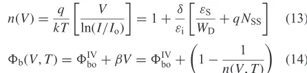
The NSS for the Au/PEDOT:PSS/n-Si SBD can be
obtained from the forward bias I-V data by taking the voltage-dependent ideality factor nðV; TÞ with the effective barrier height bðV; TÞ. The parameters of nðV; TÞ and )b (V,T) can be estimated from the following equations:23)
nðVÞ ¼kTq V
lnðI=IoÞ
¼1þ¾¤ i
¾S
WD
þqNSS
ð13Þ
bðV; TÞ ¼IVboþ¢V ¼IVboþ 1 1
nðV; TÞ
ð14Þ
whereWDis the space charge region width,¤is the thickness
of the interfacial organic layer,¾iand¾Sare the permitivities of the interfacial layer and semiconductor, and ¢(=d)eff/ dV=1¹1/n(V)) is the change in effective BH with bias voltage. As proposed by Card and Rhoderick,23)in interface states in equilibrium with the semiconductor, the ideality factor becomes greater than unity and theNSSis given by:
NSSðVÞ ¼1q ¾¤iðnðV; TÞ 1Þ W¾S D
: ð15Þ
Additionally, in n-type semiconductors, the energy interface states with respect to the conduction band edge (EC-ESS) are
obtained as:
ECESS¼qðeVÞ: ð16Þ The voltage dependence of n (V), andWDare substituted into
eq. (13) to calculate the values of NSSas a function of (EC
-ESS). Figure 8 shows the plot ofNSSas a function of (EC-ESS)
for Au/PEDOT:PSS/n-Si SBDs. The NSS value of Au/
PEDOT:PSS/n-Si SBDs decreases with increasing EC-ESS
values as a function of temperature. Additionally, theNSShas
exponential growth from the mid gap of Si toward to the bottom of the conduction band edge for all temperatures. Such behavior of NSS is a result of molecular restructuring
and reordering of PEDOT:PSS and Si molecules at the metal/ semiconductor interface under the influence of temper-ature.24) The N
SS is in the range of 1.78©1013eV¹1cm¹2
[image:5.595.47.291.105.231.2]at 200 K to 4.8©1012eV¹1cm¹2at 400 K. These values are
Table 1 Temperature-dependent values of various parameters determined fromI-VandC-Vcharacteristics of the Au/PEDOT:PSS/n-Si Schottky barrier diode.
Temperature,
T/K
Current,
Io/A
n )B
(I-V)
/eV
)B
(C-V)
/eV
ND/cm¹3
RS/³
dV/d (lnI) H(I) 200 8.38©10¹12 2.75 0.63 0.87 1.32©1015 114.1 145.3
240 1.23©10¹10 2.62 0.69 0.83 1.34©1015 100.4 77.3
280 1.13©10¹9 2.13 0.77 0.78 1.35©1015 82.2 47.3
320 1.19©10¹8 1.96 0.82 0.69 1.36©1015 46.8 38.8
360 3.05©10¹8 1.81 0.90 0.64 1.37©1015 27.1 34.2
400 7.05©10¹8 1.49 0.97 0.63 1.41©1015 24.9 32.1
Fig. 8 A plot ofNSSversusEc-Essfor the Au/PEDOT:PSS/n-Si SBD with
[image:5.595.325.548.395.448.2]similar to the results reported in the literature.25,26) The
interface states and interfacial layer between the metal and semiconductor play a significant role in the determination of the Schottky barrier parameters of the devices.
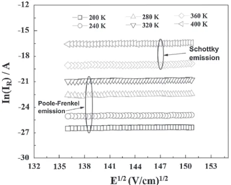
The current transport mechanism dominating the reverse leakage current in the Au/PEDOT:PSS/n-Si SBD was then investigated using the electric field dependence by consid-ering Poole-Frenkel emission and Schottky emission across the junction. The I-Vexpression for the Poole-Frenkel effect are given as:27,28)
IR¼Ioexp k¢PF BT
ffiffiffiffi E p
; ð17Þ
and for the Schottky effect,
IR¼AAT2exp ¢S kBT
ffiffiffiffi E p
ð18Þ
where ¢PFand¢Sare the Poole-Frenkel and Schottky fi
eld-lowering coefficients, respectively. The theoretical values for ¢PFand¢Sare given by:
2¢S¼¢PF¼
q3 ³¾
1=2
: ð19Þ
The Poole-Frenkel and Schottky effects can typically be distinguished by values of the field-lowering coefficients. The theoretical values of the Poole-Frenkel field-lowering coefficient (¢PF) and Schottkyfield-lowering coefficient (¢S)
for the Au/PEDOT:PSS/n-Si SBD were¢PF=2.22©10¹5
eV/m1/2V¹1/2and¢
S=1.11©10¹5eV/m1/2V¹1/2. The¢PF
value is always twice the value of¢S. Figure 9 shows the plot
of ln(IR) versus E1/2 for Au/PEDOT:PSS/n-Si SBDs at
different temperatures. The slopes determined from thefit to the data are 2.58©10¹5, 2.44©10¹5, 2.39©10¹5, 2.28©
10¹5, 1.25©10¹5 and 1.24©10¹5eV/m1/2V¹1/2 for 200,
240, 280, 320, 360, and 400 K respectively. By comparing the experimental and theoretical slopes of Au/PEDOT:PSS/ n-Si SBDs, the experimental slope determined in the low temperature region (T<320) was closer to the Poole-Frenkel
field-lowering coefficient (¢PF), whereas the experimental
slopes in the higher temperature region (T>320) was closer to the Schottkyfield-lowering coefficient (¢S). This indicates
that Poole-Frenkel emission is dominant in the lower temperature region while Schottky emission is dominant in the higher temperature region. Therefore, the current conduction mechanism of Au/PEDOT:PSS/n-Si SBDs changed from Poole-Frenkel emission to Schottky emission in the temperature range of 320360 K.
4. Conclusions
The Au/PEDOT:PSS/n-Si SBDs were fabricated by simple spin-coating technique and sequential RIE process. The influence of a thin PEDOT:PSS interlayer on the electrical properties of Au/n-type Si SBDs were studied in the temperature range of 200400 K by I-V and C-V measurements. The values of )B(I-V), )B(C-V), n and Rs
of Au/PEDOT:PSS/n-Si SBDs were estimated and illus-trated to be strongly temperature dependent. The investiga-tion results revealed an abnormal decrease in the zero-bias BH and an increase in the ideality factor n with decreasing
temperature. Additionally, the electrical properties confirmed that the temperature-dependent I-V characteristics of Au/ PEDOT:PSS/n-Si SBDs can be explained on the basis of TE theory with a Gaussian distribution of BHs. The Gaussian distribution has a mean BH bo of 1.26 eV and a standard deviation (·o) of 0.15 eV. The extracted values ofboand·o
clearly indicates the presence of Schottky barrier inhomoge-neities in the present device. A modified lnðI0=T2Þ
ðq2·2
0=2k2T2Þversus 1000/T plot producesbo andA** as 1.27 eV and 134 A/cm2K2. The obtained A** value is in
close agreement with the known value of 120 A/cm2K2 for
n-Si. The energy distribution profile ofNSSis obtained from
the forward bias I-V characteristics by considering the bias dependence of the effective BH (¯e) and ideality factor (n(V)), and the NSS values decreases with an increase in
temperature (from 1.78©1013eV¹1cm¹2 at 200 K to 4.8© 1012eV¹1cm¹2 at 400 K). Additionally, the experimental results showed that the Poole-Frenkel emission is the dominant mechanism in the reverse leakage current at low temperatures (200320 K), whereas Schottky emission is the dominant mechanism at high temperatures (360400 K).
Acknowledgements
This research was supported by Basic Research Laboratory Program (2011-0027956) through the National Research Foundation of Korea funded by the Ministry of Education, Science and Technology, and by the Converging Research Center Program (2014M3C1A8048834) through the Ministry of Science, ICT & Future Planning, Republic of Korea. It was also supported by the R&D Program (Grant No. 10045216) for Industrial Core Technology funded by the Ministry of Trade, Industry and Energy (MOTIE), Republic of Korea.
REFERENCES
1) S. Demirezen, Z. Sönmez, U. Aydemir and S. Alrindal:Curr. Appl. Phys.12(2012) 266272.
2) K. Akkılıç, M. E. Aydın, I. Uzun and T. Kılıçoglu:Synth. Met.156
(2006) 958962.
Fig. 9 Reverse current (in logarithmic scale) versusE1/2plots for the Au/
[image:6.595.312.543.70.255.2]3) N.Şimşir, H.Şafak, Ö. F. Yüksel and M. Kuş:Curr. Appl. Phys.12
(2012) 15101514.
4) K. S. Kang, K. J. Han and J. Kim:IEEE Trans. Nanotechn.8(2009) 627630.
5) W. Feng, Y. Li, J. Wu, H. Noda, A. Fujii, M. Ozaki and K. Yoshino:
J. Phys. Condens. Mater.19(2007) 186220.
6) Z. Tang, Q. Liu, I. Khatri, R. Ishikawa, K. Ueno and H. Shirai:Phys. Status Solidi C9(2012) 20752078.
7) Y. Lin and Y. Su:J. Appl. Phys.111(2012) 073712.
8) Y. Lin, B. Huang, Y. Lien, C. Lee, C. Tsai and H. Chang:J. Phys. D: Appl. Phys.42(2009) 165104.
9) M. Price, J. Foley, R. May and S. Maldonado:Appl. Phys. Lett.97
(2010) 083503.
10) J. Lin, J. Zeng, Y. Su and Y. Lin:Appl. Phys. Lett.100(2012) 153509.
11) T. Tunç, I. Dökme,Ş. Altindal and I. Uslu: Optoelectron. Adv. Mater. Rapid Commun.4(2010) 947950.
12) V. Janardhanam, H.-K. Lee, K.-H. Shim, H.-B. Hong, S.-H. Lee, K.-S. Ahn and C.-J. Choi:J. Alloy. Compd.504(2010) 146150.
13) E. H. Rhoderick and R. H. Williams:Metal-Semiconductor Contacts
2nd ed., (Clarendon Press, Oxford; U.K., 1988) pp. 3841.
14) S. K. Cheung and N. W. Cheung:Appl. Phys. Lett.49(1986) 8587.
15) Y. Song, R. Van Meirhaeghe, W. Laflere and F. Cardon:Solid State
Electron.29(1986) 633638.
16) N. Yıldırım and A. Türüt:Microelectron Eng.86(2009) 22702274.
17) S. Chand and S. Bala:Appl. Surf. Sci.252(2005) 358363.
18) S. Ashok, J. M. Borrego and R. J. Gutmann:Solid-State Electron.22
(1979) 621631.
19) R. T. Tung:Phys. Rev. B45(1992) 1350913523.
20) S. Chand and J. Kumar:J. Semicond. Sci. Technol.11(1996) 1203 1208.
21) F. Yakuphanoglu and B. F. Senkel:J. Phys. Chem. C111(2007) 1840 1846.
22) Ö. Güllü, O. Baris, M. Biber and A. Türüt:Appl. Surf. Sci.254(2008) 30393044.
23) H. C. Card and E. H. Rhoderick: J. Phys. D: Appl. Phys.4(1971) 15891601.
24) B. Akkal, Z. Benamara, A. Boudissa, N. B. Bouiadjra, M. Amrani, I. Bideux and B. Gruzza:Mater. Sci. Eng. B55(1998) 162168.
25) O. Pakma, N. Serin, T. Serin and S. Altindal:Semicond. Sci. Technol.
23(2008) 105014.
26) F. Z. Pür and A. Tataroğlu:Phys. Scr.86(2012) 035802.