Ferromagnetic Shape Memory Microactuators
Manfred Kohl
1, Berthold Krevet
1, Makoto Ohtsuka
2, Daniel Brugger
*1and Yong Liu
*2 1Forschungszentrum Karlsruhe, D-76021 Karlsruhe, Germany2Tohoku University, IMRAM, Sendai 980-8577, Japan
The technologies for fabrication, micromachining and integration of Ni–Mn–Ga thin films are developed in order to create novel microactuators and sensors. These devices simultaneously make use of the electrical, thermoelastic and ferromagnetic properties of the thin films allowing a new level of multifunctionality and, as a consequence, particularly compact designs. By adjusting the Ni-content of the thin films, the martensitic and ferromagnetic transformation temperatures are tuned close to each other above 373 K, which has important consequences on the device performance such as actuation stroke and response time. This article focuses on the mechanisms, fabrication technologies as well as typical performance characteristics of Ni–Mn–Ga microvalves and microscanners. The present state-of-the-art of FSMA microactuators is highlighted.
(Received September 22, 2005; Accepted November 7, 2005; Published March 15, 2006)
Keywords: ferromagnetic shape memory alloys, nickel–manganese–gallium thin films, microactuators, finite element simulation, fabrication technologies
1. Introduction
Ferromagnetic shape memory alloys (FSMAs) are a new class of functional materials, which show, besides shape memory and pseudoelasticity, a strong influence of an external magnetic field on the physical properties of the
martensitic phase (M-phase).1) Recent research on the
Heusler FSMA Ni–Mn–Ga showed that large strains can be
generated by a magnetic field.2,3)The underlying mechanism
has been attributed to the coupling of intercorrelated
ensembles of structural and ferromagnetic domains,1)which
implies that any reorientation of magnetic domains is associated with a reorientation of structural domains and vice versa. The option to control large strains by stress and magnetic field created a considerable research interest worldwide and led to the development of novel actuators, which show large strains and short response times without the
need of contacting the specimen.4)
For micro- and nanosystem applications, FSMA thin films are of prime interest. The development of FSMA thin film devices is, however, less motivated by a possible improve-ment of response time due to the favorable scaling behavior
of the time constants.5) Instead, one main incentive is the
increase in functionality combined with a large work output. At present, thin film technology is being developed
inten-sively.6–10) In most cases, FSMA thin films have been
fabricated by magnetron sputtering and subsequent thermal annealing providing polycrystalline thin films either in
free-standing form6,8) or deposited on a substrate.7,9,10) A few
attempts have been made to fabricate highly oriented or
epitaxial thin FSMA films.11)The exploitation of FSMA thin
films for microactuators and sensors is at the very beginning. Technological challenges are related to micromachining and system integration in a state of the art microsystem environ-ment including various interfaces (mechanical, electrical, optical, etc.).
The following two paragraphs address selected aspects of fabrication technologies and present some experimental background informations. In the subsequent paragraphs, the physical properties of the fabricated FSMA thin films and the mechanism, design and performance characteristics of microvalves and microscanners will be discussed.
2. Fabrication Technologies
A thoroughly elaborated thin film process is used to
prepare Ni–Mn–Ga thin films.6,12)Ni–Mn–Ga thin films of
10mm thickness are deposited on alumina and poly-vinyl
alcohol (PVA) substrates by a radio-frequency (RF) magne-tron sputtering apparatus (Shibaura, CFS-4ES) using hot-pressed targets. The film thickness is adjusted by the sputtering time. During sputtering, the substrate temperature is kept at 323 K. The Ar gas pressure in the sputtering
chamber is below 2:510 4Pa while the Ar gas flow is
maintained at 230 mm3s 1. The RF power is adjusted
between 50 and 200 W, which affects the Ni content and thus the phase transformation temperatures of the thin
films.13)For the case of PVA substrates, free-standing films
are obtained by substrate removal. For homogenization and ordering, as-deposited thin films are annealed at 1073 K for 36 ks. After heat treatment, the films show a regular grain structure. The typical crystallite size ranges between 0.1 and
1mm.
Important technologies required for fabrication of micro-actuators are micromachining, sacrificial layer/substrate
technology, integration and interfacing technologies.5)The
process parameters of these technologies need to be compat-ible with respect to each other and to the parameters of thin film deposition, which imposes various constraints, partic-ularly in the case of monolithic integration. Therefore, many technology combinations promising novel functionality in a large range of applications cannot be realized today. Hybrid integration technologies allow more flexibility as they rely,
e.g., on a transfer bonding technique between different
wafers.5) Thus, this approach is particularly suited for the
cases of complicated geometries or dissimilar materials. For fabrication of the FSMA microactuators presented in
*1Graduate Student, IMT, Forschungszentrum Karlsruhe. Present address: Robert Bosch GmbH, Bu¨hl, Germany
*2Graduate Student, IMT, Forschungszentrum Karlsruhe. Present address: Robert Bosch GmbH, Reutlingen, Germany
this article, a combination of magnetron sputtering on removable substrates, photochemical micromachining and transfer bonding technique has been established. The fabrication process is outlined in Fig. 1. The micromachining is performed by optical lithography and wet-chemical etching on an auxiliary wafer. Then, a micromachined carrier wafer is bonded onto the auxiliary wafer. After selective removal of the sacrificial layer, freely suspended Ni–Mn–Ga microparts are formed. Finally, the composite of carrier wafer and micromachined Ni–Mn–Ga thin film is lifted off the auxiliary wafer and transfer bonded onto the target wafer. The movable Ni–Mn–Ga microparts are connected with unstructured regions via ligaments, which will be separated during dicing. This technology is also compatible to target wafers of temperature-sensitive polymers, since critical steps of thermomechanical treatment and micromachining are performed separately.
3. Experimental
Phase transformation temperatures are determined by differential scanning calorimetry and electrical resistance characteristics. In the following, the start and finish temper-atures of the martensitic phase transformation are denoted by
Ms and Mf, the corresponding temperatures of the reverse
transformation to austenite by As and Af, respectively.
Electrical resistance characteristics of Ni–Mn–Ga thin film test devices are determined by the four-point method. The experiment is performed in a thermostat, where the ambient temperature is ramped step-wise. Stationary equilibrium conditions are adjusted by keeping sufficient waiting time at each data point.
Force-deflection characteristics are measured by attaching small calibrated weights at the movable end of the test actuators. In this case, the electrical heating current is ramped step-wise with sufficient waiting time at each data point. The corresponding displacements are determined optically by a video microscope.
4. Ni–Mn–Ga Thin Films
The chemical composition of the thin films depends, besides the target composition, on the sputtering power. In particular, the actual Ni content in the thin films is about 1– 2% higher than the target composition. For the target
composition of Ni52Mn24Ga24, for instance, the actual thin
film composition deposited at 200 W is determined to
Ni53:5Mn23:8Ga22:7 by the inductive coupled plasma method.
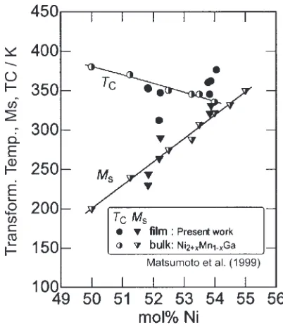
The phase transformation temperatures are determined by the chemical composition of the thin films and the heat treatment conditions. As shown in Fig. 2, a strong dependence on the Ni content is found, which is similar to bulk Ni–Mn–Ga
specimens.14) Thus, the martensitc transformation
temper-atures can be tuned particularly by the Ni content in a large range from cryogenic temperatures up to temperatures above
the Curie temperatureTC, which is much less
composition-dependent. Consequently, an optimum chemical composition can be adjusted, where the material shows ferromagnetic thermoelastic martensites at room temperature and a mixed austenitic and ferromagnetic transformation in a relatively small temperature interval. This composition is attractive for various actuator applications as will be demonstrated in the following sections.
Figure 3 shows electrical resistance characteristics of Ni– Mn–Ga thin films with two different chemical compositions of Ni53:5Mn23:8Ga22:7and Ni51:4Mn28:3Ga20:3. The martensitic
transformations are reflected by a jump-like behavior. In both cases, the transformation temperatures are well above room temperature. The hysteresis widths at the mid-points of the slopes are determined to about 6 K. The Curie temperature is reflected by a characteristic kink due to a change in electron
scattering on magnetic fluctuations atTC. For the sample with
higher Ni content, however, this behavior is not observed due to the merging of the transformation temperatures.
Fig. 1 Fabrication sequence: (1) Deposition on auxiliary wafer, (2) lithography and etching, (3) and (4) local bonding on carrier wafer and lift-off, (5) transfer bonding on target wafer.
[image:2.595.324.525.70.302.2] [image:2.595.68.269.70.248.2]For actuator applications, the stress—strain behavior of Ni–Mn–Ga thin films is of prime importance. Tensile experiments have been performed for tensile test actuators
of 10mm thickness. Figure 4 shows a typical result for a
Ni–Mn–Ga thin film with a chemical composition of
Ni53:5Mn23:8Ga22:7. Below about 30 MPa, an elastic response
is observed corresponding to a stiffness coefficient of 16 GPa. At high loads, the strain progresses quasi-plastically and reaches about 1% at 120 MPa. After unloading and subse-quent heating to austenite, a maximum recoverable strain of 0.8% is found. These results demonstrate a rather large twinning stress of about 30 MPa. Thus, the mechanical driving force to produce twinning is about an order of magnitude larger than in the case of bulk single crystalline
specimens.15)
5. Ni–Mn–Ga Microvalve
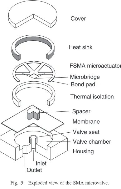
[image:3.595.69.271.72.211.2]A schematic of the Ni–Mn–Ga microvalve is shown in Fig. 5. The main components are a polymer cover, a polymer housing with an integrated valve seat, a polyimide mem-brane, a spacer and a Ni–Mn–Ga microactuator mounted in between a thermal isolation ring and a heat sink. By thermal isolation of the fluid chamber from the microactuator, parasitic heating of the housing is avoided, which has a negative impact on the valve dynamics. The microactuator
consists of a circular array of bond pads and microbridges of 2 mm length and 0.1 mm width fabricated by chemical micromachining. By thickness adjustment of the spacer, a defined prestrain is generated in the thin film. Details on the design of the microactuator and the hybrid fabrication process of the microvalve can be found in Ref. 16).
In unheated condition, a pressure difference between inlet and outlet causes a deflection of the membrane and the Ni– Mn–Ga microactuator. Thus, the valve is in a normally-open condition. By application of an electrical heating current, work is generated, which is used for the control of fluid flow and pressure difference between inlet and outlet. The maximum back pressure for closing the valve is adjusted by the spacer thickness, which prestrains the microactuator.
Figure 6 shows a time-resolved gas flow characteristic of a Ni–Mn–Ga microvalve at a pressure difference of 250 kPa. In Fig. 3 Electrical resistance characteristics of Ni–Mn–Ga thin films with
two different chemical compositions as indicated.
Fig. 4 Stress–strain characteristics determined at room temperature of a tensile test actuator of a Ni53:5Mn23:8Ga22:7thin film of 10mmthickness released from the substrate for two different maximum loads. The elastic response at small loads is indicated by a dashed line.
Membrane
Housing Spacer
FSMA microactuator
Valve seat
Valve chamber
Inlet Outlet
Thermal isolation Heat sink
Cover
Microbridge Bond pad
Fig. 5 Exploded view of the SMA microvalve.
[image:3.595.331.525.73.375.2] [image:3.595.67.271.263.403.2] [image:3.595.326.524.392.542.2]microactuator is adjusted to obtain Mf=Af temperatures of 365 K/397 K. The microvalve is operated by applying periodic heating pulses. When no extra heating power is supplied after closing the valve, a minimum opening time of about 20 ms is observed. Thus, the valve can be operated at a maximum operation frequency of 40 Hz. Compared to NiTi microvalves, the dynamic performance is improved by a factor of 3.5, which is due to the higher phase transformation temperatures. The gas flow experiments agree well with finite element simulations of the heat transfer times caused by heat
conduction and convection.17)
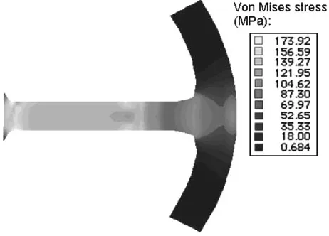
Figure 7 shows a simulated von Mises stress profile in a microbridge of Ni–Mn–Ga for 760 mW heating power applied during a time interval of 5 ms. Details of the simulation procedure are described in Ref. 18). The
deflec-tion in the center of the microbridge has been 75mm. The
corresponding profile of austenitic phase (A-phase) is shown in Fig. 8. In the region of pure A-phase an almost homoge-neous stress profile is observed. The maximum von Mises stress in this region is about 140 MPa. Close to the center of the microactuator some stress accumulation with maximum stress of 170 MPa occurs, which causes stress-induced
a sharp transition region between A- and M-phase is observed, where the stress drops abruptly. The location of the transition region depends on the stress level. In Fig. 7, for
instance, it is located at a distance of about 300mmfrom the
bond pads compared to about 200mmin the stress-free case.
By further increasing the heating power, stress-induced martensite formation can be suppressed in the center of the microactuator. In this case, however, the central region of the microactuator becomes very stiff, which is associated with a strong bending in the transition regions between A- and M-phase. Consequently, these regions show a considerable stress accumulation and buckling instability. This effect does not occur for microactuators of NiTi, since in this case the transition regions between A- and M-phase are located much closer to the bond pads due to the lower phase transformation temperatures. Therefore, von Mises stress profiles are much more homogeneous in microbridges of NiTi compared to Ni– Mn–Ga.
The microvalve application demonstrates that the choice of a particular SMA thin film has a major impact on the valve performance, which requires a specific actuator design. The use of Ni–Mn–Ga microactuators with phase transformation
temperaturesMf=Afof 365 K/397 K allows an improvement
in the dynamic performance by a factor of 3.5 compared to NiTi microactuators. However, in the case of high trans-formation temperatures, sharp martensite-austenite transition regions may occur in the freely movable microbridges, which have to be considered in the microactuator design to avoid buckling instability. The limited recovery strain of Ni–Mn– Ga thin films furthermore limits the controllable pressure difference.
6. Ni–Mn–Ga Microscanner
The function of the Ni–Mn–Ga microscanner is based on a novel actuation mechanism, which makes use of both the ferromagnetic transition and the martensitic transformation
in the material.19)As illustrated in Fig. 9, the microscanner
consists of a Ni–Mn–Ga bending actuator placed in the inhomogeneous magnetic field of a miniature permanent magnet. Depending on the temperature of the microactuator, either magnetic or shape recovery forces occur in opposite directions, while the corresponding biasing forces remain small. Thus, an almost perfect antagonism can be realized in a single component part. By applying an alternating electrical Fig. 7 Simulated von Mises stress profile in a Ni–Mn–Ga microbridge. A
heating power of 760 mW is applied during a time interval of 5 ms.
Fig. 8 Profile of A-phase corresponding to Fig. 7.
[image:4.595.53.284.375.541.2] [image:4.595.55.285.595.766.2] [image:4.595.318.535.642.736.2]current, a periodic oscillation of the beam can be excited. This motion is used to operate a scanning micromirror attached to the front end of the actuator.
The microscanner is designed as a double-beam cantilever in order to allow direct electrical heating. The lengths and widths of the cantilevers are set to 3 and 0.4 mm, respec-tively. In this case, the stoichiometry of the thin film is
Ni54:0Mn24:1Ga21:9, which results in martensitic and
auste-nitic finish temperaturesMf=Afof 388 K/438 K. The external
magnetic field is realized by a miniature permanent magnet of CoSm.
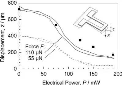
The shape recovery forces of the Ni–Mn–Ga bending actuator are determined by attaching small weights at the front end of the freely suspended double-beams. Figure 10 shows a typical displacement-power characteristic. Due to the high compliance in M-phase a large displacement is observed for small heating power. Above a critical heating power, a shape change sets in caused by the onset of the martensite-austenite phase transformation. Upon further increasing the heating power, a gradual shape change occurs due to the inhomogeneous temperature profile created by electrical heating. The minimum power to reach 90% of the maximum stroke is about 120 mW. In martensitic condition,
a maximum stroke of 600mmis obtained for a load of 110mN
applied inz-direction. For this displacement, the
correspond-ing maximum shape recovery force FSME is estimated from
the elastic response in austenitic condition to 450mN.
For calculation of the shape recovery forces, the coupling of the electrical, thermal and mechanical properties is considered by finite element simulations, which is described in Ref. 20). From the simulated evolution of stress, the
corresponding results of forcevs.displacement are calculated
as shown in Fig. 10 by squares. For a heating power between 100 and 200 mW, the simulated deflections systematically deviate from the experimental results. This result is attributed to an overestimation of the conductive cooling by the substrate, which critically depends on the thickness of the adhesive layer between bending actuator and substrate.
Oscillatory motions of the double beam are excited by applying pulsed electrical heating signals. Figure 11 shows a typical frequency characteristic of the optical scanning angle. For each frequency, the driving power is optimized while the duration of the pulse signal is kept constant between 0.7 and
2 ms to ensure a duty cycle larger than 1:6. Below a critical frequency of about 130 Hz, the scanning angle shows several maxima and minima, which strongly depend on the applied heating power. These features occur due to the phase difference between heating pulses and natural oscillations,
which depend on the heating power.21) By increasing the
driving frequency above the critical frequency, the scanning angle sharply decreases independent of the heating power. This low-pass behavior can be attributed to the dynamics of heat transfer between the double-beam and its environment. The relatively short time constants for the given dimensions are mainly due to the high phase transformation temperatures of the Ni–Mn–Ga thin films and the forced convective cooling during scanning motion. For driving frequencies above the critical frequency, the heat transfer upon cooling remains incomplete, which leads to an incomplete phase transformation. Above about 150 Hz, a broad resonance occurs reflecting the relatively strong damping in the system. The microscanner application demonstrates that the multi-functional properties of ferromagnetic shape memory thin films are very favorable for the use in microsystems. In particular, two strong antagonistic forces and corresponding small biasing forces are used here in a single beam element allowing large scanning angles in a broad range of operation frequencies. For the presented design, maximum scanning angles of 60 deg and a broad range of operation frequencies beyond 200 Hz are achieved.
7. Conclusions
The mechanisms, fabrication technologies and typical performance characteristics of Ni–Mn–Ga microvalves and microscanners are presented. The tuning of the phase transformation temperatures of off-stoichiometric Ni–Mn– Ga thin films above 373 K causes a considerable performance improvement with respect to the dynamic response. How-ever, the design of Ni–Mn–Ga microactuators requires special care to avoid sharp martensite–austenite transition regions, which may cause buckling instabilities. Further-more, the maximum recoverable strain of the investigated Ni–Mn–Ga thin films is limited to about 0.8%, which constrains the available work output.
[image:5.595.69.268.72.210.2]One particular advantage of ferromagnetic shape memory thin films in microsystems applications is the availability of Fig. 10 Experimental displacementsvs.power of the FSMA microactuator
[image:5.595.323.527.75.204.2]loaded by a force F as sketched in the inset. The squares are simulated results for the load of 110mN.
neously in a single component part. This is demonstrated for a microscanner. In this case, the intrinsic forces in Ni–Mn– Ga thin films are favorably used to generate large scanning angles in a broad range of operation frequencies, while keeping the design small and simple.
REFERENCES
1) For a recent review see,e.g., A. N. Vasil’ev, V. D. Buchel’nikov, T. Takagi, V. V. Khovailo and E. I. Estrin: Physics-Uspekhi46(2003) 559–588.
2) S. J. Murray, M. Marioni, S. M. Allen, R. C. O’Handley and T. A. Lograsso: Appl. Phys. Lett.77(2000) 886–888.
3) A. Sozinov, A. A. Likhachev, N. Lanska and K. Ullakko: Appl. Phys. Lett.80(2002) 1746–1749.
4) T. Kakeshita and K. Ullakko: MRS Bulletin27(2002) 105–109. 5) M. Kohl: Shape memory microactuators, Springer book series on
Microtechnology and MEMS, (Springer-Verlag Berlin Heidelberg, 2004).
6) M. Ohtsuka and K. Itakagi: Int. J. Appl. Electromagn. Mech.12(2000) 49–59.
7) M. Wuttig, C. Craciunescu and J. Li: Mater. Trans., JIM41(2000) 933– 37.
8) S. Isokawa, M. Suzuki, M. Ohtsuka, M. Matsumoto and K. Itagaki: Mater. Trans.42(2001) 1886–1889.
Castano, A. Labarta and X. Battle: J. Appl. Phys.91(2002) 8234–8236. 10) H. Rumpf, J. Feydt, D. Levandovski, A. Ludwig, B. Winzek, E. Quandt, P. Zhao and M. Wuttig: SPIE Proc. Series 5053 (2003) 191– 199.
11) J. W. Dong, J. Q. Xie, J. Lu, C. Adelmann, C. J. Palmstrom, J. Cui, Q. Pan, T. W. Shield, R. D. James and S. McKernan: J. Appl. Phys.95
(2004) 2593–2600.
12) M. Ohtsuka, M. Sanada, M. Matsumoto and K. Itakagi: Mater. Sci. Eng. A378(2004) 377–383.
13) M. Suzuki, M. Ohtsuka, T. Suzuki, M. Matsumoto and H. Miki: Mater. Trans., JIM40(1999) 1174–1177.
14) M. Matsumoto, T. Takagi, J. Tani, T. Kanomata, N. Muramatsu and A. N. Vasil’ev: Mater. Sci. Eng. A273–275(1999) 326–328. 15) O. Heczko, L. Straka and K. Ullakko: J. Phys. IV France112(2003)
959–962.
16) M. Kohl, D. Dittmann, E. Quandt and B. Winzek: Sensors and Actuators A83(2000) 214–219.
17) M. Kohl, Y. Liu, B. Krevet, S. Du¨rr and M. Ohtsuka: J. Phys. IV France
115(2004) 333–342.
18) M. Kohl and B. Krevet: Mater. Trans.43(2002) 1030–1036. 19) M. Kohl, D. Brugger, M. Ohtsuka and T. Takagi: Sensors and Actuators
114(2004) 445–450.
20) B. Krevet and M. Kohl: Mater. Res. Soc. Symp. Proc. Vol. 881E, (2005) CC4.10.1–6.