LEABHARLANN CHOLAISTE NA TRIONOIDE, BAILE ATHA CLIATH TRINITY COLLEGE LIBRARY DUBLIN OUscoil Atha Cliath The University of Dublin
Terms and Conditions of Use of Digitised Theses from Trinity College Library Dublin Copyright statement
All material supplied by Trinity College Library is protected by copyright (under the Copyright and Related Rights Act, 2000 as amended) and other relevant Intellectual Property Rights. By accessing and using a Digitised Thesis from Trinity College Library you acknowledge that all Intellectual Property Rights in any Works supplied are the sole and exclusive property of the copyright and/or other I PR holder. Specific copyright holders may not be explicitly identified. Use of materials from other sources within a thesis should not be construed as a claim over them.
A non-exclusive, non-transferable licence is hereby granted to those using or reproducing, in whole or in part, the material for valid purposes, providing the copyright owners are acknowledged using the normal conventions. Where specific permission to use material is required, this is identified and such permission must be sought from the copyright holder or agency cited.
Liability statement
By using a Digitised Thesis, I accept that Trinity College Dublin bears no legal responsibility for the accuracy, legality or comprehensiveness of materials contained within the thesis, and that Trinity College Dublin accepts no liability for indirect, consequential, or incidental, damages or losses arising from use of the thesis for whatever reason. Information located in a thesis may be subject to specific use constraints, details of which may not be explicitly described. It is the responsibility of potential and actual users to be aware of such constraints and to abide by them. By making use of material from a digitised thesis, you accept these copyright and disclaimer provisions. Where it is brought to the attention of Trinity College Library that there may be a breach of copyright or other restraint, it is the policy to withdraw or take down access to a thesis while the issue is being resolved.
Access Agreement
By using a Digitised Thesis from Trinity College Library you are bound by the following Terms & Conditions. Please read them carefully.
M esoscop ic T ransport in
F errom agnetic O xides
by
Jan Johannes Versluijs
A th e s is s u b m i tt e d fo r t h e d e g r e e o f D o c to r o f P h ilo s o p h y
in t h e U n iv e r s ity o f D u b lin
D e p a r t m e n t o f P h y s ic s T rin ity C o lle g e D u b lin
f^^TRlNiTY COLLEGE 1 7 DbC 2002 ^
DECLARATION
This thesis is subm itted by the undersigned for exam ination for the degree of Doctor of Philosophy at the University of Dublin. It has not been subm itted as an exercise for a degree at any other university.
This thesis, ap a rt from the advice, assistance and joint effort mentioned in the acknowl edgements and in the text, is entirely my own work.
I agree th a t the library may lend or copy this thesis freely on request.
Sum m ary
The study presented in this thesis is concerned with mesoscopic transport in half-
metallic ferromagnetic oxides. Two techniques have been developed to gain insight into the
extrinsic transport properties of these oxides.
The first, scanning tunneling potentiometry (STP), was used to correlate topographic
features of a thin film sample with the flow of cnrrent through the sample. A Scanning
Tunneling Microscope (STM) was modified succesfully to obtain simultaneously topographic
and potentiometric images of a polycrystalline (Lao.
7Sro,
3)Mn
0 3thin film. Large voltage
drops were observed to coincide with grain boundaries, whereas in the grains themselves
essentialy no change in voltage was found. Prom the voltage drop associated with the grain
boundaries, an estimate of the resistivity of these grain boundaries can be obtained. It is
found that it ranges from 3 x 10~^ 0 cm^ to 3 x 10“^
Qcm^, with an average value of 6 x 10~®
ftcm^, which is comparable with other reports in the literature.
The second method described in this thesis is the study of magneto-transport properties
in point contacts. Two tiny single crystals of either magnetite (Fe
3 0 4) or (Lao.
7Sro.
3)Mn
0 3axe mounted in a device where their separation can be controlled using a piezo-electric actu
ator. The two crystallites are brought into contact, and the resistance of the contact between
them is monitored while they are being pulled apart again. Simple vibration insulation en
sures that the contacts are stable for up to a minute or more, which is long enough to obtain
current-voltage characteristics and measure the magnetoresistance and its hysteresis.
a field. Strong non-linear current-voltage characteristics are observed, which can be fitted
to an / =
GV + cV^ law. Room temperature magnetoresistance (MR) values of up to 85
% for Fe3 0 4
and up to 45
% for (Lao,7Sro.3)Mn0 3
have been found for contacts with a low
zero-bias conductance
{G <C Go), in fields of 7 mT. For increasing conductance the MR falls
off quickly.
The huge room temperature MR values in small fields are larger than those reported
in any other ferromagnetic materials, such as ballistic Ni nanocontacts or tunnel junctions.
Here MR is defined as
. We rule out magnetostriction as the main explanation
for these large eff^ects. The magnetic hysteresis of around 1 mT shows that it is related
to the magnetization process of the crystalhtes. Two possible explanations are considered;
tunneling and spin pressure on a narrow domain wall pinned at the contact. Seeing the
contact as a magnetic tunnel junction can explain the dependence of the MR on contact
conductance, assuming that the smallest contacts, with a low conductance value, contain
fewer impurities in the insulating barrier. The bias dependence of the MR could be then be
due to magnon creation in the electrodes.
A ck n ow led gem en ts
F irst and foremost, th ank s to Mike Coey, for giving me th e o p p o rtu n ity to join his lab,
for th e interest he has shown in this work, and for th e supervision and guidance throughout.
T hanks to Fred O tt for g etting me started w ith th e S T P and point contacts set-ups, for
all th e help w ith electronics and Delphi, and for th e frequent ” ca va pas!” . Thanks to Prof
Gospodinov and Revcolevschi for providing th e Fe
3 0 4or (Lao,
7Sro,
3)M n
0 3single crystals, to
Dr SteinbeiB for giving me th e chance to work a t his group in th e In s titu t fiir Physikalische
Hochtechnologie, to Jurgen Osing, Shane M urphy and D iarm aid Mac M ath u n a for th eir help
w ith th e design and wiring of th e cryostat probes, to Dave Grouse, Jam es Egan and Mick
Reilly from th e mechanical workshop for all their help, to Joe McCauley, K en Concannon,
P a t Flanagan for all their electronical troubleshooting, and to Jackie B allentine Arm strong,
Tom Burke, Jo h n Kelly for chasing up all those orders.
T hen th ere are all the other present and former G roup D m em bers, be it long- or
short-term : Nora, Jam es, A m anda and Rhian, Rui, G areth, Treasa, Paul, Miyuki, Jiang,
Venki, M azhar, Ciara, Cora, Em m a, Oscar, Han, Guenole, Pablo, R aju, Sandrine, Virginie,
Sandrine, Sonia, Stefan, Stefan, Fernando, Eoin, K atie, Rob, Alex, Rex, Jim Cullen, Vassil
Skumryev, Sebastian, Steve, and th e numerous sum m er students. T h an k you for all your
help, th a n k you for m aking th e lab such an fun, messy, interesting, international place to
work, and for providing much entertainm ent during and outside office hours: th an k you for
all th e H am ilton coffee breaks, sessions a t th e Pav and other w atering holes, for th e theatre,
musicals, concerts, visits to th e IFC and Sinterklaas evenings, and for all th e chocolate,
baklava, turron, caipirinhas, polos, p o ta to curries and other goodies.
Table o f C ontents
S u m m a r y ... ii
A ck n o w led g em e n ts ... v
1 I n t r o d u c t io n ... 3
1.1 Spin E le c tro n ic s... 4
1.1.1 Spin p o la riz a tio n ... 6
1.1.2 Andreev Reflection ... 7
1.1.3 Spin Accumulation and D iffusion... 10
1.2 Basic Concepts of T ransport ... 11
1.2.1 Ballistic Transport and Q uantum C onductance... 12
1.2.2 Diffusive tran sp o rt and h o p p in g ... 15
1.2.3 M agnetoresistance... 16
1.3 M a te r ia ls ... 17
1.3.1 Manganese oxides ... 17
1.3.2 M a g n e tite ... 19
1.4 Scanning Tunneling P o te n tio m e try ... 22
References ... 24
2 L itera tu re R e v ie w ... 28
2.1 G rain B o u n d aries... 28
2.2 Nanowires and N a n o c o n ta c ts... 29
2.3 Domain W a lls ... 31
2.3.1 Domain Walls in nanowires and contacts ... 32
2.3.2 Domain Wall R esistivity... 35
2.3.3 Current-wall in te ra c tio n ... 41
References ... 45
3 E x p e rim en ta l S e t - u p ... 53
3.1 Sample C h ara cterisatio n ... 53
3.1.1 X-ray D iffraction... 53
3.1.2 Scanning Electron M icroscopy... 54
3.1.3 Atomic Force Microscopy and Magnetic Force M icro sc o p y ... 55
3.1.4 V ibrating Sample M ag n e to m e try ... 57
3.1.5 SQ U ID ... 59
3.1.6 Transport M easu rem en ts... 59
3.2 Scanning Tunnelling Potentiom etry ... 59
3.2.1 Set-up ... 60
3.2.2 Software ... 63
3.3.1 Room T em perature m easurem ents... 65
3.3.2 Low Tem perature M e a su re m e n ts... 69
References ... 73
4 R e s u l t s ...74
4.1 Scanning Tunnelling Potentiom etry ... 74
4.2 Point c o n ta c ts ... 78
4.2.1 (La{) 7Sro.3)M n03... 78
4.2.2 F 6304... 94
References ... I l l 5 D iscussion 8z Further W o r k ...112
5.1 Scanning Tunneling P o te n tio m e try ... 112
5.1.1 Future w o r k ... 113
5.2 Point C o n ta c t s ... 114
5.2.1 M ag n e to stric tio n ... 115
5.2.2 Transport in point c o n ta c ts ... 118
5.2.3 Spin P r e s s u re ... 128
5.2.4 Future work ... 136
References ... 139
C hapter 1
In trod u ctio n
In recent years, there have been a huge number of studies concerned with using mag
netic materials for possible applications, such as non-volatile memory devices or sensors.
This had led to a search for new materials, with higher Curie tem peratures and better in
trinsic magnetic properties. Half-metals and magnetic semiconductors especially are at the
center of the attention. But also well-known materials, such as m agnetite and Cr02, have
recaptured interest for use in novel devices. The requirements for switching devices of prac
tical use are a high Curie tem perature (> 200 °C), low power consumption, and large enough
output for small fields.
Most ferromagnetic manganese oxides exhibit a large change in electrical resistivity
when subjected to a magnetic field. This effect is most pronounced in the vicinity of the
Curie tem perature, where the Colossal Magnetoresistance is associated with a metal insulator
transition.. The potential of Colossal MagnetoResistance (CMR) for practical applications,
however, is limited because of the large field (of the order of 1 T) needed for the modification
of the intrinsic magnetic order required to observe the effect.
T he other line of investigation in this work is concerned w ith th e understanding of electronic transport in nanometric structures. This is im portant, both from a basic point of view and from a technological perspective, considering the m iniaturisation of device di m ensions in com m unication and information technology. T he study of m etallic nanowires and nanocontacts has received a great deal o f attention in the last few years. Here we ex tend this to nanocontacts in half-metallic oxides, and in particular to m agnetite, Fe3 0 4, and (Lao.7Sro.3)M n0 3 (LSMO). M agnetite is the oldest known m agnetic material; it is a ferrimagnet, w ith a high Curie tem perature (860 K). LSMO has the highest known Curie tem perature of the rnanganites (380 K). B oth have a spin polarization of RilOO %, which makes it the m ost suitable candidate for potential applications.
T his work is therefore m ainly concerned w ith the investigation o f microscopic or meso scopic scale transport properties of half-m etallic oxides, and of LSMO and m agnetite in particular. Several experim ental m ethods using point probes have been used to study trans port through grain boundaries, crystallite interfaces and nanocontacts. Section 1.1 outlines the emerging field of spin electronics, and introduces a few im portant concepts. Section 1.2 gives a basic explanation of the different transport mechanisms in th e nanometric half-m etallic oxides structures studied here. Section 1.3 introduces m agnetite and LSMO to the reader. T his chapter concludes w ith some remarks on th e Scanning Tunneling Potentiom -etry (ST P ) used here to study transport through grain boundaries in LSMO. ST P can be used to sim ultaneously measure surface topography and spatial variations of the electrical potential.
1.1
Spin E lectronics
at Bell, conventional electronics has proceeded to change modern daily life, with its use in
everyday equipment like computers, radio, television and the telephone. Electronics, with
its transistors and other devices, is based on manipulating and controlling a current flow
by applying an electric field, which acts as a force on the charge of the electrons. Only a
few devices, like relays, solenoids and Hall probes make use of a magnetic field. The fact
th at electrons have a magnetic moment (they are either spin-up or spin-down) as well as a
charge has until recently led to very little practical application: ’’Conventional electronics
has hitherto ignored the spin of the electron” [1].
Spin electronics, also known as spintronics or magnetoelectronics, is a new branch of
physics where the electron spin (as opposed to, or in addition to the electron charge) is the
active element manipulated in transport processes. This new field [2] [3] combines two well
established areas of research: magnetism and electronics. Devices based on spin electron
ics can potentially complement or replace various conventional electronic devices with an
improved performance, or even find application in quantum computing and communication
[
4].
Efforts in spin electronics are directed at a wide range of issues. Prom a fundamental
point of view, concepts such a spin-dependent transport, spin diffusion length, spin injection,
spin accumulation and spin-induced magnetic switching are receiving a great deal of atten
tion, while also the feasability of novel devices structures is studied. At the same time new
materials are investigated, with special emphasis on half-metallic m aterials and magnetic
semiconductors. All these topics are briefly introduced below.
carri-ers consisting of th e spin-up electrons and th e spin down electrons, respectively, and with
different tran sp o rt properties. For this to be a valid model, th e conduction in th e channels
has to be independent, ie. th a t there is no mixing of th e two channels. This means th a t
th e characteristic spin flip tim e has to be sufficiently long com pared w ith other scattering
processes.
1.1.1
Spin polarization
It is useful to now introduce here the concept of spin polarization. For spin electronics
to work one needs a source of spins to m anipulate. Ferrom agnetic m aterials are obvious
candidates, w ith th eir spin dependent band structure, w ith th e m ajority subband containing
electrons w ith spin parallel to th e m agnetization direction, and th e m inority subband where
th e spins are antiparallel. T he spin polarization P is a m easure of th e ratio between spin-
up and spin-down electrons ’available’ at the Fermi level. Several definitions are possible,
depending on which physical processes are being considered. Perhaps th e m ost natu ral
definition is:
p„ =
(1.1)
- I - rii
Pho to em iss io n
hv
Mag net ic
Point
T e d r o w -
A n d r e e v
1 iinnel Junction
C o n t a c t
M e s e r v e y
reflection
4
|
I
H
H
(1.2)
Figure 1.1.
Several ways to determine the spin polarization
the case of ballistic transport, the spin polarization is defined as:
^
Jt -^
{nv)^
- {mi)^
J | +
(m;)^ + (n?;)^ ’
with V the wave velocity. For diffusive transport, or tunneling through a large barrier this becom es [5]:
(1.3)
Materials with a 100 % spin polarization are known as half-metals, since only electrons with
one spin orientation are available for transport at the Fermi level.
1.1.2
A n d reev R eflection
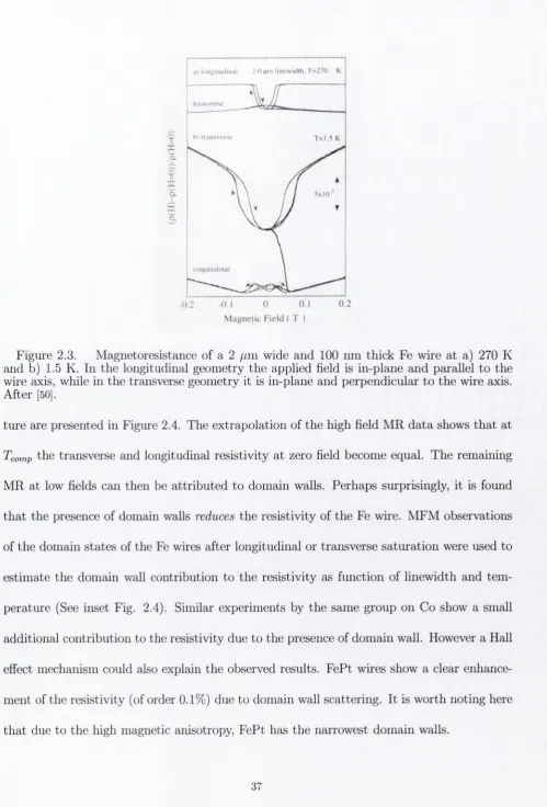
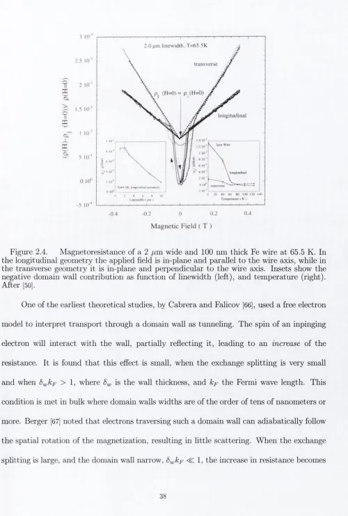
[image:16.536.13.524.30.703.2]metal is impinging on the interface. Since there are no single particle states available within
the superconducting gap A, for it to enter into the superconductor, and become part of the
supercurrent, it must be a member of a Cooper pair. This means th a t the other electron of
the pair, with spin down, leaves a hole behind at the interface. This hole, with momentum
and spin opposite to th a t of the spin-down electron, will be Andreev reflected back into the
metal, and will be part of a parallel conduction channel. This leads, for voltages less than
A /e, to a doubhng of the conductance
G = d l / d V
compared to the normal state case.
E E
in c id e n t e le c tro n
A n d re e v R e fle c te d h o le
N i ( E ) N (E )
M e ta l (P = 0 ) S u p e r c o n d u c to r
in c id e n t e le c tro n N o s ta te
a v a ila b le y
N o A n d re e v R e fle c tio n
E E
M e ta l (P = 1 0 0 % ) S u p e r c o n d u c to r
Figure 1.2.
Andreev reflection at a normal metal / superconductor interface (top) and
a t a half metal / superconductor interface (bottom).
normal metal / superconductor interface. This time, a Cooper pair cannot be formed, since
the density of states near the Fermi level in the down band is zero: there are no spin-down
electrons available. So, Andreev reflection is not possible, and the conversion from normal
current into supercurrent is blocked. This means th at in the case of a fully spin polarized
metal the conductance G = 0 for voltages smaller than A /e. So, for P = 0 the conductance
is doubled compared to the normal state conductance, because of Andreev reflection at
the interface, while for
P = 100% Andreev reflection is blocked, leading to a surpression
of the conductance. For intermediate values of the polarization, a modified version of the
Blonder-Tinkham-Klapwijk (BTK) theory [6] is needed to determine the value of P
from the
measured
d l / d V
curve. The BTK theory takes interfacial scattering into account, through
a param eter Z, with Z = 0 for ballistic transport, and Z ^ oo for tunnel junctions. For
T —> 0, y —> 0 and Z —^ 0, the theory yields:
(1.4)
where G„ is the conductance in the normal state case
(V > A), and
Pc is the contact
polarization:
''•’ft ~ (-^f) ^ F i
P r =
(1.5)
A^T [ Ef) ''-’f t + { E p ) '^’Fi ’
with
N(j the spin dependent density of states. In this case
Pc can be obtained directly from
the d l / d V
at y = 0, while for finite tem peratures and interface scattering a numerical fitting
is needed.
M a te r ia l NiFe Co Fe Ni NiMnSb LSMO CrOa
P c(% ) 37 42 45 46.5 58 78 90
Table 1. Spin polarization for different materials, after Soulen et al. [7]
variety of m aterials, see Table 1. Here a superconducting tip is driven into th e m aterial un
der investigation (or vice versa: a tip of th e m aterial is driven into a superconducting film),
and th e current-voltage characteristics m easured a t liquid helium tem peratures. T he val
ues of Pc thus obtained for th e 3d m etals are a little higher th a n those rep o rted by Tedrow
and Meservey [8], who m easured th e (tunneling) polarisation using ferrom agnetic-insulator-
superconductor junctions. However, this technique is sensitive to th e n a tu re of states in the
first few monolayers of th e ferrom agnetic electrode [9], while th e m ethod described above
probes th e polarization of th e bulk current. B oth LSMO and C r02 show a high spin po
larization, close to th e value expected for a half metallic ferrom agnet. T h e complete spin
polarization of C r02 was subsequently confirmed in A ndreev [10] and tu n n el jun ction exper
im ents [11].
1 .1 .3
S p in A c c u m u la tio n an d D iffu sio n
Assume a current flowing from a ferrom agnetic m aterial into a param agnet. The elec
trons coming from th e ferrom agnet are spin polarized, say, th ere are more spin-up electrons
th a n spin-down. So, there is a net influx into th e param agnet of spin-up electrons over
spin-down ones. This surplus is causing a certain m agnetic m om ent per volume in th e p ara
m agnetic m aterial near th e interface. At th e sam e tim e, spin flip scatterin g will tend to
flip th e up-spins into down-spins. These two com peting processes will lead to a dynamic
equilibrium , w ith a spin accum ulation near th e interface, which will drop of over a certain
length scale known as th e spin diffusion length (See Figure 1.3).T h e spin diffusion length
is strongly dependent on th e am ount of impiirities in a m aterial since these introduce more
spin-flip scattering. Typical spin diffusion lengths vary from microns in very pure m etals to
►
e ‘
Figiire 1.3.
Spin accumulation occurs when a spin-polarized current from a ferromagnet
(F) enters a paramagnet (P).
1.2
B asic C on cep ts o f Transport
the Fermi velocity
Vp =
We can now classify the two distinct transport regimes in mesoscopic structm ’es as
follows. When
X p “C L < l e , k ,the electrons are said to behave ballistically, th at is, they
travel through the structure without being scattered. The other limit,
< le,li <C
L,
is
the diffusive regime, where the electron undergo many scattering events while traversing the
structure.
1.2.1
B a llistic Transport and Q uantum C on d u ctance
The resistance of a point contact has been calculated by Sharvin [12]. It is found th at
for a small point contact, i.e. with a radius r smaller than the mean free path
Xmfp, the
resistance
R is given by
i = —
(1 6
)
R
h 47
t'
^
'
with
kp the Fermi wave vector and
A = yrr^ the area of the point contact. For a contact
with r = 10 nm this would give a resistance of 1
fl.
[19]. and electromagnetic relays [20] also show clear evidence for quantized conductance.
The quantum of conductance found is Go = ^ ~ (12.9
where e is the charge
of an electron, and
h
the Planck constant. The conductance quantization is caused by
the quantization of electron momentum in directions perpendicular to th a t of current flow.
Consider two electron gas reservoirs connected by a narrow constriction with a diameter
a,
see Fig 1.4. We assume th at the electrons move ballistically between the two reservoirs,
M-l
I
a
^2
y
Figure 1.4.
Two reservoirs with chemical potential //j and
fj
,2connected by a constriction
of size
a.
and are only scattered by the boundaries of the constriction. This means th a t the electrons
behave like a one-dimensional electron gas: in the ^-direction the electron momentum is
continuous, while in the
x-
and y-directions, due to the small size
a
of the constriction, the
momentum is quantized. The energy of the electron can then be written:
with
Ux
and
Uy
the indices for the allowed transverse modes,
h
the reduced Planck constant,
m
the electron mass, and
kz
the component of the wavevector in the
2-direction. The first
term on the right hand side of equation (1.7) is the quantized term, while the other term is
represents the continuous contribution. Applying a small potential difference between the
The number of electrons
N
then contributing to the current is:
N = ^gn{EF)i ni -
1^
2) ^
(1
-8
)with
Qn (Ep)
the density of state at the Fermi level for mode n. This leads to an expression
for the charge current
due to mode
n:
In = e V F n N = { E p ) {l^l ~ ^2) . (1-9)
with
vpn
the group velocity of mode n at the Fermi level. The density of states at the Fermi
level for a ID electron gas is given by:
‘ = j - .
(1.10)
Finally, substituting equation (1.10) into (1.9) gives a conductance
Go
per mode of:
Go = ^ = - ^ , (1.1 1 )
^ bias ^
or for the total conductance
G
;
G = N G
o= ‘^ N ,
(1.12)h
with
N
the number of available modes below the Fermi level.
When changing the size of the constriction, the number of allowed modes available
for transport changes too, and this leads to a stepwise change in the observed conductance.
W hen the size of the constriction is small enough (of the order of Angstroms), the energy
level spacing becomes larger then the thermal energy, and conductance quantization can be
observed at room temperature.
wave in each mode. In general, this condition need not hold, and this leads to the Landauer
formula, a generalization of equation (1.12)
2 N , N , \
G = -^ (
J ,
(1.13)
where the conductance is the sum over all available modes of the spin-dependent transmission
probabilities T^. For systems with spin degeneracy, and completely open or closed modes (Tj
either 0 or 1), the Landauer formula reduces to equation (1.12).
1.2.2
D iffusive tran sp ort and hopping
When an electron is scattered many times while traversing a system, it is said to behave
diffusively. Drude’s expression for the conductivity
rrof such a system,
2 7 e U e T
a = ^ =
1.14
E
m
is based on the assumption that the electrons can be viewed as an ideal gas. Here electrons
are seen as particles that can move freely in between occasional scattering events, where they
loose all information about energy, direction and velocity after each event. The electrons are
moving randomly, with the mean velocity zero. Application of an electric field will accelerate
the electrons, leading to a mean velocity, also known as the drift velocity.
1 .2 .3 M a g n e t o r e s is t a n c e
T he change in resistance of a material when applying a field is known as the magne
toresistance (MR). It is often expressed as
M R ( H ) = X 100%, (1.15)
with R { H ) and i?(0) th e resistance w ith and without applied field H. T he effects of a mag
netic field can influence th e transport properties of materials via several physical mechanisms.
The m ost well-known are normal, anistropic and giant m agnetoresistance.
Normal, or Lorentz magnetoresistance (NM R) is related to the Hall effect. Charge
carriers in a field are deflected from the direction of the current because o f th e Lorentz force
= e l f X and this reduces their effective mean free path causing a change in resistivity
of the material. To lowest order, the NM R has a dependence, w ith the largest effect
found in low resistivity m aterials, where the mean free path is long and th e electrons travel
a significant part of a cyclotron orbit before scattering (lim it UcT > 1, where lOc = e B / m ) .
Anisotropic m agnetoresistance (AMR) finds its origins in the spin-orbit coupling, which
causes th e spin-up and spin-down states to be mixed. It can be determ ined by measuring
the resistivity change as function of the angle between current direction and m agnetization.
The A M R values for m anganites and Fe3 0 4 at room tem perature are low ( ~ —0.2 %, with
a peak o f ~ —2 % at th e Curie tem perature for LCMO [22]; —0.2 % for Fe3 0 4 [23] ) .
In 1988, Baibich et al. [24] found an MR of 50 % in F e/C r multilayers, at 4.2 K. This effect was dubbed giant m agnetoresistance (GMR). It is strongly dependent on the thickness
of the layers, due to the oscillatory exchange coupling between th e ferromagnetic layers. In
of the electrons as they travel through the multilayer.
1.3
M aterials
1.3 .1
M a n g a n e se o x id e s
Mixed valence manganites,
, whereis a rare earth and
Ais a transitional metal (see Figure 1.5.), have generated a great deal of interest recently, due
Figure 1.5.
The ideal perovskite crystal structure, ABO3
. Here A is a rare eaxth (La^"*")
or transition metal (Sr^+) (black), and B is Mn^'^ or Mn'^"'', (pink). The oxygen is shown in
red.
to their peculiar magnetic and transport properties [25]. End members, like
and Ca^''‘Mn'*''‘
0 3“ are insulating and anti-ferromagnetic, while compounds with values of
X ~ 0.3 are ferromagnetic below the Curie tem perature and undergo an insulator to metal [image:26.534.18.523.36.727.2]oxygen to th e n eigh bo uring Mn^"''. D ue to th e stro n g in tra -a to m ic H u n d ’s co uphng th e
electrons can only ho p if th e spins of th e m anganese ions are p arallel. T h e configurations
M n^+—0 ^ “ —is/in '^ a n d Mn^+ —O^” —Mn^"*" are degenerate; th e lowest en erg y of th e system a t
low te m p e ra tu re corresp on ds to a parallel alignm ent. T h e tra n s fe r o f electro ns becom es m ore
difficult if th e spins of th e m anganese ions are n o t p arallel. T h is leads to a direct rela tio n
betw een co n d u ctiv ity a n d ferrom agnetism . A core of localised sp in po larised electrons form
th e t2g b an d , w hile th e co n d u ctio n b an d (th e Cg b and ) co n tain s less th e n one electro n p e r M n
ion. A m ore th o ro u g h tre a tm e n t [28] shows th a t in som e cases (like C r0 2 a n d LSM O) th e
co n d u ctio n b a n d is sp lit in to a m a jo rity an d m in ority b an d s u n til th e co n d u ctio n electrons
rem ain in only one o f th e sp in states. T hese m a terials are th e h a lf m etallic ferrom agnets.
See F ig 1.6. T h ere is som e d isp u te ab o u t w h eth er th e lower edge of th e spin-dow n b a n d in
LSM O lies ju s t above [29], or below [30] th e Ferm i level E f . However, even if it Hes below
E p , th e electrons in th e b a n d will still b e locahzed, a n d th e c u rre n t is th e n carried by th e
sp in -u p electrons. T h is is a ty p e IIIA half-m etal [31].
However, the double exchange mechanism alone is not sufficient to explain the magni
tude of the change in resistivity around
Tc
or the large resistivity for tem peratures
T > Tc
[32].
Recent work has focussed on mechanisms th a t localize the conduction electrons, such as
the Jahn-Teller effect, charge fluctuations due to cationic disorder, or magnetic impurities.
T h e usefulness of th e C M R effect for p ractical ap p licatio n s, how ever, is lim ited due
to th e large m ag n etic field req u ired to observe th e effect. However, p o ly cry stallin e sam ples
show a low field m a g n eto resista n ce w hich is ab sen t in single cry stals [33]. T h is low field M R
is therefore an ex trin sic effect; it has been re p o rte d in bulk, p o ly c ry stallin e th in films [34],
Heavy electrons
Heavy electrons
Type lA
Type IIB
Type IIIA
Figure 1.6. Schem atic bandstructure of different types o f half-m etallic ferromagnets. For T yp e lA , only spin-down electron are present at the Fermi level, the density of states for spin-up electron is zero. C r02 is an exam ple of this type half-m etal. M agnetite is an exam ple of a T ype IIB half-metallic ferromagnetic, where the carriers at the Fermi level are in a band sufficiently narrow for them to be localized. LSMO is o f type IIIA, with localized spin-up carriers and delocalized spin-down carriers. Classification after C oey et al. [31]
grain boundaries or crystallite interfaces. Compared w ith single crystals and epitaxial films
the polycrystalline sam ples have a higher resistivity, presumably caused by the presence of
grain boundaries. Tw o groups [35] [36] devised an elegant experim ent to separate the intrinsic
CMR effect from the extrinsic low field effect. W hereas the CM R effect decreases w ith lower
tem peratures, the low field MR becomes larger for decreasing tem peratures.
1.3.2
M a g n etite
M agnetite, Fe3 0 4, is the oldest m agnetic material known to man. In the form o f nat
urally m agnetized lodestone it was used as a prim itive compass by th e Chinese as far back
as lOOAD, and it has been the subject o f intensive study due to its interesting m agnetic
[image:28.535.21.523.35.382.2]as shown in Figure 1.7, with the tetrahedral sites occupied by the ferric Fe^"'' ions, and the
octahedral sites shared by ferrous Fe^+ and Fe^"*“ ions. It can be seen as a face centered
cubic lattice of oxygen anions with the iron cations situated on the interstices. The lat
tice parameter is 0.8398
A
[44].From an ionic point of view, magnetite can be written as
tively.The presence of chains of octrahedral sites along all <110> directions, leads to a low
Figure 1.7.
The magnetite (Fe3 0 4
) crystal structure. The oxygen anions (red) form a
face centered cubic lattice, with the ions cations situated on the interstices. The Fe ions
sit at either octahedral sites (green) or tetrahedral sites (brown). The chains of octrahedral
sites in the <110> directions are clearly visible.
resistivity of around 5 mOcm at room temperature, due to rapid carrier hopping between
Fe^"*" and Fe^"^ ions at these B-sites. Carriers are small polarons in a minority spin
3d^{t2g)
band
[45].All the electrons are localized, but only spin-down carriers are present at
Ep. This
is a Type
IIBhalf-metal
[31].(See Figure 1.6). The electronic configuration of the Fe^"*" ions
is 3d^, whereas that of the Fe^"*" ions is
3dP. This means that the Fe^"*" ions have one extra
electron in an anti-bonding
t2g
orbital, and it is this electron that can hop from site to site.
[image:29.535.22.524.38.522.2]respec-tetrahedral s it e s
o c ta h e d r a l s i t e s
Fe3+
Fe2+
Figure 1.8.
A schematic representation of the electronic structure of the Fe ions in
magnetite.
when the two neighbouring B-sites axe ahgned ferromagnetically which is indeed the case
for bulk magnetite, due to the dominant antiferromagnetic A-B superexchange coupling. At
a certain temperature, called the Verwey temperature,
Ty = 120 K, the resistivity increases
by about two orders of magnitude. The details of this transition are not exactly understood
[46],
but it is generally agreed that at
Ty the hopping freezes out, leading to an ordered ar
ray of Fe^"*" and Fe^"*" ions with static charges. Below the Verwey temperature the resistivity
roughly follows a T~^ law, evidence for variable range hopping
[47].Magnetite is a ferrimagnet with a Curie temperature of 850 °C. Both the Fe^'*" and
[image:30.534.14.521.29.761.2]Fe3+ ions o c c u p y te tr a h e d r a l A -site s, t h e o th e r h a lf o c c u p y h a lf o f th e o c ta h e d r a l B -site s.
Since th e s e tw o s u b la ttic e s a re co u p le d a n tife rro m a g n e tic a lly v ia s u p e re x c h a n g e , th e ir 5 fig
m o m e n ts c a n ce l o u t, a n d t h e to ta l n e t m o m e n t of ~ 4 fig p e r fo rm u la u n it F e3 0 4 com es fro m
th e Fe^"*" io n o n th e o c tr a h e d r a l B -s ite .
1.4
Scanning Tunneling P o ten tio m etry
E v e r sin ce th e first S c a n n in g T u n n e lin g M ic ro sco p e (S T M ) w as b u ild b y B in n ig et al.
[50], t h e n u m b e r o f a p p lic a tio n s h a s in c re a se d tre m e n d o u s ly . I t h a s b e e n u s e d to s tu d y th e
s tr u c tu r a l a n d e le c tro n ic p ro p e rtie s o f c o n d u c tiv e o r sem i c o n d u c tiv e su rfa c e s in a ir, liq u id
a n d U H V e n v iro n m e n ts , w ith a to m ic o r n e a r a to m ic re s o lu tio n s . S T M ’s h a v e also b e e n u se d
for lith o g ra p h y , a n d e v en for m a n ip u la tin g sin g le a to m s . S c a n n in g T u n n e lin g P o te n tio m e
t r y ( S T P ) is a n e x p e rim e n ta l te c h n iq u e t h a t e x p a n d s a S T M to s im u lta n e o u s ly im ag e th e
su rfa c e to p o g ra p h y a n d m a p th e p o te n tia l d is tr ib u tio n o f t h e m a te r ia l u n d e r s tu d y . S T P
w as first d e v e lo p e d by M u ra lt a n d P o h l [51] to s tu d y e le c tric a l t r a n s p o r t in d isc o n tin u o u s
go ld film s. S e m ic o n d u c to rs, h e te r o ju n c tio n s [52], m e ta ls [53] a n d h ig h - T c s u p e rc o n d u c to rs
[54] h av e also b e e n in v e s tig a te d , to p ro b e v a ria tio n s in t h e p o te n tia l n e a r film d isc o n tin u
itie s a n d g ra in b o u n d a rie s , a n d lo ca liz e d d efects. C o n v o lu tio n b e tw e e n t h e t ip s h a p e a n d
t h e su rfa c e to p o g ra p h y c a n le a d to a r tifa c ts in t h e p o te n tia l d is tr ib u tio n [55], b u t c a re fu l
e x p e rim e n ts h av e u n a m b ig u o u s ly sh o w n s te p s in th e p o te n tia l n e a r g ra in b o u n d a rie s a n d
c ry s ta llite in terfaces.
In th is w ork we use S T P to show t h a t t h e re s is tiv ity of p o ly c ry s ta llin e L S M O film s
com es m a in ly fro m th e g ra in b o u n d a rie s , a n d t h a t s te p s in t h e lo ca l p o te n tia l co in cid e w ith
th e s e g ra in b o u n d a rie s . S e c tio n 3.2 d eals w ith th e e x p e rim e n ta l s e t-u p , t h e e le c tro n ic s a n d
R eferences
[1] J.M.D. Coey,
Spin Electronics,
Eds M. Ziese and M. J. Thornton (Springer, Berlin
200 1).
[2] G.A. Prinz,
Science
282, 1660 (1998).
[3] J. Gregg, W. Allen, N. Viaxt, R. Kirschman, C. Sirisathitkul, J.-P. Schille, M. Gester,
S. Thompson, P. Sparks, V. Da Costa, K. Ounadjela, and M. Skvarla,
J. Magn. Magn. Mat.
175,
1 (1997).
[4] D.P. DiVincenzo,
Science
270, 255 (1995).
[5] 1.1. Mazin,
Phys. Rev. Lett.
8 3
,1427 (1999).
[6] G. E. Blonder, M. Tinkham, and T. M. Klapwijk,
Phys. Rev. B
2 5
,4515 (1982).
[7] R. J. Soulen Jr., J. M. Byers, M. S. Osofsky, B. Nadgorny, T. Ambrose, S. F. Cheng,
P. R. Broussard, C. T. Tanaka, J. Nowak, J. S. Moodera, A. Barry, and J. M. D. Coey,
Science
2 8 2
,85 (1998).
[8] P. M. Tedrow, and R. Meservey,
Phys. Rep.
23 8
,173 (1994).
[9] E. Yu. Tsymbal, and D. G. Pettifor, J.
Phys. Cond. Mat.
9
,L411 (1997).
[10] A. Anguelouch, A. Gupta, Gang Xiao, D. W. Abraham, Y. Ji, S. Ingvarsson, and C. L.
Chien.
Phys. Rev. B
6 4
,1804081 (2001).
[11] J. S. Parker, S. M. W atts, P. G. Ivanov, and P. Xiong,
Phys. Rev. Lett.
88, 196601
(2002).
[12] Yu. V. Sharvin,
Sov. Phys. JE T P
21
,655 (1965).
[13] B.J. van Wees, H. van Houten, C.W.J. Beenakker, J.G. Williamson, L.P. Kouwenhoven,
[14] J.I. Pascual, J. Mendez, J. Gomez-Herrero, A.M. Baro, N. Garcia, and Vu Thien Binh,
Phys. Rev. Lett.
7 1
,1852 (1993).
[15] J.I. Pascual, J. Mendez, J. Gomez-Herrero, A.M. Baro, N. Garcia, U. Landman, W.D.
Luedtke, E.N. Bogachek, and H.P. Cheng,
Science
2 6 7
,1793 (1995).
[16] L. Olesen, E. Laegsgaard, I. Stensgaard, F. Besenbacher, J. Schi0tz, P. Stoltze, K.W.
Jacobson, and J.K. N0rskov,
Phys. Rev. Lett.
72
,2251 (1994) 2251.
[17]
N. Agrai't, G. Rubio, and S. Vieira,
Phys. Rev. Lett.
7 4
,3995 (1995).
[18]
C.J. Muller, J.M. van Ruitenbeek, and L.J. de Jongh,
Phys. Rev. Lett.
6 9
,140 (1992).
[19]
J.L. Costa-Kramer, N. Garcia, P. Garci'a-Mochales, and P.A. Serena,
Surf. Sci.
342,
LI 144 (1995).
[20] K. Hansen, E. Laegsgaard, I. Stensgaard, and F. Besenbacher,
Phys. Rev. B
5 6
,2208
(1997).
[21] N. F. M ott,
Metal insulator transitions
(2”*^ edition) (Taylor and Francis, London,
1985).
[22]
M. Ziese, and S. P. Senna,
J. Phys.: Cond. Matt.
10
,2727 (1998).
[23]
M. Ziese, and H. J. Blythe, J.
Phys.: Cond. Matt.
12
,13 (2000).
[24] M. N. Baibich, J. M. Broto, A. Fert, F. Nguyen Van Dau, F. Petroff, P. Etienne, G.
Creuzet, A. Friedrich, and J. Ghazelas,
Phys. Rev. Lett.
6 1
,2472 (1988).
[25]
J. M. D. Coey, M. Viret, and S. von Molnar,
Adv. Phys.
48
(2), 167 (1998).
[26]
A. P. Ramirez,
J. Phys. Cond. Mat.
9
,8171 (1997).
[27]
C. Zener,
Phys. Rev.
8 1
,440 (1951).
[29]
M. Cavallini, F. Bascarini, V. Dediu, P. Nozar,
C.Taliani, and R. Zamboni,
Phys. Rev.
Lett,
submitted.
[30] B. Nadgorny, I. I. Mazin, M. Osofsky, R. J. Soulen, P. Broussard, R. M. Stroud, D. J.
Singh, V. G. Harris, A. Arsenov, and Y. Mukovskii,
Phys. Rev. B
63
,184433 (2001).
[31]
J. M. D. Coey, M. Venkatesan, and M. A. Bari,
Half-Metallic Ferromagnets
in
High
Magnetic Fields: Application in Condensed Matter Physics and Spectroscopy,
eds. C.
Berthier, L. Levy, and G. Martinez (Berlin Springer-Verlag 2002) in press.
[32]
A. J. Millis, P. B. Littlewood, and B. I. Shraiman,
Phys. Rev. Lett.
74
,5144 (1995).
[33] H. Y. Hwang, S-W. Cheong, N. P. Ong, and B. Batlogg,
Phys. Rev. Lett.
77
,2041
(1996).
[34]
A. Gupta, G. Q. Gong, G. Xiao, P. R. Duncombe, P. Lecoeur, P. Trouilloud, Y. Y.
Wang, V. P. Dravid, and J. Z. Sun,
Phys. Rev. B
54, R15629 (1996).
[35] N. D. Mathur, G. Burnell, S. P. Isaac, T. J. Jackson, B.-S. Teo, J. L. MacManus-Driscoll,
L. F. Cohen, J. E. Evetts, and M. G. Blamire,
Nature
387
,266 (1997).
[36] K. Steenbeck, T. Eick, K. Kirsch, K. O. O ’Donnell, and E. SteinbeiC,
Appl. Phys. Lett.
71
,968 (1997).
[37] J. E. Evetts, M. G. Blamire, N. D. Mathur, S. P. Isaac, B.-S. Teo, L. F. Cohen and J.
L. MacManus-Driscoll,
Phil. Trans. R. Soc. Lond. A
356
,1593 (1998).
[38] J. M. D. Coey, A. E. Berkowitz, L. Balcells, F. F. Putris, and A. Barry,
Phys. Rev.
Lett.
80
,3815 (1998).
[39] F. Guinea,
Phys. Rev. B
58
,9212 (1998).
[41] S. Lee, H. Y. Hwang, B. I. Shraiman, W. D. Ratcliff, S-W. Cheong,
Phys. Rev. Lett.
82, 4508 (1999).
[42] J. Klein, C. Hofener, S. Ulilenbruck, L. Alff, B. Buchner, and R. Gross,
Europhys. Lett.
47 (3), 371 (1999).
[43] J. Smit, and H. Wijn,
Ferrites
(Philips Technical Library, Eindhoven, 1959).
[44] V.A.M. Brabers, in Handbook of Magnetic Materials, edited by K.H.J. Buschow (North
Holland, Amsterdam, 1998), Vol 8, p. 189.
[45] M. Penicaud, B. Siberchicot, C.B. Sommers, and J. Kubler,
J. Magn. Magn. Mat.
103,
212 (1992).
[46] J.-H. Park, L.H. Tjeng, J.W. Allen, P. Metcalf, and C.T. Chen,
Phys. Rev. B
55,
12813 (1997).
[47]
N. F. Mott,
Phil Mag.
19, 835 (1969).
[48]
T. Valet, and A. Fert,
Phys. Rev. B
48, 7099 (1993).
[49]
L.I. Glazman, and K.A. Matveev,
Sov. Phys. JE T P
67, 1276 (1988).
[50]
G. Binnig, H. Rohrer, Ch. Gerber, and E. Weibel,
Phys. Rev. Lett.
49, 57 (1982).
[51]
P. Muralt, and D. W. Pohl,
Appl. Phys. Lett.
48, 514 (1986).
[52]
P. Muralt, H. Meier, D. W. Pohl, and H. W. M. Salemink,
Appl. Phys. Lett.
50, 1352
(1987).
[53] J. R. Kirtley, S. Washburn, and M. J. Brady,
Phys. Rev. Lett.
60, 1546 (1988).
[54] A. D. Kent, L Maggio-Aprile, Ph. Niedermann, Ch. Renner, and 0 . Fischer,
J. Vac.
Sci. Technol. A
8, 459 (1990).
C hapter 2
L iteratu re R ev iew
In recent years there has been a growing interest in transport on a mesoscopic scale.
On the one hand this interest is driven by the need to understand the physics of devices
with decreasing dimensions, due to the miniaturisation in the information and communica
tion technology industry. On the other hand, the advances in lithography and patterning
techniques, as well as the rise of scanning probe microscopy, has made this study of trans
port properties in mesoscopic samples possible. In this chapter we review the literature
on transport through grain boundaries (Section 2.l), and artificially made nanowires and
nanocontacts (Section 2.2). We will conclude with a brief overview of how domain walls
in small devices differ from those in bulk, the role domain walls play in transport on a
mesoscopic scale, and how they interact with charge carriers (Section 2.3).
2.1
G rain B o u n d a ries
inside the barrier. When the Fermi level of the electrode coincides with the energies of these
localized states, the conductivity is resonantly enhanced. Lattice mismatch between two
neighbouring grains will lead to dislocations and stress th a t can result in a disordered region
a few nanometers wide. It has been suggested th a t this region will have a reduced
Tc,
so
th at it may be paramagnetic [6].
2.2
N a n o w ires and N a n o c o n ta c ts
Quantization of electrical conductance has first been observed in gated structures in
two-dimensional electron gas systems [9] [10], where it is found th a t the conductance varies
in a step-like manner, with conductance values of integer multiples of Go = 2e^//i. In the
Landauer formalism the conductance G of a contact is expressed as
with
the transmission for channel
i
with spin up or down, as discussed in Section 1.2.1.
The total conductance is determined by summing over all channels. For ballistic contacts
Since the first observation of quantized conductance in 2-DEGs, the effect has also been
observed in simple metalhc nanowires such as Au, Na, P t, Ni, Bi, [11][12][13][14][15] and also in
manganites [16]. For these measurements, a wide range of experimental techniques have been
used, such as the scanning tunnelling microscope [15], mechanical break junctions [14], and
even simple table-top set-ups using macroscopic wires. Using an STM inside a transmission
electron microscope, Ohnishi
et al.
[18] were able to study the relation between conductance
and structure of gold nanocontacts. The influence of structure on the conductance of the
contact has also been recognized by Van Ruitenbeek and coworkers [19] [20], who show th at
(2.1)-th e steps in conductance are related to rearrangem ents of -th e contact.
For monovalent m etals, such as Au, th e conductance is directly related to th e num ber
of atom s in th e neck of th e contact. For m aterials w ith a higher chemical valence, for example
Al, th e relation is not so straightforw ard, as shown by Scheer et al. [21]. C urrent-voltage
characteristics of superconducting Al nanocontacts were m easured and fitted to show th a t
even for th e smallest obtainable contacts, w ith
G < Go,
th ree channels (each w ith Tj < 1)
contribute to th e tran sp o rt. For Au nanocontacts they find th a t th e sm allest contacts contain
only one channel. Similar results have been found in Nb and P b contacts [22]. O ther work, by
Garcia-M ochales
et al.
[23]has shown th a t th e shift of th e peaks in conductance histogram s,
away from integer values of Go, can be explained by th e existence of internal disorder in th e
nanocontacts.
From L andauer’s formula (2.1) it could be concluded th a t for m agnetic m aterials,
w ith th e spin degeneracy lifted, for example by applying a field, th e conductance could
vary w ith step sizes of
^Gq =
jh .
A few papers have been published, b o th theoretical
and experim ental, on this topic
[24] [25] [26].Ono
et al.
find quantization of conductance in
units of
Go
for Ni nanowires in zero field, b u t observe quantization in units of
^Go
when the
m agnetization of th e sam ple is alm ost completely satu rate d in a field of 6.7 m T. This suggest
th a t dom ain walls play a role, which is indeed confirmed by theoretical work
[25] [26].Finally,
it is w orth m entioning th a t the peaks at 0.5 Go and 1.5 Go in conductance histogram s have
even been found in non-m agnetic Au contacts under electrochem ical po ten tial control
[27].It is rem arkable experim ental fact, which seems not to be fully understood, th a t in many
nanowires and nanocontacts th e conductance does seem to be quantized a t approxim ately
2.3
D om ain Walls
In ferromagnetic materials the exchange interactions, due to Pauli’s exclusion principle,
tend to align the magnetic moments parallel to each other. In an infinite bulk sample,
the ground state would therefore be a homogeneously magnetized single domain. In finite
samples however, one single domain would lead to magnetic charges at the surface, and with
it shape demagnetizing fields. This increases the m agnetostatic energy of the system. In
order to minimize the total energy of the system, multiple domains will form, with alternating
directions of magnetization [28]. In between the domains, the magnetization vector has to
rotate from one direction to another and the resulting magnetic structure is called a domain
wall (Figures 2.1 and 2.2). Obviously, the magnetization in a domain wall is not uniform.
Figure 2.1.
A Bloch wall, where the magnetization rotates out of plane from one direc
tion to another.
Figure 2.2.
A Neel wall, where the magnetization rotates in plane from one direction to
another.
leading to an increase in exchange, anisotropy and dipole energies. The process of domain
formation is therefore a balance between the energy cost of forming the domain walls on the
one hand, and the decrease in the magnetostatic energy on the other hand. Section 2.3.1
and location of domain walls. Section 2.3.2 reviews theoretical and experimental studies on
the resistivity of a domain wall, while Section 2.3.3 finishes this chapter with a discussion of
the interactions of a domain wall with a spin and/or charge current.
2 .3 .1
D o m a in W a lls in n a n o w ires a n d c o n ta c ts
Bloch [29], followed by Landau and Lifshitz [30] was the first to study theoretically the
structure of a domain wall in the bulk. The width of the wall is determined by how quickly
the moments rotate from one direction to the other. The exchange energy, which favors
a parallel alignment of the moments, tends to broaden the wall, with only a very gradual
rotation of the magnetization vector. The anisotropy favors an abrupt change and hence a
narrow wall. The total energy
E
of the wall, is given by:
E — Epx
+
En
dV,
(2.2)with
A
the exchange stiffness,
fa
the anisotropy energy density and
9
the rotation of the
magnetization between two adjacent moments. A stable wall configuration requires a mini
mization of the total energy with respect to the rotation of magnetization:
— 0. This is
equivalent with the Euler equation for a domain wall:
^
-
2 A —
- 0
(2 3)
For the uniaxial anisotropy case, with
fa = Ku
sin^ 0, where
is the uniaxial anisotropy
constant, the wall profile can be calculated analytically:
0(z) = arctan sinh
where
6y, =
tt{ A / K
u)^is the domain wall width. Typical values for
6.^
in bulk are given in
M a te r ia l Ni Fe Co Permalloy R are earth m agnet
(nm) 72 30 15 1000 5
Table 1.Values for the domain wall w idth for a variety of m aterials, in nm.
th e above calculations, th e geo m etry of th e sam ple is assum ed to b e of no im p o rtan ce. W ith
th e increasing m in iatu rizatio n of devices an d b it size in th e m a g n etic reco rd in g ind ustry , th e
q u e stio n is if th is is still valid. B run o [32] addressed th is issue, a n d c alcu la ted th e s tru c tu re
a n d p ro p e rtie s o f a geom etrically co n strain ed d o m ain wall in a c o n stric tio n se p a ra tin g tw o
w ider regions. He found an aly tic al expressions for th e do m ain wall w id th in th re e different
m od els of constriction:
M o d el C o n str ic tio n 6 ^
C _ f So for |a;| < d gd ' 5 i > 5o for \ x \ > d ^
I I S = 5 o (l + ^ ) f
I I I S = Socosh{x/d) 2d
In th e se con striction s th e d o m ain wall w id th h as becom e in d e p e n d e n t of m a teria l p a
ra m e te rs such as th e exchange stiffness a n d an iso tro p y c o n sta n t, a n d d ep en d s only on th e
geom etry. O ne can see th a t 8^ is now of th e order of th e size of th e co n strictio n d. T hese
re su lts are confirm ed by M onte C arlo sim u latio ns of ’’isth m u s” a n d ’’h o u rg lass” geom etries
(sim ilar to M odel I a n d II, respectively) [33]. T hese sim u lation s also show th a t th e wall goes
from a Neel-like configuration for narrow constrictio ns, v ia a cross-over region to B loch-type
for larger co n strictio ns. In th e bulk, th e d om ain wall w id th 6^ is m uch larger th a n th e Ferm i
w av eleng th Xp, w hereas for n an o m etric con strictions, th e wall can becom e very narrow . T his
h a s im p o rta n t im plications for th e resistiv ity of th e do m ain w all (See S ection 2.3.2). T h e
w all energy
7^ , w hich is
2 y / A K for a bulk wall, is now for th e ’’isth m u s” g eom etry-in d e p e n d e n t of th e an isotrop y c o n stan t K .