A Thesis Submitted for the Degree of PhD at the University of Warwick
http://go.warwick.ac.uk/wrap/36261
This thesis is made available online and is protected by original copyright. Please scroll down to view the document itself.
SENSORS FOR APPLICATION IN
GAS MONITORING
by
Andrew Charles Pike
Department of Engineering
University of Warwick
A thesis submitted to the University of Warwick for the degree of Doctor of Philosophy
Heading Page
Summary vii
Acknowledgements viii
Declaration ix
List of Symbols
List of Abbreviations and Acronyms xiv
List of Chemical Symbols xvi
1 Introduction 1
1.1 Gas Monitoring Applications 1
1.2 Properties of a Gas Sensor 4
1.3 Identification of Suitable Sensor Technology 7
1.3.1 Silicon Technology 7
1.3.2 Silicon Gas Sensor Technology 8 1.3.3 Application of Silicon Micromachining 13
1.4 Research Objectives 14
1.5 Outline of Thesis 15
1.6 References 16
2 Gas Sensing Materials 19
2.1 Introduction 19
2.2 Metal Oxide Semiconductor Materials 20 2.2.1 Gas Sensing Mechanisms of Single Crystal SnO2 21 2.2.2 Thin Polycrystalline Films 25 2.2.3 Thick Polycrystalline Porous Films 25 2.2.4 Effects of Catalytic Additives 28
2.3 Organic Materials 28
2.3.1 Metal-Substituted Phthalocyanine Materials 29 2.3.2 Conducting Polymer Materials 33 2.4 Chemoresistor Design Considerations 35
2.6 References 38
3 Design of Silicon Chemoresistive Devices 42
3.1 Introduction 42
3.2 Design of Sensor Array Devices 45 3.2.1 Gold Electrode Design for Sensor Array Devices 47 3.2.2 Photoresist Layout Design 52 3.2.3 Design of Micro-Hotplate 53 3.2.4 Layout Design for Silicon Nitride 61 3.2.5 Layout Design for KOH Back-Etch 62 3.3 Design of Discrete Sensor Devices 63
3.4 Design of Bridge Devices 67
3.5 Conclusions 69
3.6 References 69
4 Fabrication Details 71
4.1 Introduction 71
4.2 Silicon Wafer Processing 71
4.2.1 Array Device Wafer Processing 72 4.2.2 Discrete and Bridge Device Processing 75
4.3 Focused Ion Beam Milling 77
4.4 Deposition of Gas-Sensitive Films 81 4.4.1 Metal-Substituted Phthalocyanine Deposition 81 4.4.2 Electrochemical Deposition of Conducting Polymers 83
4.4.3 5n02 Deposition 88
4.5 Fabrication of a Hybrid SAD 90
4.6 Conclusions 91
5 Modelling of Chemoresistive Gas Sensors 95
5.1 Introduction 95
5.2 Empirical Expressions for Steady-State Characteristics 97 5.3 Diffusion and Reaction Models 99
5.3.1 Adsorption Isotherms 100
5.3.2 Diffusion-Reaction Considerations 102 5.4 Modelling of Film Conduction 105 5.4.1 Conduction in MOS Films 106 5.4.2 Conduction in Organic Materials 108 5.5 Modelling Chemoresistor Geometry 109 5.6 Theoretical Response of an Intelligent Dual Sensor 111
5.7 Conclusions 117
5.8 References 117
6 Characterisation and Modelling of Micro-Hotplates 120
6.1 Introduction 120
6.2 Steady-State Characterisation of MHP 121 6.2.1 Characterisation of Microheater
Resistance and Temperature 121
6.2.2 Steady-State Power Consumption of Micro-Hotplates 124 6.2.3 Contributions from Different Thermal Loss Mechanisms 126 6.2.4 Assessment of Model Used to Design Micro-Hotplate 130 6.2.5 Review of the Micro-Hotplate Physical Properties that
Determine Thermal Power Loss 133 6.3 Transient Micro-Hotplate Characteristics 134 6.3.1 Measured Transient Response 135 6.3.2 Analysis of Transient Characteristics 140 6.4 Modelling of Micro-Hotplate 145
6.4.1 Analytical Modelling 146
6.4.2 Numerical Modelling 147
6.5 Conclusions 158
7 Gas Sensor Test System 161
7.1 Introduction 161
7.2 Test System Design 162
7.2.1 Gas Flow Hardware 164
7.2.2 Virtual Instrument 169
7.2.3 Design of Signal Conditioning Circuitry 170 7.2.4 Fail-Safe Leak Detection System 181
7.2.5 Test Sequence Program 181
7.3 Test System Commissioning 189
7.3.1 Steady-State System Calibration 191
7.3.2 Test System Dynamics 199
7.4 Data Analysis 202
7.5 Conclusions 202
7.6 References 203
8 Characterisation of Chemoresistors 205
8.1 Introduction 205
8.2 Characterisation of XPc Chemoresistors 206 8.3 Characterisation of Sn02 Chemoresistors 209 8.3.1 Thin Film Sn0 2 Chemoresistors 209 8.3.2 Thick Film Sn02 Chemoresistors 222 8.4 Characterisation of the Dual Sensor Device 231 8.5 Typical Characteristics for CP Chemoresistors 234
8.6 Conclusions 235
8.7 References 237
9 Conclusions 238
9.1 Research Approach to Achieve Objectives 238 9.2 Conclusions from the Characterisation of SADs 240 9.3 Proposal of an Intelligent Sensor System 241
9.5 References 248
Appendix A: Sensor Design Cells 249
Appendix B: Sensor Design Fabrication Masks 259
Summary
The growing concerns over our exposure to hazardous substances have been addressed by stringent legislation to ensure air quality. A wide variety of applications have therefore arisen which require the reliable detection of hazardous gases. Hence, the motivation behind the research presented in this thesis was the aim of developing a portable gas monitor to detect nitrogen dioxide, carbon monoxide and volatile organic compounds (e.g. benzene, toluene). The need to improve gas sensor technology for suitability to this demanding application has been identified. Thus, the objectives were to develop a number of ultra-low power devices consisting of an array of chemoresistive gas sensors for incorporation into an intelligent sensor system. The operation of these sensors relies on the measurement of a change in resistance of a gas-sensitive material when exposed to specific gases.
Silicon technology has been employed in order to obtain reproducible, miniaturised sensors with a low unit cost. Furthermore, chemoresistors employing metal oxide semiconductor (MOS), metal-substituted phthalocyanine (XPc) and conducting polymer (CP) materials have been used because of their sensitivity to the gases of interest.
Common problems associated with these materials are poor specificity to a target gas and poor stability. However, the approach to minimising these problems was to design arrays of cross-sensitive chemoresistors for use in a microprocessor-based intelligent sensor system. The microprocessor applies a pattern recognition algorithm to the sensor outputs to extract the required information. This thesis describes the design, fabrication and characterisation of these sensor arrays.
MOS and XPc materials have shown an optimum performance at elevated temperatures. Micromachining techniques have therefore been employed to integrate resistance heaters in a micro-hotplate structure, which can allow temperatures of 600°C to be attained in —15 ms with a typical power consumption of —150 mW/sensor. A pulsed mode of operation should provide average power consumptions of less than 1 mW. A low power consumption is critical for a portable battery-powered instrument. The design, modelling and characterisation of the micro-hotplate structures have also been described.
The design and development of a novel automated gas sensor test system was also fundamental to this research, in order to accurately characterise sensor responses and to validate theoretical models.
Acknowledgements
I would like to thank my academic supervisor, Dr Julian Gardner, for giving me the opportunity of studying in this field and for his guidance and tuition during my PhD. I would like to acknowledge the Health and Safety Executive (HSE) for their funding of my CASE Award. Similar gratitude is given to the Engineering and Physical Science Research Council (EPSRC) for a maintenance award.
The practical stages of my studies employed the facilities and expertise of the certain institutions. I am therefore very thankful to all the associated staff, and in particular:
Sensor Research Laboratory, Warwick University; Frank Courtney (Technician) for
his practical assistance.
Institute of Microtechnology, University of Neuchatel, Switzerland; N.F. de Rooij
(Director), M. Koudelka-Hep, and P.A. Clerc who coordinated the silicon wafer processing.
Institute of Physical and Theoretical Chemistry, University of Tiibingen, Germany;
W. GOpel (Director), A. Hierlemann, and M. Schwiezer-Berberich for the deposition of thin and thick films of Sn02.
Institute of Physics and Technology of Materials, Bucharest, Romania; N. Barsan for
deposition of thick 5n0 2 films.
Department of Chemistry, University of Southampton, UK; P.N. Bartlett (Director),
and J. Elliott for conducting polymer deposition.
HSE, Sheffield, UK; S.C. Thorpe (CASE award supervisor) for XPc deposition.
Rutherford Appleton Laboratories, Didcot, UK; J. Bryant for photolithographic mask
production, and J. Watson for FB3M processing.
Declaration
The work described in this thesis is entirely original and my own, except where otherwise indicated.
Parts of this work has been presented at international conferences:
1. Sensors and their Applications VII, 10-13 September 1995, Dublin,
Nanoengineered Dual Sensor Device for Intelligent Monitoring of Gases, A.C. Pike and J.W. Gardner.
2. Eurosensors VIII, 25-28 September 1994, Toulouse, France, Integrated Array
Sensor for Detecting Organic Solvents, J.W. Gardner and A.C. Pike et al.
Parts of the work contained in this thesis have also been published in the scientific literature:
3. J.W. Gardner, A.C. Pike, N.F. de Rooij, M. Koudelka-Hep, P.A. Clerc, A. Hierlemann and W. Giipel, Integrated Array Sensor for Detecting Organic Solvents, Sensors and Actuators B, 26-27 (1995) 135-139.
List of Symbols
Symbol Description Units
Roman letters:
a Distance across the active area In
A Area m2
A Adsorption gas species A Constant of proportionality
c P Specific heat capacity at constant pressure J IC1 kg'
C Electrical capacitance F
C Thermal capacitance J ICI
C Gas concentration 111-3
Cext External gas concentration m-3
Cx Local gas concentration at x m-2
DA Diffusion coefficient of gas species A m2S4
e Electron charge C
E Electric field V m1
F Volumetric flow-rate M. S3 -1
Fm Measured volumetric flow-rate 11.1 3 S -1
Fset Demanded volumetric flow-rate m 3 - S 1
G Electrical conductance S
G, Thermal conductance (convection) W ICI
Gr Thermal conductance (radiation) W ICI
Gcr Thermal conductance associated with convection and W IC1
radiation
Go Base-line conductance S
h Heat transfer coefficient vv K-1 m-2
H Absolute humidity mol
H(s) Laplace transfer function
i Current A
I Current A
J Current density A 111-2
Symbol Description Units kb Backward reaction rate
kf Forward reaction rate kr Reaction rate of removal
K Sensitivity coefficient
-K Arbitrary constant
1 Electrode length m
L Length of microheater m
LD Debye length m
m Membrane thickness m
111(co) Magnitude of frequency response
n Electron concentration m-3
nb Bulk concentration of electrons m-3
N Number of active sites
-NS Electronic surface charge C rri2
N, Local number of active sites
P Hole concentration m-3
Po Base-line number of electronic holes -Pa Thermal convective power loss W
PE Electrical power W
PH Electrical microheater power W
Pm Thermal conductive power loss W
Pr Thermal radiation power loss W PT Total micro-hotplate thermal power loss W
q Heat flow W ni2
q Heat generated per unit volume W rri3
3 Radius m
R Resistance 52
R1-4 Thermal resistance associated with thermal K W1
conduction through the membrane
RB Baseline resistance CI
Symbol Description Units
RH Microheater resistance S2
RS Sheet resistance S2/sq.
ARS Microheater resistance shift S2
RT Resistance at a specific temperature S2
Rth Thermal resistance K W-1
RO Base-line resistance S2
.9t Fractional change in resistance response S Gas-sensitivity coefficient
t Time s
t Metallisation thickness m
T Temperature K
T1 Temperature at point '1' K
T2 Temperature at point '2' K
Ta Ambient temperature K
TH Heater temperature K
AT Change in temperature K
u Distance across membrane m
U Flow rate m s-1
Va Voltage at node a V
vi Input voltage V
Vo Output voltage V
vss Steady-state voltage V
3 Voltage V
3 Volume m3
Vpk-pk Peak to peak voltage V
VS Electronic potential barrier eV
w Inter-electrode gap m
W Width of microheater m
x Distance through gas-sensitive film m
Xb Position of moving-boundary m
X' x/xd
Greek letters:
Temperature coefficient of resistivity K-1 Olp Thermal power loss coefficient W K-1
Coefficient relating to a power law
PP Thermal power loss coefficient W IC2
Sn Change in number of immobilised electrons Sp Change in number of holes
Effective emissivity F m-1
So Vacuum permittivity F m-1
Er Relative dielectric permittivity
-K Thermal conductivity W m-1 K-1
Bulk mean free path
lie Electron mobility m2 v-1 s-1
Hole mobility m2 V-1 S-1
0 Site occupancy
-P Electrical resistivity E2 m
Density (mass) kg 111-3
Bulk electrical resistivity m Stefan-Boltzmann constant W m-2K-4
a Electrical conductivity S m-1
Bulk electrical conductivity S m-1 Local electrical conductivity S m-1
Z Time constant
T90 Response time of signal to reach 90 % of the final s
steady-state signal
List of Abbreviations and Acronyms
Term Definition
a.c. ADC ANN ASIC BAW COSHH CP CuPc CVD DAC DAQ d.c. d.i.l. DIO DMM FEM 1-113 M HSE IC I/V LED LPCVD LUT MEL MFC MgPc MHP MOS MSB MUX Alternating Current
Analogue to Digital Converter Artificial Neural Network
Application Specific Integrated Circuit Bulk Acoustic Wave
Control Of Substances Hazardous to Health Conducting Polymer
Copper Phthalocyanine Chemical Vapour Deposition Digital to Analogue Converter Data Acquisition
Direct Current dual-in-line
Digital Input/Output Digital Multi-Meter Finite Element Method Focused Ion Beam Milling Health and Safety Executive Integrated Circuit
Current/Voltage Light Emitting Diode
Low Pressure Chemical Vapour Deposition Look-Up Table
Maximum Exposure Limit Mass Flow Controller Magnesium Phthalocyanine MicroHotplate
Metal Oxide Semiconductor Most Significant Bit
OES Occupational Exposure Standard
PAn Poly(Aniline)
PARC Pattern Recognition
PbPc Lead Phthalocyanine
PC Personal Computer
PCB Printed Circuit Board
Pk-Pk Peak to Peak
PPy Poly(Pyrrole)
PRT Platinum Resistance Thermometer PVD Physical Vapour Deposition
RAM Random Access Memory
RH Relative Humidity
ROM Read Only Memory
RT Room Temperature
SAD Sensor Array Device
SAW Surface Acoustic Wave
SCE Saturated Calomel Electrode SCS Single Crystal Silicon
TCR Temperature Coefficient of Resistance TEM Transmission Electron Microscopy TTL Transistor-Transistor Logic
UV Ultra-Violet
VI Virtual Instrument
List of Chemical Symbols
Chemical Symbol Chemical substance
Au Gold
CH4 Methane C12 Chlorine
CO2 Carbon Dioxide
CO Carbon Monoxide
F2 Florine
Ga Gallium
HC1 Hydrogen Chloride
H2 Hydrogen
H2S Hydrogen Sulfide
KOH Potassium Hydroxide
N2 Nitrogen
N20 Nitrous Oxide
NO Nitrogen Oxide
NO2 Nitrogen Dioxide NH3 Ammonia
02 Oxygen
Pd Palladium
Pt Platinum
Si Silicon
SiN. Silicon Nitride of unspecified stoichiometry
Si3N4 Silicon Nitride
Si02 Silicon Dioxide SnO2 Tin Dioxide
SixOyNz Silicon Oxynitride of unspecified stoichiometry
Ta Tantalum
Chapter 1
1. Introduction
The main aim of this Chapter is to outline the desired specification of an instrument for gas sensing. One instrument of particular interest is a portable hazardous gas monitor. The sensor technologies most suited for portable instrumentation and the enabling technologies are considered and hence, the case made for investigating silicon micromachined chemoresistive gas sensors.
The research objectives and an outline of this thesis are given at the end of this Chapter.
1.1 Gas Monitoring Applications
to detect toxic CO levels. However, this often led to a false sense of security because the sensitivity of the canary to CO was notoriously unreliable (ranging from 1,200 to
1,800 ppm). The strenuous work frequently carried out by the miner increased the rate of the poisoning by CO above that of the bird's (e.g. via increased respiration), hence the miner occasionally reached their critical level first [1.1].
The unreliability of the early techniques clearly demonstrated the need for a reliable and accurate gas monitor. Improvements made in gas-monitoring instrumentation are now capable of detecting the main hazardous gases at fixed monitoring stations, or the detection of one hazardous gas with a portable instrument. However, the occasional accident still questions the adequacy of a miner's personal protection to all hazardous gases [1.2]. Apart from the naturally occurring gases, additional hazardous gases (e.g. CO, CO 2, NO and NO2 and sulfur compounds) are emitted from the engine exhausts of mining equipment. Furthermore, non-toxic gases like CO2, N2 and H2 act as simple asphyxiants when present at high enough concentrations as to reduce the oxygen content in air by dilution. Finally, H2 and volatile organic compounds (VOCs) e.g. benzene and toluene, have been identified as products from a mine fire. Ideally, each miner should carry a portable gas monitor which could identify and warn against all of these hazards. Unfortunately, current sensor technology is not capable of meeting this demanding specification.
years that a domestic CO alarm has become generally available, because of the difficulty in employing a sensor technology that fulfils the stringent requirements at a low unit cost [1.6].
The need for gas detection equipment has stimulated the development of chemical sensors that employ a wide variety of materials and technologies [1.7]. In some cases, the inadequacies of the sensor technology have been compensated for by the simultaneous development in processing power via microelectronics. For example, microprocessor-based instruments employing an array of non-specific sensors can apply pattern recognition (PARC) software or characteristic look-up tables (LUTs) to improve the performance of the sensor system. This approach has been commercially developed into a related instrument whose operation mimics that of the human olfaction system, it is thus referred to as an electronic nose [1.8]. These instruments allow a qualitative assessment of odours in the food, drink, medical and manufacturing industries.
If a gas monitoring instrument is to be used in a potentially explosive atmosphere, then there is specific legislation that requires the instrument is intrinsically safe (British Standard BSEN 50020, BSEN 50014). The standards take into account the electronic, mechanical and operational safety considerations. The electronic standards ensure that no sparking is possible and that the maximum surface temperature exposed to the atmosphere is below that of the ignition temperature of the combustible gases.
The research reported in this thesis was supported by the Health and Safety Executive (HSE), Sheffield, who highlighted the application for a portable hazardous gas monitoring instrument to detect CO, NO 2 and VOC hazards. At this stage the VOCs of interest are limited to benzene and toluene. The exposure limits for these gases and vapours of interest are shown in Table 1.1 [1.5].
Table 1.1 Exposure limits of gases and vapours of interest. All values form the OES unless otherwise stated.
Gas/Vapour Long-term exposure limit (PPm)
Short-term exposure limit (PPIn)
NO2 3 5
CO 50 300
Benzene 5 (MEL)
-Toluene 50 150
Limiting the detection to a few gases of interest makes the objective of developing a suitable portable instrument a real possibility. Therefore, the next Section describes the general gas sensor characteristics that are essential for operation in a portable instrument, which provides the basis for assessment of a sensor's performance. In this way, the most suitable sensor technology for the application was selected, as described in Section 1.3.
1.2 Properties of a Gas Sensor
X(t)
Time
3r,
t,
Time Gas Monitoring Instrument System
Physical
Variable mo GasSensor
Signal
Modification Display(or Alarm) Informationto Operator
Figure 1.1 Block diagram of a gas monitoring instrument.
The sensor converts the physical gas concentration into an electrical signal. The electrical signal then has to be modified into a form which can be displayed to the operator, or in the case of hazardous gases, it may be used to give an early warning. The type of modifier depends on the sensor technology employed and the information required. During sensor testing, the function relating the electrical signal to a target gas concentration is termed the calibration function. This function should be of a form where it can be incorporated in the modifier block to determine accurately the target gas concentration. In general, a simple calibration function requires less signal processing, which has to be performed by the instrument. However, it has been found that many sensor calibration functions are far from ideal and require sophisticated mathematical processing.
The definitions of parameters describing sensor characteristics are now considered for the sensor system, as shown in Figure 1.2.
Measurand Sensor Output
x A y A
Gas
Sensor --o-y(t) yo 0
Figure 1.2 Gas sensor block diagram (centre), giving an example of a sensor output response (right) to
a step change in a measurand (e.g. target gas concentration).
base-line is called the response (i.e. Ay = y'-y.). The steady-state response is usually defined as a dimensionless parameter e.g. y'/y 0, or Ay/yo. The absolute sensitivity of the sensor is the ratio of the change of the output signal to the change in the measurand (dy/dx). Alternatively, the relative sensor sensitivity is the absolute sensor sensitivity normalised by the base-line output signal (i.e. dy/yo.dx). Response times are generally defined as the time to achieve a certain percentage of the final change in the sensor signal e.g. 1-90 is defined as the time to reach 90 % of the final sensor signal. If the system is first order, a time constant defines the time taken to reach 63 % of the final sensor output. The sensor signal has to be fully reversible back to the base-line when re-exposed to clean air. Ideally the sensor should have a high sensitivity, to just the one physical variable of interest (i.e. be specific) with an instantaneous response time. Unfortunately, this is not the case for practical gas sensors. It is often found that the sensor is also sensitive to other physical variables (e.g. other gases, vapours and temperature), which causes a change in the calibration curve in the presence of these interfering components. To gauge the amount of cross-sensitivity the term specificity is used. This undesirable property is caused by the sensor's absolute sensitivities to the other physical variables. If the sensitivity is large to one measurand compared with the others, then the sensor may be regarded as specific. Selectivity is defined as the ability of a sensor to respond primarily to only one species in the presence of other species. A high selectivity means that the contribution from the gas of interest dominates and that the contribution from the interfering gases is minimal. The properties of a sensor may also be unstable and drift which are characterised by a change in output while the input conditions are kept constant. This can affect the base-line sensor output, sensitivity and repeatability and in turn can make calibration of the sensor problematic.
be fast enough to allow detection well within the short-term exposure limit (e.g. r <
60 s). The long-term exposure limit determines the sensitivity requirements for the sensor. The power requirements of such an instrument should also be very low because, for portability the instrument would need to be battery-powered.
A sensor technology does not exist that can provide all of the ideal characteristics described above, as will be outlined in the following Section. However, as is mentioned earlier the performance of many sensor systems can be improved by incorporating microelectronics with more processing power.
1.3 Identification of Suitable Sensor Technology
1.3.1 Silicon Technology
The production of gas sensors has in the past employed IC fabrication technologies with either thin film and/or thick film techniques. The difference between thin and thick films is not so much in the difference of the film thickness, but more in the difference of the deposition technique.
Thick film technology is based on screen printing techniques [1.9], usually printing on alumina substrates. The benefits with this technique are a reasonably compact sensor at a low cost. Unfortunately, the limitation on the achievable miniaturisation of the device feature size and the poor dimensional control, is due to the intrinsic resolution limitation of the screen printing technique (— 20 gm). Reproducible film properties are also hard to control.
reduction and on-chip compensation. Sensors with this type of integrated circuitry are referred to as intelligent sensors [1.13]. With the costs of microprocessor and Application Specific Integrated Circuit (ASIC) technology reducing each year, it is a real possibility to have a low-cost miniature hazardous gas monitor with an improved accuracy and reliability.
The suitability of silicon technology for the design of microsensors in portable instrument applications led to its selection as the enabling technology for my research.
1.3.2 Silicon Gas Sensor Technology
There are a wide variety of silicon gas sensors that are classified according to the physical parameter which is modulated by the interaction with the target gas. Using the convention employed by GOpel et al. [1.14] the classes of solid-state gas sensors are: electrochemical, electronic conductance and capacitance, field effect, calorimetric, mass-sensitive and optical. The initial criteria to choose a sensor technology for investigation was to ensure it could employ silicon technology and enable sensors which have a suitable performance for the detection of the gases of interest (e.g. CO, NO 2 and VOCs). Using these requirements, the class of gas sensors based on measuring electronic resistance (or conductance) were highlighted as the most suitable, as explained later in greater detail. However, the reasons for rejecting the other sensor technologies are summarised in Table 1.2, for further details on these sensors see [1.14] and the references cited therein.
The exposure of an electronic conductance sensor to a gas of interest causes a change in electrical resistance of a sensing element. Thus, they are commonly referred to as chemoresistors, which is the convention used throughout this thesis. Chemoresistors have employed a wide variety of materials which have showed sensitivity to an even wider range of gases and vapours including CO, NO2, and VOCs. The survey by GOpel et al. [1.14] shows that metal-oxide semiconductors (MOS), in particular tin oxide (Sn0 2) have the greatest sensitivity to CO, while the most NO2-sensitive materials are metal-substituted phthalocyanines (XPc). More recently it has been reported by Miasik et al. [1.15] that conducting polymer (CP) materials are sensitive to a wide range of gases and vapours. Furthermore, Bartlett et
al. [1.16] have demonstrated that CPs are sensitive to methanol and other organic
Table 1.2 Basis for judging sensor technologies unsuitable for the application specified in Section 1.1.
Gas Sensor Class Unsuitable Features
Electrochemical The number of gases showing sensitivity to this class of sensor is limited by the different types of solid electrolyte employed. Thin film processing techniques have made this technology suitable for portable instrument applications, albeit, limited to 0 2 and H2.
Field Effect Apart from a slow response time and poor stability, the sensitivity has been limited to H2, H2S, NH3 , CO and larger hydrogen-containing molecules e.g. alcohols, acetylene and ethylene.
Electronic Capacitance
Sensors employing changes in the dielectric constant have only been commercially successful in determining the water partial pressure in air, i.e. humidity.
Calorimetric This sensor type are in general limited to the detection of combustible gases e.g. H2, CO and small hydrocarbon molecules. The most technologically mature type of calorimetric sensor is the Pellistor', which is prone to long-term drift effects caused by poisoning.
Mass-sensitive l- The operation of these devices employs a piezoelectric substrate e.g. quartz. Integration of SAW technology on silicon requires a more complex fabrication process.
Optical The integration of optical technology with silicon technology is not appropriate for a portable instrument, because of complexity, size restraints and at present costs.
Gas-Sensitive Material
Electrical Connection Electrodes
Electrical Insulator
— Silicon Substrate
fel
Measuring changes in resistance has the advantage of requiring a more straightforward interface circuitry, which would be beneficial for producing a small, low-power portable instrument.
The gas-sensitive properties of MOS, XPc and CP materials coupled with their ability to be deposited in planar films makes them highly suited to silicon planar technology. Using thin film processing techniques allows a higher degree of control over the sensor structure and therefore increases reproducibility. The typical structure of a planar chemoresistor is shown Figure 1.3 that employs a constant voltage circuit.
Figure 1.3 General structure of a chemoresistive gas sensor with a constant voltage supply (\Tref).
An electrical insulator, e.g. silicon dioxide (Si02) or silicon nitride (Si 3N4) is deposited over the silicon substrate to form a suitable substrate onto which the gas-sensitive material is deposited. The resistance may be determined from the d.c. current/voltage (UV) characteristics measured across the electrodes. Both MOS and XPc materials are known to have an optimal performance at a specific temperature. The optimum operating temperature for MOS film can range between approximately 200°C to 600°C, while XPc films operate between approximately 150°C to 200°C. Microheaters can be integrated into the sensor designs by using thin film processes and hence provide temperature control of the gas-sensitive material.
C„ Temperature
Humidity
Resistance
performance [1.17]. However, material improvements have not totally alleviated the problems of poor specificity or long-term drift. In the mid 1980s Zaromb and Stetter [1.18] proposed a different approach to improve the selectivity of several sensor systems, which employed an array of cross-sensitive sensors in conjunction with a microprocessor. In which the microprocessor applies a pattern recognition (PARC) algorithm to the sensor outputs to extract the required informationt. The sensors in the array should either be physically different or have different modes of operation to ensure that each sensor responds differently. The different outputs create a characteristic pattern or 'fingerprint' associated to different gases at specific concentrations. Assuming the sensors are highly stable, these fingerprints can be characterised and used in a PARC algorithm. A wide variety of different PARC algorithms (e.g. artificial neural networks (ANNs), principle component analysis and cluster methods [1.19]) and processing techniques have been developed to cater for this demanding application. The complexity of the PARC algorithm is proportional to the complexity of the application, which is in turn determined by the number of gases requiring detection, the characteristics of the individual sensors and the number of sensors.
Another aspect of a gas monitoring system which governs performance is the accuracy of the algorithm applied to the sensor output to extract the required information. The algorithm functions, which relate the sensor output to the physicochemical conditions, are derived from characterising the sensor outputs over controlled ranges of the measurands. The microsensor can be considered as a system, as shown in Figure 1.4.
Figure 1.4 Block diagram of a microsensor system showing the input and output variables. Where C is
the concentration of target gases and the subscript n refers to the number of target gases.
Modelling has been used by researchers as an aid in understanding the mechanisms which produce both the desirable and undesirable sensor properties.
The approach I have taken in developing sensors for use in a portable hazardous gas monitor has been to integrate existing gas-sensitive materials into an array of sensors employing the technological benefits from silicon technology. In a potentially multicomponent gas environment, the problem exists of optimising the array of sensors and the different modes to achieve a detection, identification and quantification capability to CO, NO 2 and VOCs in the minimum time. Furthermore, a computer algorithm is needed that will permit rapid data interpretation and yet be simple enough to remain within the capabilities of a microprocessor suitable for a portable instrument. An existing PARC (i.e. back-propagation ANN) developed at Warwick University is intended to be applied.
bridge design is also described, to investigate minimising temperature sensitivity. The great attraction of the bridge topology is that it embodies the principle of structural compensation by simple design symmetry [1.13].
As mentioned previously, chemoresistors suffer from long-term drift. This causes inaccuracy of the sensor instrument when applying the characteristic functions at some time after the sensor characterisation occurred. This problem not only affects discrete sensor systems but also the accuracy of a PARC algorithm applied to a sensor array. This has limited the commercialisation of multicomponent gas monitors to more qualitative instruments, e.g. electronic nose instruments. However, McGeehin
et al. [1.20] proposed a theory which has been developed further by Gardner [1.21] to
describe a self-diagnostic gas sensor device, which can detect the effect of poisoning. To investigate this theory further I have incorporated the sensor design into a SAD. If the technology allows for the sensors lifetime to be calculated, it could truly be described as an intelligent sensor system.
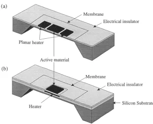
1.3.3 Application of Silicon Micromachining
Silicon Substrate Heater
(a)
Membrane
Electrical
Electrical insulator
Planar heater
Active material
r....-..,..., ---,-•
'
--',..,::----=---_---Membrane
Electrical insulator
over three-dimensional structures etched in the bulk. Surface micromachining
employs deposition and selective etching of sacrificial layers and thin films to produce
free-standing surface microstructures. Bulk micromachining techniques was
employed here to produce thermally insulated ultra-thin membrane structures. This
micromachined structure is referred to as a micro-hotplate (MHP). The heater can be
placed either in plane with the chemoresistor or embedded within the membrane, so
[image:31.595.125.437.257.510.2]allowing the chemoresistor to be superimposed above the microheater, as shown in
Figure 1.5.
Figure 1.5 Schematic of the different MHP arrangements, (a) MHP with the heater in plane with
microsensor, (b) MHP with embedded heater.
1.4 Research Objectives
The main objectives of this research are:
• To design and fabricate a number of silicon SADs for low power instruments.
• To characterise various gas-sensitive materials (e.g. MOS, XPc and CP) on these
silicon sensors to the gases of interest.
• To incorporate the developed SAD technology into an intelligent portable
1.5 Outline of Thesis
My thesis describes the design, fabrication, analysis and testing of novel chemoresistor designs for low-power instruments.
In Chapter 2 I introduce the typical characteristics of the gas-sensitive materials e.g. MOS, XPc and CP. The mechanisms that lead to the gas sensitivity of the different gas-sensitive materials investigated are outlined.
In Chapter 3 I describe the design of the different chemoresistive devices and the integrated MHPs. The sensor designs and choice of materials depend greatly on the fabrication procedures to be used. These fabrication techniques are therefore outlined in Chapter 4, which introduces the conventional planar and bulk micromachining techniques used to produce the inactivet device structure. This Chapter also describes the techniques used to deposit the gas-sensitive materials.
In Chapter 5 I discuss the modelling of chemoresistive gas sensors. The models presented are based on previous research. A model developed by Gardner [1.21] is outlined, which describes the theoretical response from a pair of chemoresistors adapted to give a self-diagnostic for long-term drift caused by poisoning. This novel feature has been implemented in one of the SADs described in Chapter 3.
The performance of the MHP structures is described in Chapter 6. Special design considerations are taken to minimise thermal power losses. Apart from describing the mechanisms of power consumption, a novel measurement technique is employed to measure the ultra-low thermal time constants. Modelling techniques are also applied (e.g. finite element methods and lumped-element methods) in order to describe both steady-state and transient thermal properties of MHP structures.
To characterise the gas sensors I have designed and developed an automated computer-controlled test system, which is described in Chapter 7. The system controls the concentration of CO, NO2, humidity and the operating temperature of each MHP. During the control of these variables it can measure the outputs from 12 gas sensors, the gas temperature, humidity and flow-rate. This test system is used to investigate the characteristics of chemoresistors coated with either Sn0 2 or XPc. A similar rig has been constructed elsewhere to test the CP devices.
In Chapter 8 I discuss the results obtained for the XPc and Sn0 2 chemoresistors, and the dual sensor device. In Chapter 9, I draw conclusions from the characteristics obtained for the SADs, allowing an intelligent sensor system employing a hybrid sensor to be broadly outlined. The research presented in this thesis has been the foundation for future work which is also discussed in Chapter 9.
1.6 References
1.1 Anon., Monitoring the Atmosphere in Underground Mines, Mining Magazine, December, 1988, 483-487.
1.2 E.R. Steyn, The Early Detection of Inflammable Gas at the Working Face,
Journal of the Mine Ventilation Society of South Africa, July, 1985, 81-82.
1.3 N. de Nevers, Air Pollution Control Engineering, McGraw-Hill, New York, 1995.
1.4 R.M. Harrison, A Fresh Look at Air, Chemistry in Britain, December 1994, 987-1000.
1.5 Health and Safety Executive, EH40/96 Occupational Exposure Limits 1996, HMSO, London, 1996.
1.6 Air Quality Guidelines for Europe, WHO Regional Publications, European Series No. 23 (1987) 210 (WHO, Copenhagen).
1.7 R.W. Bogue, Environmental Sensors: Present Practices and Future Prospects,
Proceedings of the VII Conf. on Sensors and their Applications, 1995, 3-11.
1.8 J.W. Gardner and P.N. Bartlett (eds.), Sensors and Sensory Systems for an
Electronic Nose, Kluwer Academic Publishers, Dordrecht, Netherlands, 1992.
1.9 W. GOpel, J. Hesse and J.N. Zemel (eds.), A Comprehensive Survey, Volume 1
Fundamentals and General Aspects, VCH, Weinheim, 1989, p170-191.
1.10 J.L. Vossen and W. Kern, Thin Film Processes, Academic Press, Inc., London, 1978.
1.11 J.L. Vossen and W. Kern, Thin Film Processes II, Academic Press, Inc., London, 1991.
1.12 S. Middelhoek and S.A. Audet, Silicon Sensors, Academic Press, London, 1989. 1.13 J. Brignell and N. White, Intelligent Sensor Systems, IOP Publishing Ltd.,
1.14 W. Giipel, J. Hesse and J.N. Zemel (eds.), Sensors a Comprehensive Survey Vol.
2 Chemical and Biochemical Sensors Part I, VCH, Weinheim, 1991.
1.15 J.J. Miasik, A. Hooper and B.C. Tofield, Conducting Polymer Gas Sensors, J.
Chem. Soc., Faraday Trans. 1, 82 (1986) 1117-1126.
1.16 P.N. Bartlett and S.K. Ling-Chung, Conducting Polymer Gas Sensors Part II:
Response of Polypyrrole to Methanol Vapour, Sensors and Actuators, 19 (1989) 141-150.
1.17 W. Giipel and K.D. Schierbaum, Sn02 Sensors: Current Status and Future Prospects, Sensors and Actuators B, 26-27 (1995) 1-12.
1.18 S. Zaromb and J.R. Stetter, Theoretical Basis for Identification and Measurement of Air Contaminants Using an Array of Sensors having Partly Overlapping Selectivities, Sensors and Actuators, 6 (1984) 225-243.
1.19 J.W. Gardner, Detection of Vapours and Odours from a Multisensor Array Using Pattern Recognition Part I. Principle Component and Cluster Analysis,
Sensors and Actuators B, 4 (1991) 109-115.
1.20 P. McGeehin, P.T. Moseley and D.E. Williams, Self-Diagnostic Solid State Gas Sensors Employing Both Model and Novel Materials, 6th Int. Congr. Sensors
and Systems Technology (Sensor-93), Nuremberg, Germany, 11-14 Oct. 1993,
ACS, Wunstorf, 1993, 113-125.
1.21 J.W. Gardner, Intelligent Gas Sensing Using an Integrated Sensor Pair, Sensors
and Actuators B, 26-27 (1995) 261-266.
1.22 P.T. Moseley and B.C. Tofield, Solid State Gas Sensors, Adam Hilger, Bristol, 1987, p 17-31.
1.23 Figaro Engineering Inc., Figaro Gas Sensors Products Catalogue, April 1995. 1.24 S.K.H. Fung, Z. Tand, P.C.H. Chan, J.K.O. Sin and P.W. Cheung, Thermal
Analysis and Design of a Micro-Hotplate for Integrated Gas Sensor Applications, Proc. Eurosensors IX, Stockholm, Sweden, 25-28 June 1995. 1.25 U. Dibbern, A Substrate for Thin-Film Gas Sensors in Microelectronic
Technology, Sensors and Actuators B, 2 (1990) 63-70.
1.26 V. Demame and A. Grisel, An Integrated Low-Power Thin-Film CO Gas Sensor on Silicon, Sensors and Actuators, 4 (1991) 539-543.
Chapter 2
2. Gas Sensing Materials
2.1 Introduction
The objective of this Chapter is to discuss the basic gas-sensing mechanisms of MOS, XPc and CP films, which are employed in chemoresistive gas sensors for the suitable detection of CO, NO 2 and VOCs.
The operation of a chemoresistor relies on the detection of a change in electrical resistance or conductance on exposure to particular molecules. The electrical conductance of a microsensor is the sum of the contributions from the conductances of the sensitive film (bulk effect) and the interfacial region between the gas-sensitive film and both the electrodes and substrate (contact effects). A change in the environmental conditions (e.g. gas concentration, temperature and humidity) will therefore be detected when either the bulk or contact conductance is affected.
The substrate material is chosen to be electrically insulating and so the conductance of the sensor is determined by the conductivity of the gas-sensitive material and electrode structure. However, the gas-sensitive film must adhere well to the substrate and provide a mechanically-robust device.
(chemisorbed) molecules. In a Schottky diode sensor this interface defines the dominant gas-sensitive mechanism.
The contribution to the sensor signal by the contact resistance can be minimised by careful control of the electrode deposition conditions and by optimising the electrode geometry [2.3].
The geometry of the sensor may change due to induced stresses. However, the substrate structure, materials and fabrication techniques are selected to minimise induced stress, as described further in Chapter 3. An example of induced stress has been exhibited in CPs, which can swell when exposed to high sorbate concentrations. In this case, the internal stresses throughout the microsensor will depend upon the gas concentration and temperature, which may lead to a deformation of the microstructure.
In this Chapter only the gas-sensitive film conductance (or resistance) is considered, because careful choice of the chemoresistor structure and materials renders the other contributing conductances (e.g. contact and electrodes) either insensitive to the gases of interest or negligible compared to the gas-sensitive film. In order to understand the gas-sensing characteristics of the MOS, XPc and CP chemoresistors investigated in this research, the mechanisms suggested by other researchers are reviewed. The effect of film composition and morphology on the chemoresistor characteristics is also outlined.
2.2 Metal Oxide Semiconductor Materials
There are a wide variety of MOS materials which have shown a sensitivity to changes in particular gases [2.4, 2.5]. The group of oxides considered here are those which operate from approximately 200°C to 600°C, where the dominant gas-sensing mechanisms occur at the surface (this includes internal surfaces for porous MOS films). The most successful type of MOS material (both in terms of sensor performance and commercially) have been the oxides of transition metals, in particular tin dioxide (Sn02). These materials have been employed in applications requiring the detection of low concentrations of potentially hazardous gases, in an atmosphere of steady partial pressure of oxygen (in air).
involved have been widely investigated. 5n0 2 is described as a model example, since it has been the most extensively studied and well understood of the metal oxides. Sn02 is most commonly employed in chemoresistors as thick or thin polycrystalline films. The deposition techniques used for thin and thick Sn0 2 films investigated here are discussed in Chapter 4.
As mentioned above the film morphology and composition (e.g. the effect of additives) are key parameters in determining the chemoresistor properties, as will be described in more detail later. However, to simplify the discussion involving the interaction of Sn0 2 with the gases of interest, the material is first considered as a pure thin film of single crystal Sn02.
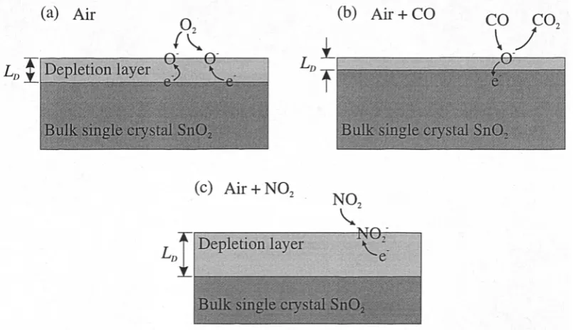
2.2.1 Gas Sensing Mechanisms of Single Crystal Sn02
The bulk of the thin Sn0 2 single crystal is typically a n-type semiconductor. The intrinsic donors are connected with a stoichiometric excess of metal (Sn), generating oxygen vacancies [2.6]. At elevated temperatures, an increasing fraction of the electrons bound by the bulk defects enter the conduction band. However, it is known that, at the temperatures of interest (< 600°C), the dominant mechanism causing conduction change is gas adsorption onto the crystal surface. If the adsorbing species is an oxidising gas (i.e. electron accepting) then chemisorption produces surface acceptors which bind electrons from the bulk. This causes a surface depletion region. Conversely, the chemisorption of a reducing gas (i.e. electron donating) leads to the production of surface donors, which release electrons to the bulk, so generating an accumulation layer. It is well known that in clean air, the chemisorption of oxygen (02) onto Sn02 removes electrons from the bulk, so forming negatively charged surface ions (e.g. 0 2-, 0- and 02") according to [2.7],
0 2 + e - <=> (0 -21d, (2.1)
(Oi Lis + e - <=> (20 - ) ads (2.2)
The rates of these reactions are dependent on temperature. Above approximately 180°C 0- ions are found as the prevailing species [2.8]. At even higher temperatures,
the adsorbed 0" species may form a 02- which becomes stable at a lattice site.
The depletion region which is formed in air has a depth of approximately 1 to 100 nm [2.9], and tends to increase the crystal's resistance. The thickness of the depletion layer is referred to as the Debye length (LD). Oxygen is always present in
the air, so the formation of an accumulation layer will not occur in the investigations presented here. The energy diagram, as is shown in Figure 2.1, has been used to model the surface interaction with 02 [2.6, 2.8].
Vacuum _ Oxidising, _— gas
Ionised donors
++
+ SnO, crystal
++
=
0 >-, 1-4 a-, bp
Ci 1-1 CD CU ,—. 0
W C1)
Surface acceptors
Depletion region
E,
[image:39.595.205.359.284.436.2]E,
Figure 2.1 Interaction of oxidising gas species (e.g. 02) with surface states causing depletion of surface
charge. This is indicated by the schematic distribution of charge (top diagram) and the band scheme
(bottom diagram) near the conduction band edge Ec, where EF is the Fermi level.
(a) Air
O
/
0 0 Depletion layer
c _
Bulk single crystal SnO,
I
(b) Air + CO L„
CO CO.
iO
Bulk single crystal SnO,
(c) Air + NO,
NO, Depletion layer NO,
Bulk single crystal SnO,
[image:40.595.81.484.70.302.2]L„:
Figure 2.2 Schematic showing the depletion layer in single crystal Sn02 in (a) air, (b) reducing gas
(e.g. CO) and (c) oxidising gas (e.g. NO2). Not all the surface interactions have been shown for the sake of clarity.
Our current understanding of surface reactions has been reviewed by Kohl [2.8]. In general, a reducing gas reacts with the adsorbed oxygen ions. The product of this reaction is desorbed from the surface, which releases electrons back to the conduction band and leaves a surface site available for further chemisorption with atmospheric oxygen. At equilibrium the concentration of adsorbed oxygen ions has been reduced and the depletion thickness falls. For example, a reducing gas of key interest here is CO. The main CO detection mechanism by the single crystal Sn02 is an irreversible combustion process described according to [2.7],
+ (Ol ads —> CO2 + (2.4)
greater charge depletion which increases resistance [2.10]. For example, the chemisorption of NO2 molecules by the capture of conduction band electrons from the single crystal Sn02 can be expressed as,
NO 2 + e - <=> (NO)
It has been postulated by Sayago et al. [2.11] that the NO2 can also be adsorbed
via interactions with the adsorbed 02- and 0- species.
The effect of water vapour has been widely studied, because it is present in most applications of interest [2.12]. The effect of water is known to induce electron injection at the temperatures of interest. One such adsorption mechanism with water may proceed according to,
H 2 0 + (0 - ) ads <=> 2(OH - ) ads + e - (2.6)
Several qualitative models have been proposed in the literature which explain the interaction of reducing gases in the presence of water [2.13, 2.8].
The gas adsorption examples presented so far are simplified atomistic models of a more complex microsystem. This is because the mechanisms also depend on a wide variety of other conditions e.g. temperature, catalytic dopants, microstructure and other species present on the surface and in the atmosphere. However, some of the interactive mechanisms are not fully understood. There may be several steps involved leading to the equilibrium with different chemisorbed gas species. Of the different reaction steps leading to the change in conductivity, the rate limiting process kinetics determine the sensor's response time. Different rate limiting process kinetics are thought to be involved during exposure and removal of the target gas, resulting in different 'on' and 'off' transients, respectively. The response time depends on many parameters, but at the temperature of highest sensitivity, MOS chemoresistors typically reach a steady-state value after a few tens of seconds.
have been deposited by thin film techniques (molecular beam epitaxy), but they still exhibit low sensitivities [2.14]. However, both thick and thin films of polycrystalline Sn02 have shown high sensitivities to the gases of interest, which led researchers to postulate alternative gas-sensing mechanisms. These models are still based on the surface interactions with the gases of interest, but the importance of Sn0 2 morphology is introduced in governing charge transport through the polycrystalline structure. These effects of thin and thick films of Sn02 are outlined in the following Sections.
2.2.2 Thin Polycrystalline Films
The structure of Sn02 deposited by thin film techniques [2.15] are in general shown to be polycrystalline with randomly orientated crystallites. The size of these crystallites are dependent on the deposition technique and any post-thermal treatment. For example, Sanjines et al. [2.16] have shown that as-sputtered films are initially amorphous, however, annealing the films at 550°C for 2 hours, produces crystallites with an average diameter of 15 nm (nanocrystals).
For nanocrystals with diameters greater than LD, the depletion layer affects the
local electron concentration of the conduction path between nanocrystals at the surface of the film. This mechanism of effecting conduction at the intercrystallite region has been commonly modelled as a potential barrier across which charge has to pass. This mechanism is more commonly used to model thick film Sn0 2, as will be described in more detail in the following Section.
For nanocrystals with a diameter less than LD, the depletion layer penetrates the entire nanocrystal. Therefore, electron concentration changes drastically within the nanocrystals upon exposure to adsorbing species. A thin film composed of small nanocrystals can be modelled macroscopically as a homogeneous semiconductor, in which the energy level of the conduction band edge at the surface is modulated by the charge transfer with adsorbing gas species [2.17]. This macroscopic model is equivalent to the single crystal model.
2.2.3 Thick Polycrystalline Porous Films
Chemisorbed species forming depletion layer (a)
E,
E,
[2.19]). This sensitivity cannot be ascribed by the single-crystal thin-film model [2.8, 2.9]. Hence, as for the thin film Sn02, other mechanisms have been postulated which
are associated with the materials morphology. The structure of porous thick film Sn02 is usually composed of grains with an average size of — 3 gm. These grains are
themselves composed of the nanocrystals described in the previous Section [2.9]. The gas can diffuse through the porous film, whereupon, it may adsorb with internal surface sites.
Classical methods of explaining the high sensitivity to certain gases were based on the morphology of the larger grains as explained below.
[image:43.595.184.433.392.611.2]It has been suggested that the conductivity is predominantly determined by the grain boundaries, the number of which is determined by the size of grains. If the grains touch but are not sintered, then the depletion layer forms a Schottky barrier, over which the charge-carriers must flow to transfer from one grain to the next, as is shown in Figure 2.3.
Figure 2.3 Grain boundary effects showing (a) a schematic of the grain boundaries with chemisorbed
02 forming a depletion layer that penetrates the grain (shaded region), (b) band scheme near the
conduction band showing the potential barrier (eV s) at grain boundaries. For simplification only 0702"
surface species are shown here.
Chemisorbed species forming depletion layer
Fully depleted
neck Neck with restricted
channel for current flow
lowered by the chemisorption of a gas then the potential barrier is also decreased, which corresponds to a lower resistance.
The properties of a Sn02 film are highly dependent on a high temperature (— 600°C to 700°C) sintering stage [2.9]. Sintering increases the strength of the initially deposited material by generating "necks" between adjacent grains. If the thickness of these necks are comparable to LD, then the adsorption of gases on the
necks has the same effect on conductance as adsorption on thin single crystal Sn02 films. An increase in LD has an effect of restricting the width of the neck channel
through which current flows, as shown in Figure 2.4. If the necks are thin enough, then all the carriers in the neck region are extracted, and the carriers must overcome a potential barrier to traverse the neck, which as before is modulated by the interaction of gas species at the surface.
Figure 2.4 Schematic showing the surface mechanisms involving intergranular necks. For
simplification only 0102" surface species are shown here.
More recently, Schierbaum et al. [2.20] have suggested possible conductance contributions by the nanocyrstals. In this case the negative surface charge due to the adsorbed negative oxygen ions causes depletion throughout entire nanocrystals at the internal surfaces.
conductance. Control of these properties is dependent on the deposition processes, but in most cases the reproducibility of sensor conductance is poor. The base-line resistances for 5n02 chemoresistors investigated in the literature therefore varies greatly (e.g. approximately 103 to 107 S2).
2.2.4 Effects of Catalytic Additives
It is known that Sn0 2 is sensitive to a wide variety of different gases, and so the poor specificity of MOS chemoresistors has limited their application. The specificity between some gases can be enhanced by careful choice of the operating temperature, but its effectiveness is limited. An alternative method to improve specificity is by the inclusion of catalytic additives or dopants [2.21, 2.22]. Two different types of sensitisation mechanism have been identified by Yamazoe et al. [2.22]. The first is a chemical interaction (catalytic) by which additives assist the redox processes leading to the interaction of the target gas. The second interaction is an electronic one, in which an additive behaves as a sort of electron donor or acceptor. The most commonly used additives in MOS films are palladium (Pd) and platinum (Pt), which have been shown to exhibit a catalytic chemical interaction. These additives form sites on the Sn02 surface which may activate the gases for detection at a faster rate than at the Sn02 surface. The ions formed on the catalyst site can then 'spillover' onto the Sn02 surface. The catalyst additives can therefore provide an alternative reaction kinetic path for the gas adsorption at a faster rate and with different activation energies (which changes the temperature of maximum sensitivity).
Both thin 5n02 and thick Sn02 films have been deposited onto my chemoresistor designs and their response to CO and NO 2 studied. Moreover, the effect of adding small amounts of Pd and Pt to the pure material has been analysed.
2.3 Organic Materials
2.3.1 Metal-Substituted Phthalocyanine Materials
2.3.1.1 XPc Structure
Phthalocyanines are highly coloured hetero-atom macro-cycles, in which two central hydrogen atoms can be substituted by a metal atom in the centre of a molecular ring, as shown in Figure 2.5. Where the metal species substituted into the molecule is represented by an 'X'. Note that if reference is made to a particular metal then the 'X' is replaced by the elements chemical symbol.
CNC I II N
C N
%*... X ZN—CN NC=N N—C 'N
I
[image:46.595.208.355.267.411.2]ci II C...s.„.N.,...,._._„k„
Figure 2.5 Structure of metal-substituted phthalocyanine (XPc) molecule.
2.3.1.2 Effect of Gases on Electrical Conductivity
XPcs behave in a similar manner to a p-type semiconductor. The actual charge carrying mechanisms associated with molecular crystals are beyond the scope of this review, the reader is refered to the work of Gutmann [2.23] and Wright [2.26] for further explanation of this topic. However, it is sufficient to note that the electrical properties and gas sensitivity of XPc films are strongly dependent on crystal structure and morphology.
The sorption of gases and vapours onto organic materials exert a profound influence on the conductivity. For XPc films the mechanisms responsible for conductivity changes are generally accepted as being dominated by gas adsorption. It is thought that oxidising gases influence conductivity via surface charge-transfer interactions, which generate charge carrying positive holes. For p-type XPcs the majority carriers in vacuum conditions are holes, so that exposure to an oxidising (i.e. electron-accepting) gas will increase the carrier concentration and hence, conductivity. As a result of these surface processes, the carrier concentration (thus the conductivity) in the bulk of the solid may change by several orders of magnitude due to the interaction of an adsorbed gas. The interactions between an oxidising gas and XPc can be described by the following general equilibria,
physisorption charge transfer
gas + XPc <=> G + XPc <=> , delocalisation
[G - XPci+ <=> [G - XPc] + hole
where G is a physisorbed molecule and G - is an ionised gas molecule.
The interactions of equation 2.7 are observed when XPc films are initially exposed to air, because the electron-accepting 0 2 molecules chemisorb onto the XPc surface. Thus, under normal atmospheric conditions XPc surfaces can be assumed to be completely covered with an adsorbed layer comprising mainly of 0 2 ions. Note that Mocket et al. [2.27] have postulated that the presence of adsorbed water-derived species is also essential for reversible 0 2 chemisorption.
For chemisorption to occur with another gas, an 0 2 surface site must first be made available by 0 2 desorption. XPc films have shown greatest sensitivity to gases with a high electron affinity, e.g. NO 2, NO, C12, F2. Their sensitivity to NO2 is of
greatest interest, because it is a common environmental pollutant. The surface charge-transfer due to NO2 chemisorption is stronger than existed previously with the chemisorbed 02 leading to an increase in conductivity. In contrast, chemisorption of a reducing gas (e.g. CO) leads to the extraction of p-type carriers and produces a conductivity decrease [2.28]. The strength of the surface charge-transfer interactions is the most important factor controlling the change in conductivity. If the interactions are too weak (physisorption) their effect on the activation energy for carrier generation is small and conduction enhancement is small. If, however, the interactions are too strong and localised (chemical bonding) the charge carriers are bound to the adsorption sites, so conduction enhancement is again small.
The rate of conductivity change upon exposure to a gas and the rate of its reversal in clean conditions, i.e. when the target gas is removed, are optimised when the interaction with the absorbant is weak. While the reversal will be faster for more weakly-bound gases, the chemisorption of a gas is primarily limited kinetically by the ease of displacement of adsorbed 0 2 from the surface. The kinetic factors that influence conductivity are temperature dependent. Archer et al. [2.25] suggest that thermal-treatment and gas-exposure history also contributes significantly to the response characteristics. As is mentioned earlier, thermal-treatment is known to modify the materials morphology and as a consequence changes both the conductivity and rate of sorption [2.24]. The temperature which optimises response rate, reversibility and selectivity, while retaining reasonable sensitivity and device lifetime, is usually determined experimentally.
2.3.1.3 Typical Characteristics of XPc Chemoresistors
gases other than NO 2 e.g. H2S and HC1. All these materials were deposited at the Health and Safety Executive (HSE), Sheffield.
Typical values of XPc film conductance (G) and sensitivity to NO 2 [2.29, 2.30] are shown in Table 2.1.
Table 2.1 Typical characteristics for XPc films deposited by vacuum sublimation. Material Range of G in 2.8 ppb
NO2 at 170°C (S2-1 )
AG(44 ppb)/G(2.8 ppb) x 100 at 170°C
(%)
Temperature of maximum sensitivity
(T)
PbPc 1.5 - 4.5 x 10⁻⁸ 185 —160
CuPc 3.0 - 4.5 x 10⁻⁸ 100 —160
MgPc 5.3 - 6.9 x 10⁻⁶ 5
would be inadequate for an instrument warning against short term exposure hazards. Despite high sensitivity, XPc chemoresistors also suffer from poor long term stability
and reproducibility, which have limited their use in commercial sensors.
2.3.2 Conducting Polymer Materials
The observation of a high electrical conductivity in doped organic polymers has been known since the late 1970s. These materials are commonly referred to as conducting polymers (CPs) and may be ionic or electronic conductors. Several applications have been envisaged for CPs (e.g. battery electrodes, electromagnetic shield, displays, and conducting plastics). The change in conductivity of electronically-conducting aromatic and heterocyclic polymers when exposed to various vapours (e.g. VOCs) has generated great interest for sensing applications [2.33]. The ease with which these kind of CPs can be electrochemically deposited as thin films and coupled with their good thermal stability makes them attractive for chemoresistive applications.
Although CP chemoresistors have a lower sensitivity (with a change in resistance up to approximately ± 10 %) when compared to MOS and XPc films, they do respond to vapours very rapidly (typically less than 10 s) at RT. However, since these materials are sensitive to a wide range of vapours, the specificity of an individual CP chemoresistor is poor. It is very easy to produce a CP chemoresistor with a base-line resistance suitable for simple interface electronics, because their conductivities are very high (in the order of 10 -5 S/m [2.34]) and controllable by the deposition conditions.
(a)
(b)
N n
Figure 2.6 The generally accepted structures of (a) PPy, and (b) PAn.
In its oxidised state pyrrole exists as a polycation. The charge on the polymer is balanced by doping (i.e. the incorporation of anions) the film during electrochemical preparation. As a result the electrical characteristics, gas-sensing properties and structure of the final polymer depends on the choice of monomer and on the choice of counter-ion [2.37]. The counter-ions used in films that are at present being investigated (by the Universities of Warwick and Southampton Electronic Nose Group) are the alkylsulfonates (RSA, where the `R' refers to the length of the alkyl group, e.g. pentanesulfonate becomes PSA).
The mechanisms of gas-sensitivity in CPs are, at present, poorly understood. However, a sorption model (Langmuir adsorption isotherm) has been empirically shown to be a good description [2.35]. Where the vapour species (V) interacts with internal sites, according to
V + (site) <#.(V)
kb
where kr and kb are the forward and backward reaction rates, respectively. This sorption model is described in greater detail in Chapter 5, which outlines the modelling of chemoresistive gas sensors.
Several possible theoretical mechanisms are being investigated by researchers to discover a correlation with the empirical models. The theoretical explanations have envisaged swelling of the polymer, interaction between the gas molecules and the charge carriers on the polymer chain, gas molecule/counter-ion interactions and oxidation or reduction of the polymer by the gas. Bartlett et al. [2.38] has suggested five possible mechanisms which might contribute to the overall observed gas-sensitivity of a CP chemoresistor, as depicted in Figure 2.7.
Counter-ion
(2)
Adsorbed species
(3) ®
Conducting Polymer
(5)
[image:52.595.96.464.94.309.2]Metal Electrode
Figure 2.7 Possible mechanisms of the gas-sensitivity of CP chemoresistors caused by gas sorption, (1)
direct carrier generation or removal by oxidation or reduction, (2) change in intrachain carrier mobility,
(3) interaction with the counter-ion, (4) change in interchain hopping, (5) change in interfacial charge
transfer.
Once a better understanding of the gas-sensing mechanisms have been established, the sensor performance can be improved by exploiting the high degree of property control with the electrochemical deposition conditions.
2.4 Chemoresistor Design Considerations
The performance of a gas-sensitive material is known to be dependent on the structure of the chemoresistor, as described below.