University of Warwick institutional repository: http://go.warwick.ac.uk/wrap
A Thesis Submitted for the Degree of PhD at the University of Warwick
http://go.warwick.ac.uk/wrap/53742
This thesis is made available online and is protected by original copyright. Please scroll down to view the document itself.
Development and Application of
Pipet-Based Electrochemical Imaging
Techniques
Neil Ebejer
A thesis submitted for the degree of Doctor of Philosophy
The University of Warwick, Chemistry Department
ii
Table of Contents
Table of Contents...ii
List of Figures...vii
List of Tables...xxi
Acknowledgements...xxii
Declaration...xxiii
Abstract...xxv
Abbreviations...xxvi
CHAPTER 1...1
INTRODUCTION...1
1.1 Dynamic Electrochemistry...1
1.1.1 Electron transfer at the electrode...2
1.1.2 Mass transfer...4
1.1.2.1 Diffusion...5
1.1.2.2 Migration...7
1.1.2.3 Convection...7
1.1.3 Experimental electrochemistry...7
1.1.3.1 Macro electrodes...7
1.1.3.2 Cyclic Voltammetry...8
1.1.3.3 Amperometry...10
1.1.3.4 Potentiometry...10
1.2 Scanning Electrochemical Microscopy (SECM)...10
1.2.1 Instrumentation...12
iii
1.2.1.2 Probe positioning...14
1.2.1.3 Signal generating / acquiring devices...15
1.2.2 Modes of operation...15
1.2.2.1 Feedback mode...15
1.2.2.2 Generator collector mode...17
1.2.2.3 Permeability and ion transport at interfaces...18
1.2.2.4 Pipet based liquid / liquid interface probes...19
1.2.3 The issue of substrate topography...19
1.2.3.1 Scanning Electrochemical Microscopy - Atomic Force Microscopy (SECM-AFM)...20
1.2.3.2 Scanning Electrochemical Microscopy – Scanning Tunnelling Microscopy (SECM-STM)...21
1.2.3.3 Dual Mediator...22
1.2.3.4 Shear force SECM...22
1.2.3.5 Alternating Current Scanning Electrochemical Microscopy (AC-SECM)...24
1.2.3.6 Tip position modulation (TPM) – SECM...24
1.2.3.7 Intermittent Contact SECM (IC-SECM)...25
1.2.4 Application of SECM in real world systems...26
1.2.4.1 Soft stylus probe...26
1.2.4.2 SECM in Ionic Liquids...27
1.3 Scanning Ion Conductance Microscopy (SICM)...28
1.3.1 Probes...28
1.3.2 Modes of operation...28
1.3.2.1 Non modulated (dc) mode...29
1.3.2.2 Distance-modulated (ac) mode...29
1.3.2.3 Hopping mode...30
1.3.3 Applications of SICM...31
1.4 Chemical deposition using double barrel nanopipets...32
1.5 Scanning Electrochemical Microscopy – Scanning Ion Conductance Microscopy (SECM-SICM)...34
1.6 Pipet Based Electrochemical techniques...35
1.6.1 Techniques developed for localised corrosion studies...35
iv
1.6.3 Scanning Electrochemical Cell Micrsocopy (SECCM)………...40
1.7 Research aims...41
1.8 References...43
CHAPTER 2...48
Instrument Design, Construction and Experimental techniques...48
2.1 SECCM...48
2.2 Hardware...49
2.2.1 Data acquisition...49
2.2.2 Electronic Components...51
2.2.3 Probe oscillation electronics...53
2.2.4 Lock-in Amplifier...53
2.2.4.1 Phase Sensitive detection...54
2.3 Actuation and positioning...55
2.3.1 Piezoelectric positioners...55
2.3.2 Micromanipulators...57
2.4 Probes...57
2.4.1 SECCM probes...57
2.4.2 SECM – SICM probes...61
2.5 Optical visualisation...61
2.6 Humidity Cell...62
2.7 Faraday Cage...62
2.8 Software...63
2.8.1 Basic SubVIs...63
2.8.2 Scan program...64
2.8.3 Dual Channel CV program...67
2.9 Microscopy and spectroscopy...67
2.9.1 Atomic Force Microscopy (AFM)...67
2.9.2 Optical Microscopy...68
2.9.3 FE-SEM...68
2.9.4 Micro Raman Spectroscopy...69
v
2.10.1 Graphene synthesis and preparation...69
2.10.2 SWNT synthesis and preparation...70
2.10.3 Electrical contacts...72
2.11 Chemicals and materials...72
2.12 References...74
CHAPTER 3...75
Localised High Resolution Electrochemistry and Multifunctional Imaging: Scanning Electrochemical Cell Microscopy...75
3.1 Introduction...76
3.2 Experimental...79
3.2.1 SECCM setup...79
3.2.2 Sample preparation...79
3.2.3 Solutions and chemicals...79
3.3 Results and discussion...80
3.3.1 Tip approach measurements...80
3.3.2 Imaging with SECCM...81
3.3.3 Surface Amperometric imaging...84
3.3.4 Mapping of ion fluxes into biominerals...85
3.4 Advances in SECCM...86
3.4.1 FEM model...87
3.5 Conclusions...91
3.6 References...93
CHAPTER 4...94
Structural Correlations in Heterogeneous Electron Transfer at Monolayer and Multilayer Graphene Electrodes...94
4.1 Introduction...94
4.2 EC measurements with SECCM...96
vi
4.4 Complementary surface analysis...108
4.5 Conclusions...114
4.6 References...115
CHAPTER 5...117
High Resolution electrochemical interrogation of complex Single Walled Carbon Nanotube (SWNT) structures...117
5.1 Introduction...118
5.2 Results and discussion...120
5.2.1 3D forests...120
5.2.2 2D SWNT networks...128
5.3 Conclusions...146
5.4 References...148
CHAPTER 6...150
Fabrication and characterisation of dual barrel SECM – SICM probes...150
6.1 Introduction...150
6.2 Experimental...151
6.3 Results and discussion...152
6.4 Conclusions...160
6.5 Referneces...161
CHAPTER 7...162
vii
List of figures
Figure 1-1 A schematic of the processes undergone in basic dynamic
electrochemistry. 2
Figure 1-2 Energy level diagram. In case a) there is insufficient energy to reduce species, O, by tuning the Fermi level with an applied potential there is now sufficient energy for electron transfer between the metal
electrode and O to occur as in case b). 3
Figure 1-3 a) shows the linear diffusion profile towards a macroelectrode and b) shows a 3 electrode system where ref is the reference electrode and counter is the counter electrode bathed in solution and connected to a
potentiostat. 8
Figure 1-4 A typical waveform for a CV broken up into segments. The cycle goes from a negative potential to a positive one and vice versa. 8
Figure 1-5 Initially, the chemical reaction is governed by kinetics of the heterogeneous electron transfer across the electrode / solution interface. At the maximum the current response is due to diffusion.1
9
Figure 1-6 Schematic of the varied modes of application of SECM (top) and the current response observed in each (bottom), as normalised by the
current far from the surface. 12
Figure 1-7 A schematic of an SECM rig. 12
Figure 1-8 Optical microscope images of a UME from an end on view and side
viii
Figure 1-9 Schematic of a hemispherical diffusion field established for the steady state diffusion-limited oxidation of a bulk solution species. 14
Figure 1-10 A schematic of SECM operating in feedback mode when encountering a conducting and insulating substrate. 16
Figure 1-11 SECM operating in generator collector mode. 17
Figure 1-12 Inducing an interfacial process using feedback mode a) monitoring
induced transfer b). 18
Figure 1-13 A schematic showing dc mode SICM. 29
Figure 1-14 A schematic showing ac mode SICM. 30
Figure 1-15 A A schematic showing hopping mode SICM. 31
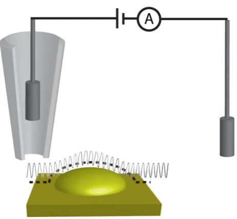
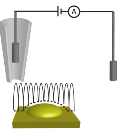
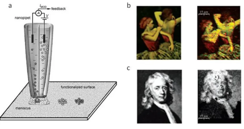
Figure 1-16 A schematic of the double barrel nanopipet system a), b) and c) are the original images (right) together with their patterned counterparts (left) using a two component graded deposition.104 34 Figure 1-17: A schematic of the experimental setup for the microcell reactor using a microscope for visualisation of the probe position. The expanded image to the right, shows the capillary connected up in a 3-electrode
system.108-109 36
ix
Figure 1-20: A schematic of the SMCM setup a) and optical image of the aluminium alloy b) and the corresponding electrochemical image
c).118 40
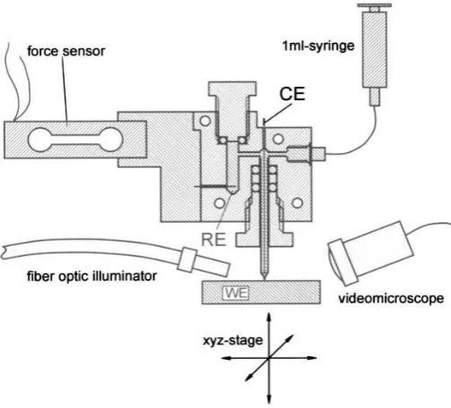
Figure 2-1 An optical image of the instrument, showing the components used in
SECCM. 49
Figure 2-2 A schematic of the original SECCM setup. 51
Figure 2-3 A schematic of the revised SECCM setup. 52
Figure 2-4 A schematic of a reference signal applied to a lock-in amplifier, the lock-in signal after performing the phase locked loop and the experimental signal with a slight phase shift from the reference. 54
Figure 2-5 An optical image of the laser puller with a zoom in, of the control
panel. 58
Figure 2-6 Optical image a) of a pulled 400 nm, borosilicate theta pipet, b) the corresponding SEM image, c) an SEM image of a 300 nm quartz theta pipet and d) an SEM image of a 100 nm quartz theta pipet. 60
Figure 2-7 A schematic of the humid cell used during experimentation. The sample is elevated so that a moat can be used to ensure a humid
x
Figure 2-8 A screenshot of the subVI called ‘measure and analyse’ and was part of frame 5. As can be seen input channels are split and processed
relaying the data to the main GUI. 65
Figure 2-9 Screenshots of different panels of the GUI. The top screenshot shows the approach settings and the graph in where 3-D topographical features could be seen. The bottom screenshot shows the feedback panel where the user could adjust the gains with the feedback parameter plotted in an x-y chart on the right. 66
Figure 3-1 Schematic (not to scale) of the theta pipet system which serves as a localized conductivity cell (measurement of iDC and iAC) and for
conducting/semiconducting surfaces as a local dynamic
electrochemical cell (isurf). 77
Figure 3-2 a) Typical pipet approach data showing iDC (black) and iAC (red) as a
theta pipet was translated towards a glass surface, until surface contact was made. A bias of 500 mV was applied with 20 mM KCl in the pipet. Note the log current scale. b) A zoom of the final few points of iDC and iAC until contact of the electrolyte from the pipet cell with
the surface.
81
Figure 3-3 SECCM images of gold bands on glass. (a) 3D topography of the sample. (b) Plane fitted topographical data from (a). (c) iDC image in
xi
Figure 3-4 (a) Surface current maps of the gold band structure. (a) 20 mM KCl; (b) 2 mM FcTMA+ , 20 mM KCl. The substrate was at biased at +500 mV with respect to the Ag/AgCl quasi-reference electrode. 85
Figure 3-5 Topographical image (a) of the enamel surface (plane fitted) and (b) corresponding iDC image of the same region acquired simultaneously.
86
Figure 3-6 Schematics of (a) the SECCM setup showing key geometric dimensions and electronic circuits and (b) the simulation domain. Not
to scale. 88
Figure 3-7 Simultaneously recorded ion conductance currents (a,b) and the working electrode response (c,d) during CV measurements (v = 100 mVs-1) for the FcTMA+/2+ couple on HOPG. The currents between the two QRCEs in each barrel (experimentally and ib and simulated iic
(a,b)) and the working electrode response(iWE and iWE,lim) were
recorded as a function of Et for different values of Eb between 0 and
0.5 V (marked on (a) and (c)). The probe was defined by rp = 0.6 µm
and ϴ = 8.5, mh = 0.15 µm filled with 2 mM FcTMA+ and 50 mM
KCl. Plot (e) is a magnified view of the ion current between barrels, ib, at bias 0.5 V (from plot (a)), where a change in ib is observed. The
change in ic during voltammetric sweeps is plotted as a function of the
bias potential for experimental and simulated data sets (f). Experimental (colored circles) and simulated data (stars) are plotted
for (b), (d), and (f). 90
xii
1.1 μm diameter pipet. (c) Optical microscope image of the CVD graphene area mapped by SECCM, showing the heterogeneity of the surface and the presence of multiplelayer graphene flakes. (d) Set of three EC maps of the area shown in (c) acquired by SECCM at three different substrate electrode potentials (E-Eº) indicated in LSV in (b) with labels E1, E2 and E3. All images are at the same scale as (c). The
arrow-circle in part (c) and (d) indicates a small area where the SIO2
was exposed and measured currents in this area are below the lower limit on the scale bar. This area was used to calibrate the number of
graphene layers (vide infra). 97
Figure 4-2 Optical image (a) and its corresponding image using the green component of the RGB scheme (b) of the CVD graphene area studied. The red square marks an area where bare SiO2/Si is exposed and the
green square marks an area with 4 different thickness graphene flakes. (c) Histogram of the green component of each area marked with red and green squares. (d) Calibration plot of green component, light
contrast and number of graphene layers. 99
Figure 4-3 Set of maps obtained during SECCM scanning at a potential E = -0.15 V. (a) z-piezo displacement from which topography can be observed, (b) AC component of the ion current barrels (c) conductance current between barrels, (d) electrochemical current at the working electrode, (e) pixel-by-pixel correlation between EC current map and the corresponding optical image of the scanned area, averaged and converted to green component. Scale bar is 20 µm. The points corresponding to Si/SiO2 were discarded. The arrow-circle in (d)
marks a small area where the silicon oxide was exposed due to a hole
xiii
Figure 4-4 Set of maps obtained during SECCM scanning at a potential E = -0.043 V. (a) z-piezo displacement from which topography can be observed, (b) AC component of the ion current barrels (c) conductance current between barrels, (d) electrochemical current at the working electrode, (e) pixel-by-pixel correlation between EC current map and the corresponding optical image of the scanned area, averaged and converted to green component. Scale bar is 20 µm. The points corresponding to Si/SiO2 were discarded. The arrow-circle in
(d) marks a small area where the silicon oxide was exposed due to a
hole in the CVD graphene layer. 101
Figure 4-5: Set of maps obtained during SECCM scanning at a potential E = 0.016 V. (a) z-piezo displacement from which topography can be observed, (b) AC component of the ion current barrels (c) conductance current between barrels, (d) electrochemical current at the working electrode, (e) pixel-by-pixel correlation between EC current map and the corresponding optical image of the scanned area, averaged and converted to green component. Scale bar is 20 µm. The points corresponding to Si/SiO2 were discarded. The arrow-circle in
(d) marks a small area where the silicon oxide was exposed due to a
hole in the CVD graphene layer. 102
Figure 4-6: Set of maps obtained during SECCM scanning at a potential E = 0.065V. (a) z-piezo displacement from which topography can be observed, (b) AC component of the ion current barrels (c) conductance current between barrels, (d) electrochemical current at the working electrode, (e) pixel-by-pixel correlation between EC current map and the corresponding optical image of the scanned area, averaged and converted to green component. Scale bar is 20 µm. The points corresponding to Si/SiO2 were discarded. The arrow-circle in
(d) marks a small area where the silicon oxide was exposed due to a
xiv
Figure 4-7 Set of maps obtained during SECCM scanning at a potential E = 0.2 V. (a) z-piezo displacement from which topography can be observed, (b) AC component of the ion current barrels (c) conductance current between barrels, (d) electrochemical current at the working electrode, (e) pixel-by-pixel correlation between EC current map and the corresponding optical image of the scanned area, averaged and converted to green component. Scale bar is 20 µm. The points corresponding to Si/SiO2 were discarded. The arrow-circle in (d)
marks a small area where the silicon oxide was exposed due to a hole
in the CVD graphene layer. 104
Figure 4-8 Schematic of the SECCM probe and sample (not to scale) showing
the key geometric dimensions as described previously in Chapter 3. 103 105
Figure 4-9 FE-SEM images of the SECCM probes used to obtain maps of graphene. Scale bar is 1 µm and tw = 50 nm. 105
Figure 4-10 FEM model determined approach curves for the SECCM probe, with an oscillation amplitude (peak to peak) of 100nm. 106
Figure 4-11 Boltzmann fits for the simulated k0 values obtained by FEM modelling of the SECCM probe at (a) Eop = -0.065 V; (b) Eop = -0.016
V and (c) Eop = 0.043 V. The shadowed area indicates the range of
currents where the reaction is essentially reversible (within experimental error), indicated by the shaded zones in figure 4-11. 107
xv
current and standard rate constant, k0, for each defined number of CVD graphene layers, for potentials E1, E2, and E3 (from left to right). The dashed line in (a) and the blue area in (b) denote the conditions where the ET process becomes entirely reversible. 109
Figure 4-13 (a) Optical image of CVD graphene with four different flakes labeled A1, A2, A3, and A4, and corresponding SECCM data. Scale bar is 5 μm. (b) Histograms of the EC current in each designated flake at potential E2. (c) Raman spectra acquired with an excitation wavelength of 633 nm and spot size of 500 nm at each graphene flake. The three characteristic Raman peaks for graphene are labeled as D, G, and 2D. (d) Raman 2D peak for regions A1 (red line) and A2 (blue line) plotted together highlighting the ∼10 cm−1 Raman upshift characteristic for a non-AB stacking bilayer (blue line). Schematic of Bernal (AB-stacking) for a bilayer of graphene. The basic structure of graphene is defined with two atoms in the unit cell, denoted A (red dot) and B (blue dot). For an AB stacking bilayer, the A atom of the top layer lies directly over the B atom of the bottom layer. (e)The Raman 2D peak for areas A1 (red line), A3 (green line), and A4
(orange line). 111
Figure 4-14 Zoom of the optical microscope image and the associated SECCM maps at all potentials (E1, E2, E3) of the area examined with Raman spectroscopy. Four different areas are labelled as A1, A2, A3, and A4, and their histograms of EC current are shown. 112
Figure 4-15 AFM images of the CVD graphene studied by SECCM. The black
xvi
Figure 5-1 (a) FE-SEM image of a SWNT forest. (b) typical TEM image of a
SWNT extracted from a forest. 121
Figure 5-2 Micro-Raman spectra of an intact SWNT forest focusing on the
sidewalls and tube ends. 122
Figure 5-3 (a) XPS spectra of bare catalyst substrate (red line) and SWNT forest surface (black line). The inset shows the spectral range corresponding to Co 2p3/2 for both SWNT forest (black line) and catalyst (red line)
surfaces. (b) Typical TEM image of SWNT ends. 123
Figure 5-4 a) Digital photograph and schematic of the pipet in contact with the forest sidewalls, for voltammetric and conductance analysis. b) Current-voltage curves (forward and reverse) recorded on the closed ends (blue) and sidewalls (red), with a pipet of inner diameter 400 nm, containing 50 mM KCl at 100 mV s-1. 124 Figure 5-5 Typical CVs of 5 mM Ru(NH3)63+ reduction in 50 mM KCl at a scan
rate of 100 mV s-1. Red lines indicate forest sidewalls, blue lines,
forest closed ends. 126
Figure 5-6 CVs of 2 mM FcTMA+/2+ oxidation in 50 mM KCl at a scan rate of 100 mV s-1. Red lines indicate forest sidewalls, blue lines, the forest
closed ends. 127
xvii
expanded image of a junction and a bundle splitting. Catalyst particles can be seen in the AFM image but are not connected to the SWNTs and are electrochemically inactive. 129
Figure 5-8 Raman spectra for the SWNT network on a Si/SiO2 substrate. 130
Figure 5-9 Experimental data obtained using SECCM of the SWNT network. SECCM images (2.5 µm x 2.5 µm) of SWNT networks at the formal potential for FcTMA+/2+ (2 mM) (a) and Ru(NH3)63+/2+ (5 mM) (b).
Representative trace (a, b) and retrace (b) linescans are shown below. 131
Figure 5-10 CV (left) and LSV (right) on HOPG employing the SECCM setup, for 2 mM FcTMA+ and 5 mM Ru(NH3)63+, respectively in phosphate
buffer. 130
Figure 5-11 Forward (trace) and reverse (retrace) scans of an EC map on a SWNT network for Ru(NH3)63+ reduction at the formal potential. The image
area is 2.5 µm x 2.5 µm. 132
Figure 5-12 Four complementary maps obtained by SECCM simultaneously on a SWNT network for FcTMA+ oxidation at the formal potential. (a) EC current, (b) ion current, (c) AC component of the ion current, and (d) z-displacement of the SECCM probe (flattened). 134
Figure 5-13 Four maps obtained by SECCM simultaneously on a SWNT network for Ru(NH3)63+ reduction. (a) EC current, (b) ion current, (c) AC
component of the ion current, and (d) z-displacement of the SECCM
probe (flattened). 135
xviii
component of the ion current, and (d) z-displacement of the SECCM
probe (flattened). 136
Figure 5-15 Effect of tip-sample separation on the EC response of an SWNT of wnt = 1.5 nm, held at the formal potential and positioned in the center
of the SECCM meniscus. The pipet was of radius, rp = 125 nm, filled
with 5 mM Ru(NH3)63+ and 50 mM phosphate buffer solution (pH
7.2) and a barrel current of 1 nA for all heights. The response is
shown for different k0indicated. 139
Figure 5-16 Summary of the experimental peak EC current data and simulation results. (a) The SWNT height distribution from the AFM images. Histograms of peak current populations from SECCM images for Ru(NH3)63+ reduction (red) and FcTMA+ oxidation (green) from
regions of the image where individual SWNT peaks were identified. For Ru(NH3)63+ reduction the peak current population is also shown
for points where more than one nanotube is under the tip (crossed SWNT), (b) and (c) Working curves of EC current vs standard rate constant for HET at a fully active individual SWNT of height 1 nm with Ru(NH3)63+ and FcTMA+ as the redox mediator, respectively.
The simulations were at the formal potential and a transfer coefficient of α = 0.5 was assumed. 140
Figure 5-17 Effect of the simulated SWNT width (equivalent height) on the working electrode current for Ru(NH3)63+ reduction (k0 = 4 cm s-1)
xix
for the current response of an SECCM probe translated over a portion of an individual SWNT, compared to simulations for full sidewall activity (blue, k0 = 4 cm s-1), one active defect (red, k0 = 100 cm s-1) and three active defects (green, k0 = 100 cm s-1). 145 Figure 6-1 A Schematic of the setup used to fabricate DBCNP. 152
Figure 6-2 An optical image of the holder used for DBCNP fabrication. 152
Figure 6-3 Raman spectra of the deposited carbon with one of the dual capillary channels. Black line represents the effect of the omnifit sealing method compared to the ‘Blu Tack’ sealing method (red line). 153
Figure 6-4 SEM images of typical DBCNPs a) shows a DBCNP image after being used with salt crystals around the edges, b) a probe with the quartz end broken off10 and c) probes down to 20 nm total diameter.10
154
Figure 6-5 Typical cyclic voltammograms for the DBCNP. Parts a to c are performed using 10 mM Ruhex, whilst d is using 2 mM FcMeoH with a scan rate of 100 mV s-1 unless indicated. Figure b overlays two half of a pipet fabricated into carbon electrodes showing a high rate of reproducibility, with d showing similar behaviour for different scan
rates. 156
xx
Figure 6-7: Simultaneous topographical (left) and electrochemical (right) images. a) PET in 1 mM FcCH2OHinPBS. b) Pt interdigitated array in 1 m
FcCH2OH in PBS. c) Living sensory neurons in 0.5 mm FcCH2OH in
HBSS. The SECM and SICM electrodes were held at 500 and 200 mV versus a reference Ag/AgCl electrode, respectively. Electrochemical images were based on an oxidation current of
xxi
List of tables
Table 5-1 Values for mobility, charge and diffusion coefficient of solution
xxii
Acknowledgements
I would like to thank Professor Patrick Unwin, for his great supervision, guidance and importantly his patience. He has made my project truly enjoyable and I am really grateful for all the times I was pushed and steered in the right direction, none of this would have been possible without him. I would also like to thank Professor Julie Macpherson for her helpful discussions and supervision, providing criticism which I now truly appreciate.
I would laike to thank everyone on the Warwick Electrochemistry and Interfaces group for making my time here such an enjoyable one. We have had alot of laughs and experiences which I will never forget.
I thank Paul Kirkman and Robert Lazenby, for all the fun times and joking around, but also for always being around when no one else was. James Iacobini and Tom Miller thank you for your endless humour and for all the enjoyable times both at work and socially. Dr. Stanley Lai should be noted for his patience and for bringing stroopwafels. I would laike to thank Jon Newland for our endless gaming nights and helpful advice with photography and Dr. Petr Dudin for all the fun times.
I would especially like to thank Dr. Aleix Güell for mentoring me throughout the last few years. He has been a great source of inspiration, a fountain of knowledge when having scientific discussions and most importantly a great friend.
I would like to thank my sponsors at NPL, most notably Dr. Andy Pollard and Dr. Charles Clifford who were very helpful and welcoming, during my internship.
Last but not least, I would like to thank my parents for their constant support and for believing in me. I would also like to thank my sister Sarah who was always there when I needed a break, have a good laugh and alot of fun.
xxiii
Declaration
I declare that thesis consists of my own work except the following collaborations: i) Chapter 3. Simulations were carried out by Dr. Michael E. Snowden and experimental data was perfomed jointly with Dr. Aleix G. Güell. ii) Chapter 4. The synthesis and characterisation of the graphene samples were performed by Dr. Aleix G. Güell and the simulations were performed by Dr. Michael E. Snowden. ii) Chapter 5. SWNT forest samples were synthesised and characterised by Mr. Thomas S. Miller and the 2D SWNT networks were synthesised and characterised by Dr. Aleix G. Güell and the simulations were performed by Dr. Michael E. Snowden.
I declare that this thesis has not been submitted for a degree at any other university.
Parts of this thesis have appeared in the following publications:
Chapter 1 - Scanning Electrochemical Cell Microscopy – N. Ebejer, A. G. Güell, S. C. S. Lai, K. McKelvey, M. E. Snowden, P. R. Unwin - Annu. Rev. Anal. Chem (submitted)
Chapter 3 - Localized High Resolution Electrochemistry and Multifunctional Imaging: Scanning Electrochemical Cell Microscopy - N. Ebejer, M. Schnippering, A. W. Colburn, M. A. Edwards & P. R. Unwin, Anal. Chem., 2010, 82 (22),
9141-9145.
Chapter 3 - Scanning Electrochemical Cell Microscopy (SECCM): Theory and
Experiment for Quantitative High Resolution Spatially-Resolved Voltammetry and Simultaneous Ion-Conductance Measurements – M. E. Snowden, A. G. Güell, S. C. S. Lai, K. McKelvey, N. Ebejer, Michael A. O'Connell, Alex W. Colburn, and Patrick R. Unwin, Anal. Chem., 2012, 84 (5), 2483-2491.
Chapter 4 - Structural Correlations in Heterogeneous Electron Transfer at
xxiv
Snowden, J. V. Macpherson, P. R. Unwin, J. Am. Chem. Soc., 2012, 134 (17),
7258-7261. 6.
Chapter 5 - Nanoscale Visualization of Heterogeneous Electron Transfer Rates in
2-D carbon nanotube networks – A. G. Güell, N. Ebejer, M. E. Snowden, K. McKelvey, J. V. Macpherson, P. R. Unwin – Proc. Natl. Acad. Sci. USA, 2012, 109, 11487
Chapter 5 - Electrochemistry at Carbon Nanotube Forests: Sidewalls and Closed Ends Allow Fast Electron Transfer – T. S. Miller, N. Ebejer, A. G. Güell, J.V. Macpherson, P. R. Unwin – Chem. Comm., 2012, 48, 7435
Chapter 6 - Multifunctional Nanoprobes for Nanoscale Chemical Imaging and
xxv
Abstract
xxvi
Abbreviations
ADC analog to digital converter
AC-SECM alternating current – scanning electrochemical microscopy
AFM atomic force microscopy
CNT carbon nanotube
CPU central processing unit
CV cyclic voltammetry
CVD chemical vapour deposition
DAC digital to analog converter
DAQ data acquisition
DBCNP dual barrel carbon nanoprobe
EC-STM electrochemical scanning tunnelling microscopy
ET electron transfer
FE-SEM field emission – scanning electron microscope
FIB focussed ion beam
FPGA field programmable gate array
GUI graphical user interface
HET heterogeneous electron transfer
HOPG highly oriented pyrolytic graphite
IC-SECM intermittent contact scanning electrochemical microscopy
xxvii
LSV linear sweep voltammogram
LUMO lowest unoccupied molecular orbital
MWNT multiwalled carbon nanotube
NP nanoparticle
NSOM near field scanning optical microscopy
PC personal computer
QRCE quasi reference-counter electrode
SECCM scanning electrochemical cell microscopy
SECM scanning electrochemical microscopy
SECM-AFM scanning electrochemical microscopy – atomic force microscopy
SECM-SICM scanning electrochemical microscopy – scanning ion conductance microscopy
SECM-STM scanning electrochemical microscopy – scanning tunnelling microscopy
SEM scanning electron microscope
SG-TC substrate generation – tip collection
SICM scanning ion conductance microscopy
SMCM scanning micropipette contact method
SPM scanned probe microscopy
STM scanning tunnelling microscopy
SWNT single walled carbon nanotube
TEM transmission electron microscopy
xxviii
TPM-SECM tip position modulation – scanning electrochemical microscopy
UME ultramicroelectrode
Page | 1
CHAPTER 1
Introduction
This thesis is concerned with the invention of a novel electrochemical
scanned probe technique. To put the work into context, this introductory chapter
provides a brief overview of dynamic electrochemistry and electrochemical methods
and highlights some of the main previous methods used for electrochemical imaging.
Technical features, attributes and limitations are identified from which a new
electrochemical imaging technique, termed SECCM, is proposed.
1.1Dynamic Electrochemistry
Dynamic electrochemistry, generally, refers to the study of charge transfer
processes at electrode surfaces with reactant molecules. A number of factors are
known to influence the dynamics of an electrochemical reaction and the rate of
charge transfer processes, these being; electrode potential, mass transport of species
towards the electrode, reactivity of the molecule under investigation, the activity of
the electrode material and the structure of the interfacial region where electron
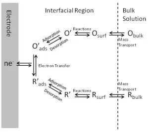
Page | 2
Figure 1-1: A schematic of the processes undergone in basic dynamic
electrochemistry
1.1.1 Electron transfer at the electrode
In an electrode material, which is usually metallic, the overlap of atomic
orbitals allows for electrons to move freely within the crystal lattice. These electrons
occupy a number of energy levels with a maximum state known as the Fermi level.
The position of the Fermi level can be tuned using an electric potential, either
increasing or decreasing the energy. Electron transfer from an electrode to a reactant
molecule only occurs if the Fermi level in the electrode material, is at a higher
energy than the lowest unoccupied molecular orbital (LUMO) of the electroactive
[image:32.595.154.454.68.335.2]Page | 3
Figure 1-2: Energy level diagram. In case a) there is insufficient energy to
reduce species, O, by tuning the Fermi level with an applied potential there is now
sufficient energy for electron transfer between the metal electrode and O to occur as
in case b).
For a system at equilibrium depicted in equation 1.1, the Nernst equation
(1.2), can be used to relate potential to the concentration of the molecule being
oxidised or reduced.2
O ne R 1.1
0' ln R
O
a RT
E E
nF a
1.2
ac 1.3
Where E is the potential at the electrode, E0’ is the standard electrode
potential, R is the molar gas constant, F is Faraday’s constant, n is the number of
electrons transferred determined form the stoichiometry of the reaction in equation
1.1, a is the activity of the species defined by the activity coefficient
and thePage | 4
None of the systems studied in dynamic electrochemistry are at equilibrium,
but in some instances electron transfer kinetics are so fast that the response will be
governed by mass transport. In this case it is reasonable to assume Nernstian
behaviour or reversible kinetics at the electrode surface.
When Nernstian behaviour no longer holds at the electrode and electron
transfer kinetics dominate, the simplest relationship is that defined by Butler and
Volmer and so the rate of the forward reaction kf and backward reaction kb are
defined in equations 1.5 and 1.6.
f b
k k
O ne R 1.4
0'
0exp( ( ))
f
nF E E
k k
RT
1.5
0' 0exp((1 ) ( ))
b
nF E E
k k
RT
1.6
where k0 is the standard rate constant, α is the electron transfer coefficient, with the
remaining variables being previously defined. The equations defined arise from
transition state theory and are used most in electrochemistry for the analysis of
electrode kinetics. Although more complex models are available they were not
considered in this work.2
1.1.2 Mass transfer
In the context of the work herein, mass transfer describes the motion of
species in solution, and particularly between bulk solution and an electrode surface.
Page | 5
motion of a portion of solution. Thus, the variants of mass transfer can be
categorised into diffusion, migration and convection. It is the combination of all
three processes which governs the overall mass transfer and can be described by the
Nernst-Planck equation.2
, , , i
i i d i m i c i i i i
z F
J J J J D C D C C v
RT
1.7
Ji,d , Ji,m and Ji,c denote the diffusive, migrative and convective components of the
flux of species i; Di represents the diffusion coefficient; Ci represents the
concentration; zi represents the charge on the species; ϕ represents the electric
potential; v is the velocity of the solution; T is the absolute temperature and the other
terms have been defined. Mass transfer will be described in more detail in the
following sections.
1.1.2.1 Diffusion
Diffusion occurs due to thermal movement of species in solution for both
charged and neutral species.1 The rate of net diffusion depends on the concentration profile at a specific location and can be described by Fick’s first 1.8 and second 1.9
laws.2
,
i d i
J D C 1.8
2 i i i C D C t
Page | 6
The first law describes the net flux in terms of a concentration gradient,
within a system, towards an electrode, considering the variation in concentration in a
specific location within a specific time. Equation 1.8 has a negative sign because
species move from a region of high concentration to regions with a lower one. The
second law merges the general conservation equation with the first law, which
describes the variation in concentration with time due to diffusion.1 This is the equation that is normally solved to predict the current at an electrode.
The driving force for diffusion of species within a solution is the gradient in
chemical potential of the species, Fick’s first law can be rearranged to yield and
describes the case where the species is electrically neutral:2
i i
i i
D C J
RT
1.10
ln
i i RT ai
1.11
where µi is the chemical potential of the species, µiα is the standard chemical
potential in phase α and all other variable have been previously defined. For charged
species the electrochemical potential is given as:
i i z Fi
1.12
Where i is the electrochemical potential and all other parameters have been
previously defined.2
Page | 7 1.1.2.2 Migration
Migration refers to the movement of charged species due to a potential
gradient exerted by an electric field existing at the electrode solution interface. This
exerts an electrostatic force on charged species within solution pushing ions towards
or away from the electrode. The migratory flux is described in equation 1.12 and is
dependent on ion mobility, concentration of the ion and the electric field.
i
m i i
z F
J D C
RT
1.12
The term i i
z F D
RT describes the mobility of the ion and is usually denoted as ui.
2
1.1.2.3 Convection
Convection occurs due to mechanical forces acting on the solution, causing
motion in the fluid. There are two types of convection: natural which arises, for
example, from thermal gradients within the solution and / or variations in density;
and forced which arises from stirring or pumping of the solution.1 The convective flux of a species, i, in solution is given by the equation:
,
i c i
J C v 1.13
1.1.3 Experimental electrochemistry
1.1.3.1 Macro electrodes
Macroelectrodes are ones which have dimensions from the millimetre to the
centimetre range. Due to its large size these electrodes experience planar diffusion
Page | 8
µAmp, they have to be used in a 3 electrode configuration where the counter
electrode compensates for Ohmic drop in solution.
Figure 1-3: a) shows the linear diffusion profile towards a macroelectrode
and b) shows a 3 electrode system where ref is the reference electrode and counter is
the counter electrode bathed in solution and connected to a potentiostat.
1.1.3.2 Cyclic Voltammetry
Cyclic voltammetry (CV) utilizes a potential scanned backed and forth between two preset potentials, E1 and E2 at a steady scan rate v / Vs-1. This gives a triangular waveform, shown in Figure 1-4:
Figure 1-4: A typical waveform for a CV broken up into segments. The cycle
Page | 9
Experiments are usually conducted in stationary solutions and hence rely on the diffusion of the reactants. This can be determined by Fick’s second law shown in equation 1.9, for a species i.
Cyclic voltammetry is the most widely used technique for the characterisation of redox systems1. It provides qualitative information about the number of oxidation states and their stability,1 also giving information about surface reaction mechanisms.
Figure 1-5: Initially the chemical reaction is governed by kinetics of the
heterogeneous electron transfer across the electrode / solution interface. At the
maximum the current response is due to diffusion.1
The shape of the voltammogram depends on the reversibility of the redox
couple, and/or the electrostatic repulsive or attractive forces between the redox
centres (the voltammogram described here is only valid for a macroelectrode). The
peaks in the voltammogram occur because mass transport cannot compete with
Page | 10 1.1.3.3 Amperometry
Amperometry is defined as the measurement an electrical current or a change in
electrical current, with an applied, fixed potential.2 In this case a fixed dc potential is applied to the working electrode, with respect to a reference electrode, and a net
current flows due the oxidation or reduction of an electroactive species. This
technique is commonly used in electrochemical titration methods and is described
elsewhere.2
1.1.3.4 Potentiometry
In a potentiometric experiment no net current flows, i.e. no electrochemical
(Faradaic) reaction occurs. The measured potential is usually dependent on the
thermodynamics of the system, but not always2 and is used to determine the concentration of an analyte in solution. This analytical method is the basis for ion
selective electrodes.2
1.2 Scanning Electrochemical Microscopy (SECM)
SECM is a completely different means of performing dynamic
electrochemistry.3 The technique is based on the utilization of a mobile ultramicroelectrode (UME), placed in close proximity to a surface, which can
provide quantitative information on interfacial physicochemical processes.3,4 A UME can be used either as a potentiostatic or potentiometric probe, to determine the
properties of a sample interface. The type of electrode used depends on the process
Page | 11
by electrolysis, the probe can be used to induce and monitor a specific interfacial
process, or simply to detect a particular species involved in an interfacial process.4-5 If the SECM measurement involves a non-invasive detection process, then
potentiometry also becomes a possibility, greatly extending the range of species and
processes that can be investigated.6 The use of a UME greatly improves the spatial resolution and implementation of electrochemical techniques, and allows for
investigation of activity and topography at an interface at a localized scale.4,7-9 Due to the dimensions of the UME (typically a disc electrode of 25 µm diameter or
smaller), it is also possible to minimize the influence of many sources of
experimental errors, namely, resistive potential drops in solution and charging
currents. This allows for scrutinous investigation of minute electrochemical
processes (with currents normally in the nA - pA range), such as ion exchange
reactions at polymer – electrolyte interfaces10-11 and immobilized enzymes.3,7,12-15 The investigation of biological samples is a common application for SECM, being
able to monitor activity4,12 also attempting to perform topographical imaging, which is a major challenge.7, 8 Figure 1-6 shows the information which can be extracted from amperometric UME used in SECM. The arrows represent the flux of
Page | 12
Figure 1-6:Schematic of the varied modes of application of SECM (top) and
the current response observed in each (bottom), as normalised by the current far
from the surface.
1.2.1 Instrumentation
The basic elements of an SECM setup are depicted in Figure 1-3 and will be
discussed in the following sections.
Page | 13 1.2.1.1 Ultramicroelectrodes (UMEs)
Several definitions of a UME are available such as: ‘an electrode which is
smaller than the scale of the diffusion layer in readily achievable experiments,16 and ‘experimentally a UME can be defined as an electrode having at least one dimension,
the critical dimension, less than 100 µm.16 In essence a UME is one which shows non – linear (edge) diffusion on the time scale of a typical voltammetric experiment,
which puts the length scale in the range identified in these definitions. Unlike
macroelectrodes UMEs are usually used in a 2 electrode arrangement (Figure 1-7)
due to the magnitudes of currents passed are usually on the nAmp range or less, in
this case Ohmic drop is considered negligible. In depth reviews on electrode design,
fabrication and characterization can be found elsewhere.16-17 The most common mode of preparation of a UME involves the thermal sealing of a metal wire in a glass
capillary, yielding a disc shaped electrode of typical diameter 0.6 µm to 100 µm
(refer to Figure 1-8 for UME images).
Figure 1-8: Optical microscope images of a UME from an end on view and
side view.16
The term RG defines the ratio of the surrounding insulator dimension to that
of the tip and is usually about 10. This ratio is chosen as it minimizes effects from
back diffusion enabling the response to be more sensitive to surface processes9. As
multi-Page | 14
dimensional diffusion, than linear diffusion (as experienced by macroelectrodes).
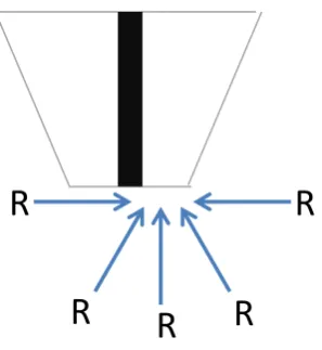
This also means that the diffusional flux at an UME is greater than that for larger
electrodes for equivalent conditions (e.g. scan rate).16 This feature can be attributed to the size and geometry of the electrode and the resulting diffusion pattern shown in
Figure 1-9.
Figure 1-9: Schematic of a hemispherical diffusion field established for the
steady state diffusion-limited oxidation of a bulk solution species.
1.2.1.2 Probe positioning
A key feature of SECM is that the electrode is connected to a piezoelectric
stage, allowing motion control in the x, y, and z directions.4 In many cases nanometer scale precision is possible depending on the type of piezoelectric
positioner used, similar to those used in scanning tunnelling microscopy (STM).18 For SECM, the greatest precision is required in positioning the z direction, i.e. in the
electrode approach to the surface. The piezoelectric positioners are typically
controlled by a high voltage amplifier receiving a signal from a control card
converting the signal via a digital to analogue converter. Initial positioning (lower
resolution) is often achieved via manual micrometer stages. A video microscope is
R
R
R
R
Page | 15
sometimes used, in order to facilitate tip approach, allowing the initial approach to
the surface to be achieved via the manual control.19-20
1.2.1.3 Signal generating / acquiring devices.
In most cases, the signal detected in SECM is a current. This is converted to a
voltage via a current to voltage converter and then amplified, with gain settings
calibrated to a specific range of values. For the investigation of unbiased surfaces
with SECM, a typical two electrode system (a working electrode and a reference
electrode) is sufficient to bias the tip to initiate an electrochemical process. In cases
where the surface also requires biasing externally, a bipotentiostat is used to control
the system. All signals are then acquired via a data acquisition card and processed in
specific host software, generating a visual depiction of interfacial processes.
1.2.2 Modes of operation
1.2.2.1 Feedback mode
The feedback mode is the main mode used in SECM and it includes detecting
a species by electrolysis at a diffusion limited rate. Figure 1-10 shows the variation
in electrochemical response with respect to the substrate. It must be noted that the
term feedback mode should not be confused with positional feedback as in
conventional scanned probe techniques as SECM, has no positional feedback. If the
UME is approaching an insulating surface, the diffusion of redox species towards the
active area of the microelectrode will be blocked by the surface. This means that the
hemispherical diffusion field established at the UME is distorted by the insulating
Page | 16
available for the conversion and hence the current measured at the microelectrode
drops.21 This phenomenon is known as ‘negative feedback’.
In the case of approaching a conducting substrate, the electroactive species
now encounters a surface whereby electron transfer may occur. In this mode, the tip
is held at a potential, initiating the diffusion-controlled electrolysis of a target species
in solution (this is also performed during negative feedback). This, in turn,
experiences positive diffusional feedback when positioned close to a conductor, due
to the substrate sometimes following Nernstian behaviour (in some cases it is
necessary to apply a bias to the electrode) , such that the direction of the tip electrode
reaction is reversed on its surface, thereby increasing the overall current measured.22 Essentially the equilibrium, disturbed by the SECM tip will tend towards being
re-established by the Nernst potential of the surface to re-convert the species converted
at the tip and will therefore increase the current at the tip since no depletion of
convertible species happens21. The same processes are undergone for any sample being investigated and a more detailed description can be found in literature.
4-5,10,12-14,23-24
Figure 1-10: A schematic of SECM operating in feedback mode when
Page | 17 1.2.2.2 Generator collector mode
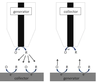
There are many other SECM operative modes among which generation /
collection modes4-5,25-26 are most prominent. In substrate generation – tip collection (SG-TC) one detects species emerging from a surface as a tip current and in tip
generation – substrate collection (TG-SC) a species is generated at the tip and
detected as a current at the surface (shown in Figure 1-11).4 For example, if electroactive species diffuse through a pore opening or from a sample surface, they
can be converted by the SECM tip if it is held at a suitable potential,4-5 determining the activity at that specific location, on the other hand species can be generated at the
tip and collected at the surface5. These methods are designed to compensate for the different effects observed in each case. Specific details of technique variations can
[image:47.595.159.486.417.700.2]be found elsewhere. 4-5
Page | 18
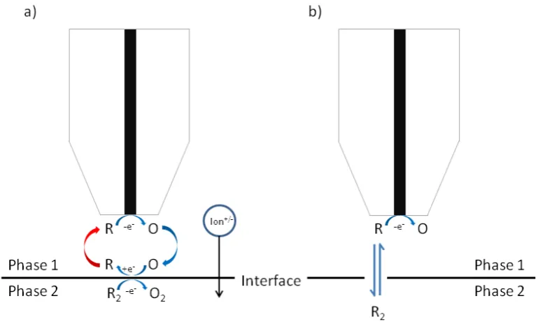
1.2.2.3 Permeability and ion transport at interfaces
SECM can be used to monitor or perturb interfacial processes by use of an
amperometric probe. In the general case the UME immersed in a liquid phase and is
in close proximity to a secondary phase, for example an immiscible liquid, gas or a
biological membrane, with the process being studied initially at equilibrium.20,27 A potential is applied to the probe oxidising the species in phase 1, driving the transfer
of reduced species in phase 2 across the interface. An enhancement in tip current is
observed and the reduced species reaches the tip via hindered diffusion through
phase 1. This response is governed by diffusion in the two phases and the interfacial
kinetics.20 Even though this method has been used mostly with metal electrodes, liquid-liquid voltammetric probes can also be used as a study of ion transfer across
interfaces. This method has proved useful in determining solute transfer across
biological membranes and bathing solution, as a non invasive method.27-29
Figure 1-12: Inducing an interfacial process using feedback mode a) monitoring
[image:48.595.127.512.452.684.2]Page | 19
1.2.2.4 Pipet based liquid / liquid interface probes
The tips used here comprise of pulled glass or quartz pipets and the tip
current is due to either facilitated30 or simple ion transfer31 across a liquid/liquid interface, in most cases an aqueous / organic (inside the pipet) interface.5 These pipets are usually polished.32 Due to the ease of preparation, compared to traditional SECM electrodes, pipets with radii less than 10 nm have been reported.33 Similar to negative feedback mode with traditional SECM electrodes, when over a solid
substrate ion transfer across the solution interface is hindered and leads to a decrease
in tip current.5 Enhancements in tip current indicate additional ion flux from the substrate and examples include ion transport measurements through porous silicon
membranes34 as well as the effects of silver ions in living cells.30 When compared to the response of traditional platinum electrode a similar response was obtained with a
liquid-liquid probe over a silicon wafer in constant current mode,31 indicating that this method can be very useful for high resolution electrochemical imaging and
kinetic experiments.5 This same method can also be used to deliver species to a substrate surface and has been used for metal ion electrodeposition35 and also to study the reactions of neutral species via facilitated ion transfer.36
1.2.3 The issue of substrate topography
In SECM, the probe needs to be positioned close to an interface with high
precision and although this is achievable using piezoelectric positioners, it is often
very difficult to determine the precise tip substrate separation. It is possible to use
the amperometric response of the tip electrode when approaching to an inert surface
Page | 20
studied and hence is not a viable solution. This has led to the development of hybrid
techniques in which various modes of operation attempt to solve this problem using
unique positioning methods. These techniques will be discussed briefly in the
following sections.
1.2.3.1 Scanning Electrochemical Microscopy – Atomic Force Microscopy (SECM-AFM)
One of the most well known hybrid techniques SECM – AFM combines both
techniques by integrating a UME into an AFM tip. AFM acquires high resolution
topographical images by monitoring interaction forces between the sharp tip and the
surface attached to a force sensitive cantilever.37 The merging of both techniques allows for the acquisition of topographically related, electrochemical activity at very
high spatial resolution.38 The most important component of this technique is the combined probe and significant progress has been undergone since the first reported
instance, which consisted of the fabrication of a platinum wire into a force sensitive
cantilever / electrochemical probe.39 Batch fabrication methods are now available with different designs of probes being produced, either having ring electrodes
embedded in a commercial AFM tip40-41 or with the apex also acting as the working electrode.42-44 Other methods of probe fabrication have also been reported, together with modelling of the tip response, but will not be discussed in this report.
Applications of SECM-AFM are wide due to the abundance of information
that can be gained from this method. Typical test substrates have included patterned
conducting-insulating samples and have been imaged in SECM feedback mode or
Page | 21
activity of electrode materials44,46-47 and localised corrosion processes.48-53 Membrane transport processes have also been investigated and are of great
importance in separation methods, membrane supported reactions, gas permeation
and in biological systems. Examples of systems studied include; fabricated polymer
membranes, whereby the transport of redox mediator through each pore was
investigated, correlating well with differences in pore diameter54 and transport of glucose through a polycarbonate membrane, with the tip functionalised with an
enzyme, glucose oxidase.55 The enzyme converted glucose to hydrogen peroxide, which could be detected electrochemically and the local concentration of glucose
corresponded with the predicted diffusion through each pore opening.55 SECM-AFM has also been used for electrochemical patterning, giving the ability not only to
generate smaller structures but also characterise them topographically.56-57
1.2.3.2 Scanning Electrochemical Microscopy – Scanning Tunnelling Microscopy (SECM-STM)
Electrochemical scanning tunnelling microscopy (EC-STM) allows for the
investigation of electrochemical reactions at sub Å to the nm level.58 The probe consists of a sharp STM tip coated with an insulating layer exposing only the end,
reducing any unwanted electrochemical processes to the tunnelling current. EC-STM
was subsequently combined with SECM using essentially the same setup. In this
technique the tunnelling current was used for tip positioning and tracking
topographical features. By implementing a consecutive lift mode, whereby the tip is
retracted by a user defined distance, electrochemical measurements, common in
Page | 22
stainless steel, where current spikes across the image were linked to pitting precursor
sites,59-60 electrochemical deposition of a palladium nanoparticle from the tip also studying its electrocatalytic activity,61 the study of the electroactivity of a gold electrode modified with a self -assembled monolayer and mechanically scratched,
observing an increased SECM feedback current at these specific sites62 and also the integration of a pH electrode into the tip investigating the property dependence of
electropolymerised polyaniline films.63
1.2.3.3 Dual mediator
Another approach for deconvoluting electrochemical activity and topography
is to use two different mediators, one of which will be inactive to the surface
chemistry being studied. By scanning over the substrate in a constant height mode,
the inert mediator can allow for topographical information to be gained. A
subsequent retrace at a potential at which the electrochemically active mediator to
the system being studied, identifies a particular property connected to the activity of
the sample. Some examples of this method have been seen in mapping the
permeability of molecules in biological systems.28-29
1.2.3.4 Shear force SECM
This method achieves control of tip substrate separation by using a probe
oscillated in the x-y plane, detecting the shear forces that occur when in close
proximity to the surface of interest, that result in a damping of the oscillation
Page | 23
scanning optical microscopy (NSOM).65 It was found that this effect had a significant distance dependence (particularly close to a surface) and was a
convenient way of controlling the position of the UME for constant distance
imaging. The damping in oscillation amplitude can be monitored in two ways: 1) by
shining a laser on the very end of the electrode and detecting the signal using a
photodiode64,66 2) by using a quartz crystal resonator attached to the probe and detecting the damping in vibration.67-68
Due to the mode of operation of this technique, the probes used need to be
sub micron, needle like UMEs, in order to achieve a sufficient amplitude of
oscillation and the topographical resolution is dependent on the tip diameter.69 This places some limitations on the types of processes that can be studied. This setup can
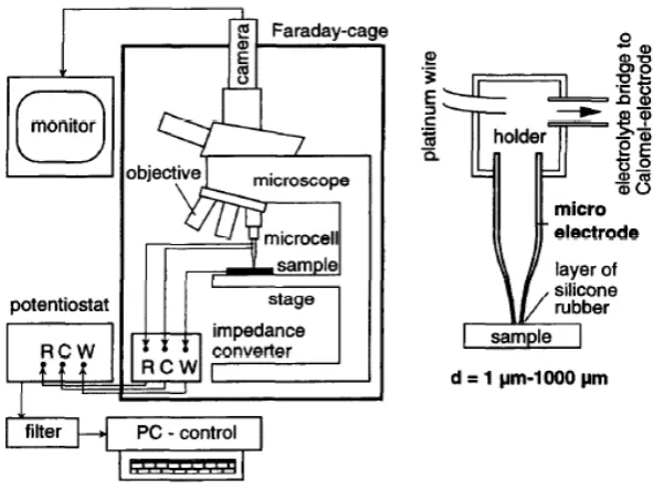
also be used with non pipet-based potentiometric probes66, with applications in crystal dissolution studies70, high resolution pH mapping71 and also metal deposition.72 The application of constant-distance shear-force SECM has allowed for the characterisation of single cells.4 By mounting the setup onto an inverted microscope, the terminology Bio-SECM was introduced. An alternative imaging
mode has also been developed and is termed 4D shear force constant distance
SECM.73 In this mode, the tip performs a series of approach curves at each point measuring the tip current at specific distance whilst approaching and also whilst
retracting by a user defined amount. In this method diffusion profiles can be obtained
and was demonstrated in generator-collector mode above a platinum band
Page | 24
1.2.3.5 Alternating Current Scanning Electrochemical Microscopy (AC-SECM)
AC-SECM utilises an alternating potential (ca.10 mV) superimposed on a
much larger tip bias that is generated from a function generator or internal oscillator
of a lock-in amplifier (LIA). The modulated current signal is recorded, exhibiting a
distance dependence between the tip and sample and hence can be used for
positioning and for constant distance imaging.74 This method does not require a redox mediator in solution, as it is the local impedance between tip and sample
which is measured.74 When a redox mediator is added, the Faradaic process can be used to determine the local electrochemical properties of the sample whilst the high
frequency impedance signal is used for tip positioning and can be easily separated
out. This method has been successfully used for a number of systems and an in depth
review has recently been published.74
1.2.3.6 Tip position modulation (TPM) - SECM
TPM was an early advancement on the traditional feedback mode in SECM.
In this configuration the amperometric tip is oscillated sinusoidally, perpendicular to
the surface, with a very small amplitude.75 The modulation in the tip position causes a modulation in the tip current at the same frequency, and through the use of lock-in
techniques this signal is detected. The modulated signal further reduces any
experimental complications which can arise due to potential drift and low signal to
noise ratio when using much smaller UMEs. Both the amplitude and phase of the
modulated current can be used to relate topographical features to electrochemical
ones. When over an insulating substrate the modulated current is in phase with the
Page | 25
The in-phase response over a conducting substrate can be easily modelled as a
derivative of the steady-state behaviour but more complex models are required for
the response over an insulating surface, as recently introduced by Edwards et al.76 This method has shown to have improved sensitivity over tip-substrate separation,
with minimal experimental modifications.75
1.2.3.7 Intermittent Contact SECM (IC-SECM)
Tip-substrate separation has commonly been controlled in AFM by
oscillating the tip at its resonant frequency and then monitoring the damping in the
oscillation amplitude resulting from surface contact.77-78 This concept was recently applied to SECM but oscillating the tip at much lower frequencies (ca. 70 Hz).79 In this mode, traditional SECM probes are utilised and, once the probe comes into
contact with the substrate, a constant damping in the amplitude is maintained
controlling the tip substrate separation. Once in contact, the topography,
electrochemical response and also the modulated electrochemical response (resulting
from the oscillating probe) are recorded. The technique utilises the fact that the tip
and substrate will rarely be perfectly aligned and so only a small portion of the glass
comes into contact. A lift mode was also introduced in which the tip is retracted on
the reverse line and the current response measured whilst following the topography
at a user-defined distance away. The method was proved on a gold band model