Analog Spiking Neuron with Charge-Coupled
Synapses
Yajie Chen
∗, Steve Hall
∗, Liam McDaid
†, Octavian Buiu
∗, and Peter Kelly
†Abstract—This paper presents a compact analog
neuron cell with an array of charge-coupled synapses connected via a common output terminal. Synaptic responses are fed into a current mirror, the summing point of the neuron. A couple of CMOS inverters are employed to implement the temporal and spatial in-tegration of weighted input spikes generated by the synaptic array. The decay of the membrane potential is mimicked by the charge leakage through a reverse-biased diode, whose model is verified by comparing the simulations and measured data. Spice simulation results show that the proposed neuron cell is capable of capturing the summing and thresholding dynamics of biological neurons.
Keywords: neuromorphic circuits, silicon synapse, spiking neuron
1
Introduction
In the effort to attain human-level intelligence in both hardware and software, a considerable amount of neu-ral network research has been performed where learn-ing algorithms, trainable networks, dedicated hardware and applications have all been developed throughout the past few decades. Recently experimental evidence has re-vealed that the traditional mean firing rate method could not describe brain activity since the reaction times are too short to allow temporal averaging for the calculation of the mean firing rate. This has given rise to the interest of alternative coding techniques which has led to the recent trend of Spiking Neural Networks (SNNs), an essential component in information processing by the brain [1]. Therefore much exciting research aimed at implementing human-level intelligence within networks of neurons has been proposed recently [2]-[4]. However these implemen-tations require complex circuitry and consequently the power dissipation of the neuron circuit could be a ma-jor problem especially for large network level. Achieving high neuron density and low power operation are major constraints in the development of silicon neural systems.
In this paper, we present a biologically plausible
neu-∗Department of Electrical Engineering & Electronics,
University of Liverpool, Liverpool L69 3GJ, UK (Email: [email protected]; [email protected]).
†School of Computing & Intelligent Systems, University of
Ul-ster, Londonderry, BT48 7JL, UK (Email: [email protected]).
ron cell based on our recently developed charge-coupled synapse [5]. This silicon synapse produces a weighted spike characteristic using a simple device and when em-bedded in a point neuron cell, a time dependent out-put is produced; the outout-put being referred to as the post-synaptic potential (PSP). The signals from charge-coupled synapses are integrated as the summed current by a current mirror configuration where an array of synapses can be connected via a common output node. The functionality of thresholding is realised by a CMOS inverter, which accumulates the weighted charges and captures the time dependency of the postsynaptic mem-brane decay.
2
The Charge-Coupled Synapse
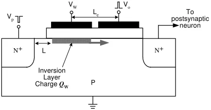
We now review our charge-coupled synapse which is ca-pable of mimicking the spiking dynamics of a biological synapse. Fig. 1 shows the n-channel, two-phase charge-coupled synapse, essentially consisting of two MOS ca-pacitors in series. For the present study, we consider that a voltage, representing the weight, is placed on the first capacitor, but the intention in due course, is to include a floating gate upon which charge can be stored in a sim-ilar manner to that of non-volatile memory. The second MOS capacitor serves as the input node of the synapse which is triggered by the pre-synaptic signal. This device mimics the exhibitory synapse. An inhibitory synapse could be implemented as a p-channel charge-coupled de-vice. The output is formed by an n-type implant, on the right hand side of Fig. 1. The n-implant to the left can be used as a minority carrier injector, to speed up the
non-Le To
postsynaptic neuron Vo
P
N+ VW
N+ L
Vp
[image:1.595.320.537.607.720.2]Inversion Layer Charge QW
S
pi
ki
ng
c
ur
re
nt
(A
)
Transient time (ns)
0 1 2 3 4 5 6 7 8
-4.0x10⁻⁷
0.0x100
4.0x10⁻⁷
8.0x10⁻⁷
1.2x10⁻⁶
[image:2.595.63.275.74.255.2]Vgate=1.0 V Vgate=0.8 V Vgate=0.6 V
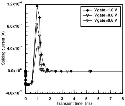
Figure 2: Spiking characteristics of the charge-coupled synapse.
equilibrium relaxation response of the device to achieve biological scale time regimes [6].
The synaptic weight is stored as the charge packetQWin the inversion layer of the first MOS capacitor. Note that the amount of charge increases linearly with the applied voltage on the first MOS capacitor which operates in the strong inversion state. Therefore the weight modification depends on the updating of the magnitude of the voltage VW; weight storage will be considered in a subsequent publication. At the instant that the pre-synaptic neu-ron sends out a spiking signal, the second MOS capacitor is driven into the deep depletion state, and the weight charge is released to the output terminal due to the lat-eral potential variation. Consequently the synapse com-putes the weighted signal as an output current as shown in Fig. 2. The majority of charge is transferred within a few nanoseconds, and the amplitude of the spiking cur-rent is proportional to VW. We use this relationship to implement synaptic plasticity.
3
The Spiking Neuron
In ideal spiking neurons if the sum of the inputs, from different dendrites, surpasses a particular threshold then a spike is produced which propagates along the axon to other synapses. The integrate-and-fire (I&F) neuron model consists of a capacitor and a threshold device [1]. Fundamentally the cell membrane acts as a capacitor where the potential of the cell membrane can be mod-eled as the response of a capacitor to an injection of cur-rent. In response to a stimulant current the capacitor is charged, and when the potential reaches level, a spike is produced and the potential subsequently returns to the resting potential. The concept presented here however, represents a new paradigm to realize a spiking neuron, which has the potential to build more biologically
plau-sible networks.
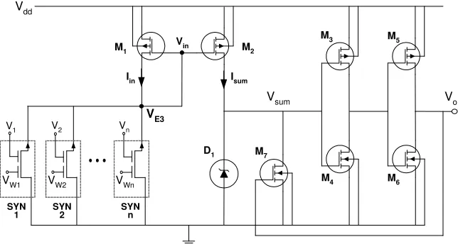
The circuit diagram of the proposed silicon neuron cell is shown in Fig. 3. M1-M2 constitutes a current mirror which is used to integrate the weighted current spikes from a number of n-type charge-coupled synapses. M3 -M4forms a CMOS inverter that thresholds the summed signals and generates an output hi-lo transition indicating that the neuron has fired. A ’leaky’ diode D1 enables charge leakage that effectively mimics the PSP decay of biological neurons. M7 is controlled by the feedback of the neuron output of the second CMOS inverterM5-M6, and serves to reset the neuron cell after firing. The second CMOS inverter gives a lo-hi transition and is the actual output which is fed to subsequent synapses.
The charge-coupled synapses are directly connected to the drain ofM1via a common output terminal. Note that the leakage of charge through the p-n junction formed by the output terminal and the substrate in the silicon synapse is controlled by the thermal generation lifetime and this process is orders of magnitude greater than the aforementioned charge transfer time. Therefore we can consider that no charge is lost during the summing oper-ation. A refractory period is present after the integration of the spiking currents because the recovery of the silicon synapses from the deep depletion conditions takes the or-der of milliseconds when we employ lifetime quenching. Note that a pulse Vp applied to the left hand n+ region
of Fig. 1, causes injection of minority carrier electrons to facilitate and control this relaxation process.
3.1
Current Mirror Operation
All n synaptic output signals are integrated onto the drain of M1. The transfer of weighted charge packets
in n-connected silicon synapses results in a current Iin.
Two p-channel devices which can be triggered byIinare
required in the current mirror configuration. Therefore the accumulated charge is transferred to the drain ofM1, the reference currentIinincreases and is mirrored asIsum
in M2. The current Isum charges the gate voltageVsum
of the first CMOS inverter and D1 is now under reverse bias.
Assume that two p-channel MOSFETs,M1andM2, have the same oxide thickness and threshold voltage. The cur-rent forM1 (assuming a long channel device) in satura-tion, whose source and substrate is connected to Vdd, is
given by:
Iin=k1
(VGS−VT)
2
2 (1)
wherek1=µCoxWL11 is the gain factor ofM1, andVGS =
Vin−Vdd.
The summed current from the synaptic array sets theVin
to:
Vin=VT +Vdd−
r
2Iin
k1
V1
SYN 1
Vn
SYN n
V2
SYN 2 Vdd
M1
Vsum
M2
M3
M4
M7
M5
M6
Vo
VWn VW2
VW1
VE3
Iin
Vin
Isum
[image:3.595.138.460.75.247.2]D1
Figure 3: The analog neuron circuit with an array of n-type charge-coupled synapse; The integration and thresholding functions are implemented by the current mirror configuration and CMOS inverter respectively.
By using appropriate W1/L1 ratio, larger fan-in of the current mirror can be achieved, allowing the integration of a large number of synapses. For the device with equal W1 and L1, 20 nm oxide, and the power supply of 3 V, the approximated number of synapses in one-dimensional array can be 320. M2 is then controlled byVin, and the
output currentIsum is obtained:
Isum=k2
(Vin−Vdd−VT)
2
2 (3)
wherek2=µCoxWL22 is the gain factor ofM2.
Substitute (2) into (3), the current Isum is expressed as
a function ofIin:
Isum=αIin (4)
where α=W2L1
W1L2 is the aspect ratio. This allows current
signals to have a fan-out greater than one and each out-put can be scaled using appropriate W/L ratios. If M1 and M2 are matched in all respects, Iin=Isum. After
the spike emission period,Vinis driven back toVdd
caus-ing the resettcaus-ing of the common output terminal of the synaptic array.
3.2
Thresholding Operation
The CMOS configuration is employed in the circuit to perform the thresholding function which plays an impor-tant role in neuron computation. The summed current Isum will charge the gates of M3-M4, causing the mem-brane voltageVsum to increase. Consider the case where
only one synapse is activated, and assuming a charing duration of τr. Therefore the membrane voltage can be
expressed as:
Vsum=
1
CON
τr Z
0
Iindt (5)
whereCON=CD+Cpis the capacitance at the membrane
node;CDis the diode capacitance;Cpis the capacitance
associated with the CMOS input gates.
The discharging of the gates ofM3-M4is due to the leak-age through the reverse-biased diode D1, as shown in Fig. 3. A ’leaky’ diode with a reverse-current characteris-tic dominated by Zener tunneling is preferred and results in biological scale relaxation rates. A numerical solution gives us the approximation that τr<<t(Vsum) [6].
The switching thresholdVT hfor CMOS inverter is defined
at the point where the input and output voltages are equal. Assume the voltage supply is high enough so that the transistors operate in saturation. The expression for VT his given by:
VT h=
(VT4−VDSAT2 4) +r(Vdd+VT3+VDSAT2 3)
1 +r (6)
where VT3 and VT4 are the threshold voltage of pMOS-FET and nMOSpMOS-FET; VDSAT3 and VDSAT4 are the sat-uration drain voltages for M3 and M4 respectively;
r=k3VDSAT3
k4VDSAT4 assuming equal oxide thickness; k3 and k4
are the gain factors.
WhenIin increases sufficiently to makeVsum exceed the
switching threshold of the CMOS inverter,M3is on and in saturation andM4 operates in the linear region. The output voltage is then located at low level, which means the neuron has fired. Subsequently the output voltage Vo of the neuron will increase rapidly and turn on the
transistor M7. This discharging action resets the inputs ofM3-M4, and the output Vois constrained by the
feed-back to be a very short voltage spike.
4
Results and Discussion
process. The oxide thickness of the accompanying tran-sistors is set to 20 nm which is used for charge-coupled synapse to provide enough fringing field. The threshold voltages of the p- and n-channel transistors are -0.74 V and 0.74 V respectively. For all the transistors, the same width and length are used (W=L=1.2µm). Note that the size of the transistors can be varied to demonstrate the exact behavior of the realistic biological neurons. We represent the output of the charge-coupled synapses us-ing current pluses of amplitude 1.2µA for each activated synapse. The power supplyVdd is set to 3 V.
A low breakdown ’leaky’ zener diode, whose reverse leak-age is dominated by Zener tunneling, is employed to form a leakage path. This allows the discharge of the PSP which mimics the decaying of the membrane potential in biological neurons. Fig. 4 shows the I-V curves of the zener diode under non-zener condition. Good correlation between the modeled and measured characteristic is evi-dent.
Voltage (V)
0 1 2 3 4
C
ur
re
nt
(A
)
Measured Modeled
Figure 4: Measured and modeled I-V curves of the reverse-biased zener diode with breakdown voltage of 4.7 V.
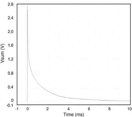
In our experiment, 100 synapses were activated concur-rently and the accumulated peak in current is 120µA. The membrane node voltageVsumat the gates ofM3-M4
is shown in Fig. 5. The voltage, following the rise of the synaptic signal, has a fast rise time reaching a peak value 2.7 V which causes the first CMOS inverter to change state as shown in Fig. 6(b), demonstrating the firing of the biological neuron. Due to the leakage ofD1, the PSP shown has a much slower fall time of the order of mil-liseconds, exhibiting the characteristic shape observed in biological neurons.
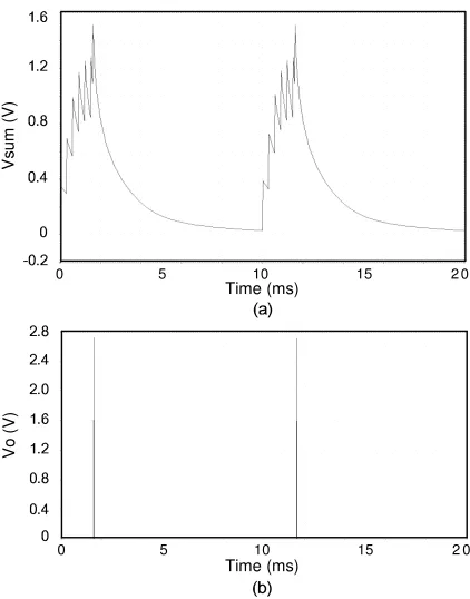
Fig. 6(a) shows the accumulation of successive PSP sig-nals when the synapses emit spikes with various time lags. In this simulation, there are 30 active synapses divided into 6 groups where each synapse is activated at the same
Time (ms)
V
su
m
(V
)
[image:4.595.323.534.71.258.2]-1 0 2 4 6 8 10
Figure 5: The membrane potentialVsumwhen the spikes
are generated at the same time.
time with an interval between each group. The associ-ated accumulation of charge produces theVsum shown in
Fig. 6(a). Therefore, the threshold is reached and the CMOS inverter is triggered to send out a spike, as shown in Fig. 6(b). Because the membrane node discharging is of the order milliseconds, the accumulation behavior is limited by the interval between each group. If we as-sume 2 ms interval, the majority of charges are used to compensate the leakage rather than commit to neuron’s firing. In addition, any spike arriving after the resetting of the membrane node will contribute to the subsequent firing events. It is worth noting that the resetting signal to the gate of M7 should have a certain delay to ensure the neuron output Vo has a fan-out capable of driving
multiple synapses on subsequent layers.
5
Conclusion
[image:4.595.65.277.318.501.2]Time (ms)
0 5 10 15 2 0
V
o
(V
)
"!
0 5 10 15 2 0 Time (ms)
#
V
su
m
(V
)
$%!
Figure 6: (a) The membrane potentialVsumwhen a series
of spikes are generated with various time lags; (b) The output voltage of the second CMOS inverterM5-M6. The neuron fires when the membrane potential exceeds the threshold of CMOS inverter.
References
[1] Gerstner, W., Kistler, W.M., Spiking Neuron Mod-els: Single Neurons, Populations, Plasticity, Cam-bridge University Press, 2002.
[2] Liu, S.C., Douglas, R., “Temporal Coding in a sil-icon network of integrate-and-fire neurons,” IEEE Transactions on Neural Networks, V15, N5, pp. 1305-1314, 2004.
[3] Bofill-i-Petit, A., Murray, A.F., “Synchrony detec-tion and amplificadetec-tion by silicon neurons with STDP synapses,”IEEE Transactions on Neural Networks, V15, N5, pp. 1296-1304, 2004.
[4] Indiveri, G., Chicca, E., Douglas, R., “A VLSI array of low-power spiking neurons and bistable synapses with spike-timing dependent plasticity,” IEEE Transactions on Neural Networks, V17, N1, pp. 211-221, 2006.
[5] Chen, Y., Hall, S., McDaid, L., Buiu, O., Kelly, P., “On the design of a low power compact spiking neu-ron cell based on charge-coupled synapses,” IEEE International Joint Conference on Neural Networks, Canada, pp. 1511-1517, 2006.
[6] McDaid, L., Hall, S., Chen, Y., Buiu, O., Kelly, P., “A biologically plausible spiking neuron cell in
[image:5.595.65.276.70.339.2]