Micro-structural and functional properties of TiAlCN/VCN
coating produced by High Power Impulse Magnetron
Sputtering Technology.
KAMATH, Ganesh K.
Available from Sheffield Hallam University Research Archive (SHURA) at:
http://shura.shu.ac.uk/20171/
This document is the author deposited version. You are advised to consult the publisher's version if you wish to cite from it.
Published version
KAMATH, Ganesh K. (2011). Micro-structural and functional properties of TiAlCN/VCN coating produced by High Power Impulse Magnetron Sputtering Technology. Doctoral, Sheffield Hallam University (United Kingdom)..
Copyright and re-use policy
See http://shura.shu.ac.uk/information.html
Acisetis Centre, City Campus Sheffield S1 1WD
1 0 2 0 0 6 8 4 6 9
Sheffield Haliam University
I Learning and information Services | Adsetts Centre, City Campus
Sheffield S1 1WD
I
ProQuest Number: 10700006
All rights reserved INFORMATION TO ALL USERS
The quality of this reproduction is dependent upon the quality of the copy submitted. In the unlikely event that the author did not send a com plete manuscript and there are missing pages, these will be noted. Also, if material had to be removed,
a note will indicate the deletion.
uest
ProQuest 10700006
Published by ProQuest LLC(2017). Copyright of the Dissertation is held by the Author.
All rights reserved.
This work is protected against unauthorized copying under Title 17, United States C ode Microform Edition © ProQuest LLC.
ProQuest LLC.
789 East Eisenhower Parkway P.O. Box 1346
Micro-structural and functional properties of TiAlCN/VCN
coating produced by High Power Impulse Magnetron Sputtering
Technology
Ganesh Kamath K
(Dedicated to my dear parents and brothers Jayesh and Radhesh)
A thesis submitted for the degree of
Doctor of Philosophy
in Materials Engineering and Research Institute,
Sheffield
I2KI
Hallam University
Declaration
The work reported in this thesis is original and was carried out by me under the supervision my Ph.D director Prof. Papken Eh Hovsepian and supervisor Prof. Arutiun P Ehiasarian, during my tenure as a Ph.D student at Nanotechnology Centre for PVD research lab, Materials Engineering and Research Institute, Sheffield Hallam University, UK. Thus the work carried out and explained in this particular thesis will not form basis for any other degree, diploma, associateship, membership or similar title of any university or institution.
(Ganesh Kamath) November 2011
NanoTechnology Centre
for PVD Research
Materials Engineering and Research Institute Sheffield Hallam University
ABSTRACT
Nanoscale TiAlCN/VCN multilayer coating was deposited in an industrial size 1000x4 Hauzer Techno Coating machine capable to operate with both unbalanced magnetron sputtering (UBMS) and high power impulse magnetron sputtering (HIPIMS) mode. The work was directed to study the impact of HIPIMS on the microstructure of the nanoscale TiAlCN/VCN coating, in relation to its properties at both room and elevated temperatures.
TiAlCN/VCN coatings were deposited by three different ways in combination of reactive UBM and HIPIMS technique. These are (i) reactive pure UBMS, (ii) reactive combined UBMS and HIPIMS, (iii) reactive pure HIPIMS. The microstructure and mechanical properties of the nanoscale TiAlCN/VCN coatings deposited in all the above combination of deposition have been studied. In all three cases, coatings were deposited in three major steps: (a) HIPIMS etching by Ar+ + V+ ions (b) a 300 nm thick TiAIN base layer deposition in Ar + N2 atmosphere followed by 2.5 pm thick
TiAlCN/VCN coating deposition in mixed Ar+N2+CH4 reactive atmosphere. PVD
chamber furnished with two pairs of opposing magnetrons with TiAl and V targets were utilised deposit this coating. During the second case of combined deposition, two opposing magnetrons were enabled to operate in HIPIMS mode and other two magnetrons were operated in UBMS mode, where as in third case only two opposing targets with HIPIMS power supply were utilised to deposit the TiAlCN/VCN coating respectively. In all the three cases, deposition parameters such as bias voltage (Ub = - 75V), deposition temperature (Ts = 450 °C) and total pressure of reactive gas mixture (Ar+N2+CH4; P = 4 X 10- 3 mbar) were maintained at similar conditions.
HIPIMS case, production rate of metal ions were appeared to gradually reduce at the expense of more free carbon production. XTEM analysis of pure HIPIMS deposited coating revealed the formation of three zones with different nanostructures across the film thickness. In the initial stages of deposition a TiAlCN/VCN nanoscale multilayer structure was formed (first zone) followed by a nanocomposite structure comprising TiAlCN/VCN crystalline grains surrounded by a carbon rich tissue phase (second zone). The grain size of the crystalline phase gradually decreased with thickness from diameter of 10-15 nm to complete dissolution in the third zone where Me- carbon with XRD amorphous structure was formed. In dynamic oxidation conditions, thermogravimetric analysis determined the temperature of the onset of rapid oxidation to be 800 °C for pure HIPIMS deposited coating. Compared to UBM and HIPIMS-UBM deposited TiAlCN/VCN coating, the oxide mass gain of the HIPIMS coatings was less than 30- 50%. A dry sliding wear tests were conducted at room temperature and different elevated temperatures of 200°C, 450°C, and 650°C on coatings deposited by all three cases. The friction coefficient was found to be p= 0.45 at room temperature, where the coefficient steadily decreased from 0.7 at 200°C, to 0.5 at 450°C and 0.4 at 650°C respectively. The scanning electron microscope and X-ray diffraction studies of the oxidised surface of the UBM and HIPIMS-UB deposited coating has revealed the formation of lubricant Magneli phase oxides of V2O5 and UO2 at elevated temperature.
The wear coefficient of the coating deposited by (HIPIMS-UBM) has shown two orders of magnitude lower value than that for the UBM deposited coatings, which represents significant advantage for coatings deposited by UBM. The wear coefficient in case of HIPIMS deposited coating reduces by one order of magnitude with the wear depth, with initial value of Kc = 3.8 x 10‘15 n^N 'W ^fter 500 laps to IQ = 4.4 x 10‘16 ir^N 'W ^fter
10000 laps. In comparison, UBM deposited TiAlCN/VCN coatings tested under similar conditions show an order of magnitude higher wear coefficient of 4.1 x 10‘15 n^N^m' 1
ACKNOWLEDGEMENTS
My sincere thanks to Prof. Papken Eh. Hovsepian for his valuable directions and guidance given during my stay at nanotechnology centre for PVD research (NTCPVD) lab. He is an inspiring guide and counsel. I admire his craving perfection and unquestionable ability of logical thinking. I truly enjoyed every bit of interaction I had with him, during my stay at NTCPVD research lab. Dear Professor, thank you very much for all the support and help I received.
I shall also very grateful to Prof. Arutiun P Ehiasarian for his constant support and guidance; supervision and encouragement; which helped me in giving a shape to this work. The credit for my early journal publications in IEEE transaction on plasma science and SVC 2010 Techkon proceedings; a full part of which is a content of my initial thesis, should go to him for his persistent push and guidance. I truly thank him for being very kind and supportive throughout my stay at NTCPVD.
I am indebted to Dr. Yashodhan Purandare, senior research fellow at NTCPVD, for his useful discussion during my early tenure of Ph.D work. His constant assistance during the deposition of multilayer thin films in industrial sized coating machine and handling of other laboratory scale instruments, were much valuable. I am very much thankful to Mr. Garry Robinson, principal technician at NTCPVD, whose quick help in terms of solutions to the technical problems faced during the Ph.D work made me to finish my Ph.D experimental work on time.
I deeply thank our collaborator Prof. Ivan Petrov and his colleagues at Fedric sietze materials research lab, University of Chicago, USA, for their outstanding help in high resolution Transmission Electron Microscopic and related work, which contributed a high quality result to my thesis. The endeavour of Mr. Stuart Creasy and Mr. Vinay Patel, Scanning Electron Microscope (SEM) experts at Materials Engineering and Research Institute, Sheffield Hallam University are gratefully acknowledged as well, for their true support for my SEM related work of present thesis.
Materials Engineering and Research Institute (MERI) at Sheffield Hallam University is greatly acknowledged for providing the financial support by way of fellowships to carry out this work. The director of MERI, both the present and past, are acknowledged for providing required facility. Office staffs at MERI, especially, Mrs. Indira, Mrs Gelian, Mrs Rachael, Mrs Jane, Miss Corrie, were also very helpful at times of need. They deserve to be thanked for their co-operation. Prior to my Ph.D work, I was doing my research at Crystal growth lab, Department of Physics, Indian Institute of Science, Bangalore India, where I had got the opportunity to start my research career in materials physics. I am very happy and would like to grately acknowledge Prof. H.L.Bhat and Dr. J.N.Babu Reddy (then Ph.D student of the department) for their supportive guidance. If not for this opportunity, I would not have got in to the field of research. I learnt many basics about research in that short period, while working on the non linear single crystal growth and their physical and optical properties. Interacting with the then Crystal growth lab members, viz. Dr. Vinayak (prl), Dr. Vanishri, Ganesan, Hari, and Naveen was illuminating. I am thankful to GOD for giving me an opportunity to get associated with my best friends Dr. Vinayak, Mohan, Prathap, Dr. Nonappa, Dr. Venkatesh, Dr. Anantheshwara, the Ph.D students from IISc, who encouraged me to continue research career.
I am fortunate to have met many nice people in MERI, who made my research life rich with pleasant memories. I shared many exciting moments with MERI research students Dr. Ante Hecimovic, Prakash muthudoss, Khairudhin, Dr. Mousa, Dr. Salaha, Daniel, Arun, Steve Dodds, Sampan, Itai Vutabwarova, Vikas. I certainly miss the light moments in beautiful Sheffield pubs, where I used to go out on some weekends with Harry (my supervisor), Yash, Daniel, Arun. I should not forget my B.Sc mentor Prof. K.G.Rathnakar and Prof. M.S.Adiga who taught me Physics and Maths respectively. I shall thankful to them.
Also, Prakash, Padmashree (sister) and Rajesh are my best friends with whom I spent my almost three years in UK. I miss them a lot in coming days.
Certification and conference attended during PhD
• Transmission electron microscopy for nanostructured materials, theory and practical training inTEM imaging; at Sorby nanocenter, University of Sheffield
• Sputter Deposition for industries advanced course given by Prof. Joe Greene, D.B .Willett professor from University of Illinois, Chicago,US A,
• Micro-structural Evolution during Thin Film growth, course by Prof. Joe Greene
D.B.Willett professor of materials Science, From University of Illinois, USA.
• Fundamentals of HIPIMS, course given by Prof. Amtiun Ehiasarian, NTCPVD, Sheffield Hallam Unviersity, UK, and Prof. Andre Anders, Lawrence berkeley.
• 1st International HIPIMS conference, Sheffield Hallam University, Sheffield, United Kingdom, (2009) : Presented Poster “Structural and High temperature tribological studies on HIPIMS/UBM deposited TiAlCN/VCN nanoscale multilayer coating”, G.Kamath, A.P.Ehisarian, P.Eh.Hovsepian
• Electron microscopy and Analysis group conference, University of Sheffield, Sheffield, United Kingdom. Presented Poster: “Microstructural and Raman spectroscopy of worn surface generated on TiAlCN/VCN at room and elevated temperature”, G.Kamath, A.P.Ehiasarian, P.Eh.Hovsepian
• 2nd International HIPIMS conference, Sheffield Hallam University, Sheffield, United Kingdom, (2010) : Presented Oral “Micro-Structural and Oxidative Mechanical Wear studies of TiAlCN/VCN Nanostructured Multilayer Coating Deposited by HIPIMS/HIPIMS-UBM Technique, G.Kamath, A.P.Ehiasarian, P.Eh.Hovsepian.
• 53rd Annual Technical Conference of Society of Vacuum Coaters, Orlando, April 17- 22 Florida, (FL), United States (2010).
• 12th International Conference on Plasma Surface Engineering, “Structure evolution in TiAlCN/VCN nanoscale multilayer coatings deposited by reactive High Power Impulse Magnetron Sputtering technology”, Papken Hovsepian, A. Ehiasarian, G. Kamath, Rick Haasch, Ivan Petrov.
List publications
Journal publications
• Tribological and Oxidation Behavior of TiAlCN/VCN Nanoscale
Multilayer Coating Deposited by the Combined HIPIMS/(HIPIMS-
UBM) technique, G. Kamath, A. P. Ehiasarian, Y. Purandare, P. Eh.
Hovsepian, Surface Coatings and Technology, 205, (2011),
2823-2829.
• Microstructure, Oxidation and Tribological Properties of
TiAlCN/VCN Coatings Deposited by Reactive HIPIMS, Submitted
for publication in J.Vac.Sci.Tech.A, P. Eh. Hovsepian, A. P.
Ehiasarian, G. Kamath, R.Haasch, I. Petrov, 2011.
• Properties of TiAlCN/VCN Nanoscale Multilayer Coatings
Deposited by Mixed High Power Impulse Magnetron Sputtering and
Unbalanced Magnetron UBM) Processes-Impact of HIPIMS during
coating, G. Kamath, A. P. Ehiasarian, P. Eh. Hovsepian, IEEE
transaction on plasma science (special issue), 38, No. 11, 2010, 3062.
Conference papers
• Micro-structural, Oxidation and Tribological Properties of
TiAlCN/VCN coatings deposited by Reactive HIPIMS, G. Kamath,
P. Eh. Hovsepian, A. Ph. Ehiasarian and I. Petrov, 54th Annual
Technical Conference of Society of Vacuum Coaters, Chicago, April
16-22, Chicago, United States (2011).
Table of Contents
Abstract... Ill Acknowledgments... V Certification and conference attended during PhD...VIII List publications...IX Journal publications... IX Table of Contents... X
CHAPTER 1 ...1
Introduction...1
1.1. Motivation...1
1.2 Purpose of present research work...3
1.3 Methods of approach...6
1.4 Structure of thesis...8
CHAPTER 2 ...9
Literature Review... 9
2.1 Physical Vapour Deposition Coating Technology (PVD)... 9
2.1.1 Fundamentals of Plasma...10
2.1.2 Plasma Discharge... 16
2.1.3 Sputtering... 20
2.1.4 DC Magnetron Sputter deposition technique...23
2.1.5 Cathodic Arc deposition...25
2.1.6 Unbalanced Magnetron Sputtering...27
2.1.7 High Power Impulse Magnetron Sputtering (HIPIMS)... 29
2.2 Thin film microstructural evolution...34
2.3 Nanostructured coatings...40
2.4 Nanostructured and composite coatings- for advanced Tribological applications ... 44
2.4.1 Nanostructured carbon films... 45
2.4.2 Advanced deposition systems for nanostructured and carbon based films ...48
CHAPTER 3 ...52
Experimental Methodology...52
3.1.1 Substrate material and specimen preparation techniques followed prior to
nanoscale TiAlCN/VCN deposition...52
3.2 Deposition Process and system geometry... 54
3.2.1 Reactive pure UBM and HIPIMS-UBM technology... 54
3.3 Coating characterising techniques...59
3.3.1 Adhesion test... 59
3.3.2 Rockwell C (HRc) Indentation method... 60
3.3.3 Pin-on-disc test... 61
3.3.4 Nano-hardness test...63
3.4 Plasma characterisation...64
3.4.1 Energy resolved mass spectrometry...64
3.4.2 Time averaged mode...6 6 3.5 X-ray diffraction (XRD)...6 8 3.5.1 Glancing angle geometry (GAXRD)...69
3.5.2 Bragg-Brentano (0/20) geometry...70
3.6 Raman spectroscopic analysis... 71
3.7 Thermo gravimetric Analysis... 73
3.7.1 Operating Principle...74
3.8 Scanning electron microscope (SEM)...75
3.8.1 Secondary electron and back scattered electron image... 76
3.9 Transmission Electron Microscopy (TEM)... 79
3.9.1 TEM Sample preparation...82
3.10 Dry high-speed milling test...82
CHAPTER 4 ...84
Results... 84
4.1 Plasma compositional analysis during TiAlCN/VCN deposition...84
4.1.1. Metal ion-to-gas ion ratio during HIPIMS etching...85
4.1.2 Metal ion-to-gas ion ratio during deposition of TiAlCN and VCN by UBM 8 8 4.2 Mechanical and tribological properties...93
4.2.1 Adhesion scratch and Rockwell-C indentation test...94
4.2.2 Tribological test... 97
4.2.3 Nanohardness measurements...103
4.3 Structure and microstructure analysis... 104
4.3.2 Raman Spectroscopy analysis... 107
4.4 Microstructural analysis...110
4.4.1 Scanning electron microscope analysis...110
4.4.2 Transmission electron microscope analysis... 113
4.4.3 Electron diffraction X-ray Analysis (SAED)... 117
4.5 Oxidation analysis...119
4.5.1 Thermo gravimetric analysis... 120
4.5.2 Phase composition and microstructure of the oxide scale on TiAlCN/VCN films deposited by mixed HIPIMS-UBM techniques 120 4.5.3 Morphology of worn surface after sliding friction...127
4.5.4 Raman analysis of worn surface... 130
4.6 Machining performance of TiAlCN/V CN coating deposited by combined HIPIMS-UBM technique... 131
4.6.1.... Raman spectroscopy investigation of the worn tool-work piece material surface...133
(A) Analysis of tool cutter coated with TiAlCN/VCN by UBM and HIPIMS-UBM technique... 133
CHAPTER 5 ...136
DISCUSSION...136
5.1 HIPIMS and UBM plasma-a comparison in terms of ionic composition 136 5.1.1 V+ + Ar+ ion etching by HIPIMS...136
5.1.2 Plasma composition during the deposition of TiAlCN/V CN coating 138 5.2 Mechanical and Tribological Properties of nanoscale TiAlCN/VCN coating 141 5.2.1 Mechanical properties determined for UBM and HIPIMS-UBM deposited coating...141
5.2.2. Room temperature friction and wear behaviour for UBM and HIPIMS- 143 UBM deposition case...143
5.2.3 Room temperature friction and wear behaviour for pure HIPIMS deposited case... 146
5.2.4 Friction and wear behaviour at elevated temperature...149
5.3 Microstructural analysis of TiAlCN/V CN coating - Impact of HIPIMS 151 5.3.1 X-ray diffraction and SEM cross sectional analysis of nanoscale TiAlCN/VCN deposited by UBM and HIPIMS-UBM technique... 151
5.3.2 Raman Spectroscopy... 153
5.3.4 Glancing angle X-ray diffraction analysis of reactive pure HIPIMS
deposited TiAlCN/VCN coating...156
5.3.5 Microstructural evolution of nanostructured TiAlCN/VCN coating - TEM study... 157
A. Reactive pure UBM and mixed HIPIMS-UBM deposited case 157 B. Reactive pure HIPIMS deposited case... 161
5.4 Oxidation behaviour...163
5.5 Wear mechanism and cutting performance of TiAlCN/VCN coated cutter in machining Al-alloy...168
Chapter 6 ...172
Conclusions...172
CHAPTER 1
Introduction
1.1. Motivation
Advanced fast growing industries like automotive and aerospace are facing the challenging problems of high speed cutting (HSC) and forming of soft and metallurgical aggressive materials such as Ti-, A1-, and Ni- based alloys [1]. During HSC machining operations, huge amount of heat is generated (with temperatures exceeding 700°C), which accumulates at the cutting edge. Since the above mentioned soft alloys have poor thermal conductivity and poor transfer of heat to the outgoing chip (especially Ti and Ti- based alloys), the counterpart should possess good thermal conductivity to dissipate heat away from the contact area of the cutting edge. One solution to this problem is the use of advanced tool protective coatings deposited by PVD methods. The overarching challenges in the current PVD technology is also to provide nanostructured multilayer coatings suitable for machining of above mentioned “sticky” alloys [1]. Essential requirements for successful tool coatings are high density, smooth surface morphology, high adhesion, and high wear resistance at cutting temperatures, low friction, good oxidation resistance, chemical stability and inertness relative to the work piece [2].
The early generation transition metal containing Nitrides, Carbides and Carbo-Nitride based monolayer coatings (TiN, CrN, TiCN,) were used substantially in machining carbon and alloy steels [3]. These coatings have been successfully developed by both CVD and PVD technology. But in the later stages of the research studies reveals that PVD technology was preferred over CVD technique to deposit coatings protecting the tools. The reasons are as follows [4]:
tribo-oxidation) which in turn shortened its life time and restricted its use at elevated temperature range [5]. Although, TiAIN coatings provide efficient protection against tribo-oxidation and wear at 700°C -850°C range when machining various steels, the higher friction coefficient value (p~0.85) has paved the way to explore more suitable coatings especially when machining of softer alloys is concerned. The reasons are the formation of huge build-up-edge (BUE) due to diffusion reaction with the work piece material, rough surface and high coefficient of friction against the ceramic nitride coatings [6]. Confronting
these situations, compositionally modified Ti-Al-C-N based coatings, metal- carbon containing nanocomposite coating and DLC (Cr/WC/a-CH) coatings have been introduced which have shown a considerable success in the market for the machining of these "sticky" alloys. Particularly the highly inert DLC coating have shown reduced BUE formation, however, due to adhesion problems, their life time is still insufficient [1]. Over-stoichiometric carbon based nanocrystalline/amorphous structured coatings (TiC/a-C) have also found their importance in low friction and wear resistance applications [7], but their poor thermal and oxidation resistance restricts wider applicability in cutting tools/machining industries [8].
Low friction in dry sliding conditions has been achieved by incorporating V in the coating constitution. It has been shown that an increasing content of V incorporated in monolithically grown Ti-Al-N coating leads to decreased friction coefficient value at elevated temperature [9]. This has been attributed to the formation of several V -0 phases (Magneli oxide phases), which provide easily shearable crystallographic planes along with the formation of low melting point (650°C ) oxides such as V2O5, which act
as a solid lubricant in the tribocontact [1 0, 1 1].
soft alloys, the tribofilm which forms during the machining process was found to bond to the worn surface, so complete avoidance of the BUE was not achieved [1]. Another type of carbon based multilayer coating combining the abrasive material TiAIN and friction reducing WC/C was developed, i.e, TiAlN/WC/C coating designed for protecting drill for dry machining applications. But the top layer WC/C is easily abraded away during the machining process [4].
After the deep retrospection on earlier efforts and pros and cons in field of cutting tool application, P.Eh.Hovsepian et.al., developed a carbon based nanostructured coating for the wear applications at elevated temperature. This involves TiAlCN/VCN and CrAlCN/CrCN. These coatings have shown considerable assurance to protect tools at elevated temperature applications [12, 13]. These coatings have revealed the ability to adapt self lubrication during sliding at elevated temperatures, (700 °C ) by forming variety of Magneli phase oxides such as A1V0 4, Tin0 2n, Vn0 2n WnCWi and achieved
low friction force against the work piece material [14]. In case of TiAlCN/VCN nanoscale coating, it was shown that besides the formation of magneli phases, carbon atoms segregated at the interfaces between the individual nanolayers change the wear mechanism of the coating by providing low shear strength interfaces as well as reduce friction due to a graphitization mechanism taking place during sliding at elevated temperatures 300 "700 °C [14]. Thus during the dry sliding, weak atomic bonding , low decohesion energy of magneli oxide phases [15] and graphitic nature of carbon along with special nanolaminate layered structure of the TiAlCN/VCN coating was realized as a unique combination in stabilizing the friction and wear behavior of the coating. The relatively low friction coefficient values of p=0.45 at room temperature which reduces to p=0.38-0.4 at elevated temperatures, 300 ' 700 °C and wear rate of the order 10"17
m3/N/m at room andlO"15 m3/N/m at elevated temperatures have made TiAlCN/VCN
coating [14] a potential candidate for application such as protective tool coating.
1.2
Purpose of present research work
provides new alternative in the fabrication of nano-scale multilayer structures [16]. The unique aspect of the HIPIMS discharge is the production of highly ionised plasma containing almost equal concentration of gas and metal ions with higher energy states [17].
The important purpose of this research work was to depict the difference between HIPIMS and UBM technologies in the production of nano-structured TiAlCN/VCN coating, and thereby to enhance its functional properties. Further, it was also our purpose to investigate the HIPIMS and UBM plasma properties during the deposition of nanostructured TiAlCN/VCN coating to further correlate the impact of plasma chemistry on the microstructure of as deposited coating which intum impact on the functional properties. Previous research has confirmed unambiguously that when HIPIMS plasma is used for surface pre-treatment enhanced adhesion is achieved due to the production of atomically clean interface, preserved crystallinity of the substrate material and the promotion of local epitaxial growth of the coating over large areas [18]. It has also been shown that during the deposition, higher metal-to-gas ion ratio, higher dissociation rate of reactive gas, higher metal ionisation degree and higher energy of the condensing species attained in HIPIMS produces denser coatings by eliminating columnar voids formed due to atomic shadowing effect often observed in lower ion bombardment energy processes such as UBM for example [16, 19].
HIPIMS UBMS
High power density pulses applied on target with controlled duty cycle, which leads to achieve high plasma density near
target vicinity
Constant DC power applied on target with relatively less plasma density near the
target vicinity
High metal ion (>1) -to-neutral ratio Metal ions (<1) are significantly less when compared to neutrals
Effective technology for surface pretreatment where etching mechanism is
predominantly by metal ions; lead to highly crystalline coating-substrate
interface and good adhesion
Comparatively inferior technology for surface pretreatment where gas ion bombardment is predominant which could
lead to amorphous interface and subsequently results in defective coating
growth and poor adhesion
Highly stable transition zone for reactive sputter deposition
Transition zone during reactive deposition is not stable and frequent plasma
monitoring is necessary Denser coating with smooth coating
surface morphology without following conventional columnar coating growth
Under dense columnar coating growth is often observed with relatively rough
surface morphology
Enable very successful uniform coating deposition on variety of complex shaped
substrates
Line of sight deposition method where atomic shadowing effect leads to poor coating coverage on complex shaped
substrates Enable to deposit coating with strong
desired texture and efficient control over phase composition
After revealing the importance HIPIMS over the conventional UBM technique, it was the major purpose of the authors to inculcate HIPIMS for the deposition of TiAlCN/VCN coating to enhance its functional properties for both at room and elevated temperature application.
In order to full fill the purpose a systematic approach was undertaken. The nanostructured TiAlCN/VCN coating was deposited by three different methods, these are (i) HIPIMS/UBM (ii) HIPIMS/(HIPIMS-UBM) and (iii) HIPIMS/HIPIMS. In the first case, HIPIMS was utilized for only surface pretreatment of substrates and UBM was used to deposit the coating part. In the second case, the HIPIMS has been utilized for both surface pretreatment and coating was deposited by mixed HIPIMS/UBMtechnique. In the final case, reactive deposition was carried out by only HIPIMS tehchnology. The aim of this work is to show the effect of HIPIMS, when employed in both surface pretreatment and coating deposition steps, on the microstructure, oxidation resistance and thermal stability at elevated temperature of TiAlCN/VCN nanostructured multilayer coatings. Hence a comparative study has been carried out of the microstructure and isothermal oxidation of TiAlCN/VCN nanostructured multilayer coating deposited by pure UBM and mixed HIPIMS-UBM techniques. Further, in order to understand the impact of HIPIMS alone, the TiAlCN/VCN coating was deposited by reactive pure HIPIMS alone. Subsequent investigation involves the micro-structural and functional properties of the TiAlCN/VCN nano-scale coating, deposited by higher fraction of metal (Ti, A1 and V) and carbon ions identified [20] in pure reactive HIPIMS plasma.
1.3 Methods of approach
mixed (HIPIMS-UBM) technique and in final part of the work coating was deposited by reactive pure HIPIMS technique.
The aim of the research work was to understand the impact of HIPIMS on the microstructure of TiAlCN/VCN coating and investigating the functional coating properties (oxidation, tribological) at both ambient and non ambient atmospheres. Hence, in all the three different cases of deposition, the deposition parameters such as gas pressure, average target power, bias voltage, and coil current were not altered in each case. The bias voltage during etching and coating deposition step was Ub = -1000 V and -75 V respectively. Hence, the plasma diagnostic has to be carried out in a laboratory scale ultra high vacuum chamber to further understand the importance of HIPIMS plasma over conventional UBM during the deposition of TiAlCN/VCN coating. In this direction, the energy resolved mass spectrometer was used to identify the ionic composition of the UBM and HIPIMS plasma separately. During the plasma analysis, the deposition parameters were kept similar to that of actual deposition of the coating in industrial sized machine.
1.4 Structure of thesis
A brief review has been done in the chapter 2, which explains the important aspects related to Physical Vapour deposition (PVD) and its successful research and development toward advanced device fabrication industry. Further, important discussion proceeds on thin film microstructure evolution, which was assumed to be a fundamental base for understanding kinetics of thin film growth. Also, advanced nanostructured coating such as multilayer coatings, carbon based nanocomposite coatings, DLC etc. and its application and deposition methods have been reviewed, which also gives a motivation for further research and development work.
Chapter 3 describes the experimental details of this research work. Section 3.1 and 3.2 explains about the deposition related aspects in which substrate material preparation prior to the coating deposition, methods carried out during the deposition and process parameters used for the deposition of TiAlCN/VCN nanoscale coating by UBM, HIPIMS-UBM and pure HIPIMS have been discussed. Section 3.3 explains about the fundamental mechanical and tribological characterization techniques utilized in this work. Section 3.4 explains the plasma characterization technique used to investigate the plasma chemistry of UBM and HIPIMS plasma generated during the deposition of TiAlCN/VCN coating. The section 3.5 to 3.9 explains the phase, oxidation and microstructure analysis techniques carried out in this research work, such as XRD, Raman, TGA and SEM, TEM.
CHAPTER 2
Literature Review
The objective of this chapter is to give the reader a perspective on latest advancement in sputtering based plasma processing techniques which are utilized in high technology applications. The discussion will begin with fundamentals of plasmas followed by most fundamental plasma generation method which is well known DC discharge. Further, review has been done on magnetically enhanced DC discharge. Based on this discharge principle, literature review was also carried out on most advanced ionised physical vapour deposition (DPVD) coating technologies; this includes Cathodic Arc, Unbalanced Magnetron Sputtering (UBMS) and High Power Impulse Magnetron Sputtering (HIPIMS) technique. The basic principle behind these two technologies has been reviewed in order to understand the importance of deposition parameters such as metal-to-gas ion ratio and its impact on the film microstructure during coating growth, which further helps to understand coating performance and its functional properties in real world applications. The fundamental mechanism of microstructural evolution and coating growth was also reviewed to gain more knowledge on the importance of ion bombardment during PVD coating growth. The basic microstructural discussion has been done on Nanoscale multilayer structure, Nanocrystalline and Nanocomposite and graded like microstructures. At the end of this chapter reader can see the bonding configurations, structure and properties of traditional carbon based coatings to recently developed carbon based multilayer structures.
2.1 Physical Vapour Deposition Coating Technology (PVD)
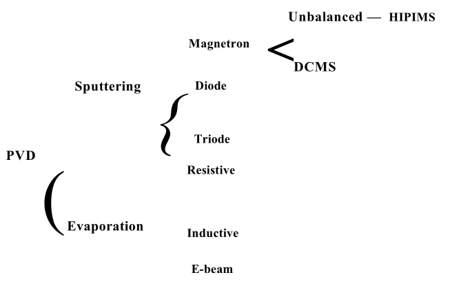
substrate at low temperature to form the film. Figure 1 shows the two major types of PVD process.
<
Unbalanced — HIPIMS{
Magnetron
DCMS
(
Sputtering Diode
Triode
PVD
Resistive
Evaporation Inductive
E-beam
Figure 1 Hierarchy of PVD system
2.1.1 Fundamentals of Plasma
Over the last two-three decades, plasmas have been extensively studied and utilized in various fields of surface engineering processes with desired functional properties. Basically “Plasma” is quasi-neutral ionised gas containing a mixture of positive, negatively charged particles and few numbers of un-ionised neutral atoms or molecules. The fundamental mechanisms which sustain and stabilize the plasma are ionisation and recombination, excitation and relaxation. The detailed explanation of these processes can be seen in [21, 22]. All these mechanisms will be initiated as a consequence of inelastic collision between electron and neutral atom. The primary electron knocks out the outer most electron from the neutral atom and produces a positive ion along with two electrons. This process For example in Ar atmosphere can be equated as,
In order to sustain the plasma, it is very essential to maintain the balance between electrons and ions, as continuous recombination process (by 3-body collision) might reduce the number of electrons.
[image:26.612.122.450.79.293.2]Hence to sustain the plasma, requires an additional external energy source which is
—)
electric field (E) in this case, can act on these charged particles and maintain the balance between electrons and ions produced by ionisation process. Effectively, the electric field can energise and accelerate the electrons produced during primary ionisation process, which results in to more ionisation due to further ionising collision process (avalanche) between these accelerated energetic electrons and neutral atoms. Besides electron impact ionisation, there are several other ionising collisions which takes place inside the plasma which sustains its glow, For example dissociative collision, ion-neutral atom collision, metastable-neutral atom collision, metastable-metastable atomic collision etc. But the ionising probability by these collision processes is very less compared to electron impact ionisation as electric field interact less with heavy ions and neutral atoms. Figure 2 shows the energy transfer mechanism from electric field to the electron
[21].
Work done
£e t 2
2 m,
Acceleration
0
ElectronAcceleration
Ion
m t
? 2
' pt e t
2
m t
LQUIIIIRIIIM DISTRIBUTION (MAX W[ ILIAN)
INELASTIC COLLISION CROSS SECTION o
EFFECT OF \ ELECTRIC F I E L D S
tA
O EFFECT OF
INELASTIC COLLISIONS
THRESHOLD
ENERGY ELECTRON ENERGY
Figure 3 The electron energy distribution function; when electric field is applied and inelastic collision cross section [Ref: 22].
The average electron energy was reported to be about 2-8 eV. Whereas the average energy of ions and neutral atoms are much less (0.03 eV at 300 K) as compared to electrons due to their limited interaction with the electric field [21]. But in practice, the plasma processes will takes place in low pressure atmospheres. At these conditions electron energies are characterised by a term kTe, where Te is the electron temperature. The electron temperature (~ 23000 K) is always yield higher value than ion temperature (~ 500 K) and neutral gas atom temperature at low pressure plasmas. Thus, highly energetic electrons participate very effectively in high temperature plasma chemistry, although the actual temperature in the gas is low [23]. Following paragraph (A) briefly summarises about electron energy distribution function in glow discharge plasma with their energy state in terms of electron temperature Te.
A. Electron energy distribution [Fe(E)]
[image:28.612.128.432.56.257.2]Hence, the presence of electric field will over populates these electrons towards higher energy regions of Maxwellian distribution. Electron energy distribution functions are measured by electrostatic probe analyzer and its energy state is always characterised in terms of electron temperature Te.
B. Sheath, plasma potential (Vp) and floating potential (Vf)
Bulk plasma can be explained as a quasi-neutral region, where charge densities nearly cancel each other. The charge density neutrality was realised to disturb the bulk plasma at the plasma-solid interfaces. Here, the solid surface refers to surfaces of cathode and substrate walls. As a consequence there will be a potential drop across the solid surface. The potential drop across this region depends upon the charge separation between the bulk plasma and solid surface [24]. A schematic diagram of this plasma- surface interface is shown in Figure 4. This interface region is called “Sheath Inside the plasma, high temperature electrons (dominant negative charge careers) masses are less (1/1823 amu) than ionic mass. Their response to the applied electric field is quite random and faster than ions [21]. This electronic response inside the plasma and across the sheath varies with respect to whether electrode surface is non-conducting (also called Floating electrode) or conducting. If the solid surface is electrically neutral, the charge imbalance would slowly develop space charge (p) across the sheath by repelling electron and attracting ions towards it continuously. This space charge can be given as [24]:
e
0
[v*iF] = p
(2>
Where, e0 = permittivity of free spacer 8.854 x 10" F/m,
V * E = variation of potential across the sheath, p = rif — ne Space charge.
The charge flow across the sheath will be controlled by the electric field caused due to space charge p. At this situation, the potential formed inside the plasma is called
conducting, the electric field changes and it allows net current to flow across the sheath due to the modified space charge distribution and electric field E [24]. The amplitude of
this case is different than those in the case of the isolated (unbiased) electrode.
Figure 3 Schematic of plasma-surface interface region showing the potential drop from cp to zero, where X is distance from grounded electrode surface [Ref: 26].
Assuming "nes" as number of electrons with average velocity ues (averaged over Maxwellian form), moving randomly across the sheath edge at potential difference of
VP — Vf ; the expression for electron current can be given as [24]:
this current is limited by the current source. The charge distribution and voltage drop in
V(x)
s
X1 — r e V 0 1
) e
= ^ e n esuesexp[ — ]
(3)
Where,
Similarly expression for ion current is given as [25],
(4)
Where,
Q
— average ion charge state1
When electrode surface is floating, both electron current and ion currents flowing across the sheath edge are equal. In this situation the floating potential Vf can be given as
Vr =
J— — ln [-^ -]
2e l2nme J(5)
v 7Based on above these equations, values of ]e, ji
and
Vf were calculated respectively for argon plasma which can be seen in [24]. When electrode surface is conducting or biased (second case), the charge separation becomes complex, so as Eq. (2). More elaborate explanation for Eq. (2) and solution for this equation finding the space charge that limits the current at biased condition have been explained by Child [26] and Langmuir [27].C. Debye Length (AD)
If the bulk plasma is not disturbed, then the net coulomb interaction with a particular charge “q” (electron or ion) sums to zero. If suppose the plasma is perturbed, then the spatial variation in the potential V(x), with respect to this charge “q” always tries to oppose this perturbation. Conversely, this perturbation can be realised within certain distance from this charge “q” [21]. This length is termed as “Debye length”. The expression for this length can be given as:
(6 )
This length describes the effective perturbation attenuation length inside the plasma [21]. The sheath thickness is always greater than the Debye length with respect to the voltage across the sheath. Hence Debye length can be used to calculate Sheath thickness when the electrode is biased, and expression can be given as [24]:
s = —3 U K k T e J
(7)
D. Plasma Frequency (f)
forces. This restoring force is in turn directly proportional to the displacement of electrons from its equilibrium position. The equation for this restoring force exerted by (E), can be given as:
m * T t = _ e <A>’ (g)
d A - n e 2 . / r .x
m^ = — A
W
Here, A is the displacement of electrons by electric field perturbation, which in turn is a function of time. The equation (9) is an equation for simple harmonic oscillator with angular frequency "a)e ", which can also be called in this case as “Plasma frequency”,
l
with the value of about 8.98 x 10³ 72e 2 Hz, where
ne
is the density per cm3. Since, theinteraction between ions and the electrons determine the plasma frequency; this can also be correlated to the Debye length. Time required for an electron to travel one Debye length is the time required for the electrons to shield the plasma from applied field (E), Hence the plasma frequency is equal to the inverse time required for an electron to travel a Debye length [21]. Approximately this frequency can be given as [26]:
o)e =
9000
(10)
So, plasma frequency "a)e " is the minimum frequency for propagation of longitudinal waves in the plasma.
2.1.2
Plasma Discharge
differ with respect to individual materials processing. The following section discuss only about DC discharge as authors Ph.D thesis work is based on this principle. More detailed explanation on RF discharge mechanism and RF generated plasma can be read in [21].
A. The DC discharge
The most simple configuration and geometry utilized from history to produce glow discharge plasma is DC discharge configuration. Figure 4 shows simple DC discharge configuration where potential difference of (V) is created between two opposing electrodes (Cathode and Anode). In general a DC power supply will be used to create this potential difference. Though glow discharge plasma appears very simple, the bulk regions and boundaries inside the chamber containing plasma are complex in nature.
High-Voltage DC Power Supply >
Anode Cathode
Figure 4 Simple DC discharge. DC power supply is connected across cathode and anode [Ref: 28].
Cathode dark space:
The region corresponding to sheath, where secondary electrons are accelerated and enter negative glow region assisting ionisation by excitation.
Negative glow:
Very bright glow region where predominant excitation-recombination mechanism takes place. In this region primary electrons were expected to consume fully their energy and it continues to extend until their travel distance from cathode.
Positive column:
Largely occupied discharge region between the cathode and anode. Most likely resembles plasma and hence predominantly used region for measurements carried out by classic probes. The electric field in this region assist in transporting the discharge current from negative glow to anode.
Aston
Dark Negative Space Glow
(AD) v (NG)
Faraday Space
(FS)
Cathode
Cathode
Glow Dark SpaceCathode
Positive Column
(PC)
Anode Anode Dark
Glow Space (AG) (AD)
Anode
These are the factors which decide the break down voltage of a gas which results in the sustained plasma discharge. The curves meeting the conditions for gas breakdown with respect to back ground pressure (for air and Ar) and inter electrode distance were obtained drawn by Paschen. Figure 6 shows the Paschen curves for gas breakdown
between two electrodes in air and Ar atmosphere. These curves can be used to decide the exact operating conditions for steady plasma discharge.
EDOO
PASCHEN r e la tio n s h ip
Q
5 2000
< P
5 1000
i—
o a .
5 500
oa < w
g 200
ARGON
100 L.
0.1 0.2 0.5 1 2 5 10 20 SO 100
[image:35.614.94.475.160.400.2]pd (Torr cml
Figure 6 Paschen curve showing the possible gas (in air & Ar) breakdown conditions
between electrodes at 20 °C [Ref: 22].
B. Secondary Electron Emission
electrons will also play a very significant role in the growth of sputtered film which will be discussed later.
2.1.3 Sputtering
Sputtering is a Non-thermal physical process where atoms are ejected from the solid surface when ions or neutral atoms with energy of few keV, are impinged on it. The kinetics of bombardment which leads to ejection of atoms from the surface is a function of series of binary collisions which can be characterised by energy transfer function given by [2 1]:
_ 4m (m t
(m i+ mt ) 2
Where, m t and m t are the masses of colliding species. From above equation, it is clear that sputtering of atoms also depends upon the mass of incident ions. Overall energy transfer is not restricted to single atomic layer, rather to several atomic layers beneath the surface through the collision cascade mechanism. During this collision cascade, momentum exchange is the dominant mechanism which sputters the atoms bound beneath the two or three atomic layers from the top surface. Sputtering can be measured by a quantity called “sputtering yield (S)”. Sputtering yield can be defined as the number of target atoms ejected per incident particle. This depends upon the type, energy and angle of incidence of the particle [22]. Figure 7 shows the experimentally determined sputtering yield for various metal targets as Ar+ ion energy under normal angle of incidence. Initially up to 20-40 eV sputtering yield low and gradually increases linearly until about 100 eV. At higher energies, the yield increases sub-linearly with ion energy. Detailed analysis of dependence of the yield on the angle of incidence can be seen in [27].
A. Sputter Deposition
Sputter deposition is the deposition of vaporised atoms ejected from a target surface, by physical sputtering process as explained in the above paragraph. The deposition processes are generally carried out in low pressure vacuum environment at working pressure of about than 5 mTorr to avoid gas phase collisions with the energetic sputtered particles. As sputter deposition technique nowadays are widely used in depositing thin films of hard coatings, coatings of architectural glass, magnetic films, semiconductor materials etc; in the coming sections of discussions reader can overview selective advanced sputter deposition techniques such as simple DC sputter deposition, Magnetically enhanced DC sputter deposition (DCMS), Cathodic arc deposition technique and High Power Impulse Magnetron Sputtering (HIPIMS) technique.
B. DC sputter deposition technique
V PLASMA
POWER SUPPLY
VACUUM CHAMBER VACUUM
[image:37.614.189.405.320.585.2]PUMPS
Figure 7 A simple parallel plate DC sputter deposition system. [Ref: 22].
voltage (V) is applied to this target. The substrates are placed at a distance of few cm away from the cathode which are electrically grounded or conducting (biased) “Anode”. The whole system will be furnished in a vacuum chamber. Ar gas is introduced inside the chamber to some predetermined pressure value. The electric field will energise and accelerate electrons which in turn engage with collision with Ar atoms and result to ignite glow discharge plasma. Brief explanation on DC discharge plasma was discussed initially in this chapter. During this process, electrons will be attracted towards anode causing more ionisation; Ar+ ions will be attracted towards cathode, finally leading to sputtering. Due to this motion of charged particle discharge current “I” flows. The voltage “V” applied to the sputtering target, which drives the current “I”, depends upon the gas pressure “P” in the vacuum chamber [21]. The deposition rate in this case relies on the amount of atoms sputtered from the target, which in turn rely on the “plasma density” near the target. This plasma density is drives the current “I” linearly on the target. But as sputtering yield also decides the amount of sputtering atoms, voltage “V” also plays a very important role in the DC sputtering system. For most of the industrial purposes, planar target DC sputtering systems are used. The film properties directly proportional to the amount of metal ions sputtered from the target (necessarily high) and the amount of metal ions can be achieved by increasing the sputtering yield. Normal attempt to increase the deposition rate is by increasing the sputtering yield, i.e by increasing the target voltage “V”. Optimum operating conditions for DC sputtering system was given in [22]. Those are listed below:
Cathode current density - 1 mA/cm2
Discharge voltage-3 kV
Ar Pressure - 75 mTorr (10 Pa)
Deposition rate - 40 nm/min
Disadvantage of DC sputtering system:
High plasma impedance was observed which lead to very low discharge current of few mA/cm2 at higher target voltage of several kV.
Non-uniform sputtering of atoms leads to poor carriage of metal atoms to the substrate surface leading to poor quality films.
2.1.4
DC Magnetron Sputter deposition technique
In mid 1970’s the invention of magnetically enhanced DC sputtering technique by Chapin was considered to be a major breakthrough in thin film technology [29]. The aim of his work was to completely come up with the solution for the disadvantages found with conventional DC magnetron sputtering.
The process of ejecting atoms or molecules from magnetically confined solid surface, in a low pressure, non-reactive/reactive ambient atmospheric conditions (of the order 0.2- 2 millitorr) can be termed as "Magnetron Sputtering". The application of magnetic field by connecting the magnets to cathode was realized after the necessity of high purity film, high deposition rate, low working pressure, ease of sputtering any metal, alloy or compound, with high adhesion to the substrate, ability to coat heat-sensitive substrates, uniform deposition, etc. These were often difficult to achieve in traditional vacuum coating techniques such as thermal evaporation and electron-beam evaporation. The principle of magnetron operation can be known by understanding the direction of magnetic and electric field confinement inside the vacuum chamber and electron drift motion, which in turn depends upon the configuration of magnetron. Basically, the magnetic and electric fields were configured on the cathode surface in
■■ > - >
The history of research and development in the PVD field has introduced variety of magnetrons configurations. For example, S-gun type magnetron, planar magnetron, cylindrical magnetron [33]. Figure 8 shows the more detailed design of planar
magnetron system.
Permanent magnets Mognetic field Lines
A 7 7A A A / A A ' T A / A A
Pole-piece J
Wafer in
J a rg e t
_ farfh shield
I, nnfr V\
W ater out 'W ater- cooled Cu
Negative
Figure 8 Schematic of Magnetron Source [Ref: 34]
^ F i e t d l i n e s - — ^ _
'Ti •« •
n
P e r m a n e n t m a g n e t s
jgLjAJL tj-j
/ ^ -nN___
FI— [FT!--- [T
P o l e - p i e c e s
»• *■ N V 1*.* *1*
Figure 9 Possible geometries of magnetrons with tunnel shaped magnetic fields
[Ref: 34].
A. Advantages of DC magnetron sputtering
The primary advantage of DC magnetron sputtering over DC sputtering can be seen in terms of (1) high deposition rate in the rage from 1 nm/s to 10 nm/s. (2) Very efficient in sputtering of metal, alloy or compounds with high purity films. (3) Good adhesion of coatings can be achieved with the substrates. (4) Ability to coat heat- sensitive substrates (5) comparatively good uniformity over the substrates with broadly tunable properties (6) High discharge currents of about 1 A to 100 A at typical voltage
of 500 V can be achieved due to low impedance observed in the plasma.
2.1.5 Cathodic Arc deposition
Arc deposition techniques were utilized since 1970’s [37, 38] and still active in industrial applications for depositing metals and refractory compounds. This technique has demonstrated its efficiency in producing high density coatings with small grain size and higher adhesion to the substrates [39].
size cathode spots [42]. Previous research articles have reported that these cathodes spots possess average current density of 10"12 Am'2. Some literature have articulated the
cathodic arc as local “explosive” event where phase transformation of spot area leading to achieve fully ionised plasma densities in the cathode region up to 1020 m' 3 [43]. The
generation of spots, its ignition and the life time on the cathode depend upon how thermal runway condition is achieved on the cathode surface [43]. Collective electron emission is a localised phenomenon, which is a result of high local electric field strength achieved on the cathode surface due to the voltage drop at sheath. This localised emission of electrons creates a spot which causes further localised ohmic heating of the emission sight. This process leads to higher electron emission with very high localized temperature reaching near the melting point of material (4000 to 7000 °C). All these events occur in a less than 10 ns [40]. The plasma emitted from the spot expands at the rate of 104m/s which contract the sheath thickness [40]. This contraction
Anode
Cathode
+ Ion Cloud
Electrons
Metal Ions
[image:43.612.182.361.29.255.2]Neutral Atoms Droplets (
Figure 10 illustrates the possible mechanism of plasma interaction during the cathodic arc deposition technique [Ref: 42].
2.1.6 Unbalanced Magnetron Sputtering
T.E.Sheridan [50] has showed long range electron and ion transport in the unbalanced magnetron plasma which was attributed to an ambipolar diffusion process can be considered as further advantage in this geometry. S. Kadlec et al. has further proved the importance of unbalanced magnetron geometry during the deposition of tin, where ion to neutral flux can be increased by a factor of 6 [51].
Figure 11 Magnetic field lines on the cathode surface; (a) balanced and (b) unbalanced magnetron case respectively. [Ref: 49].
A. Closed field Unbalanced Magnetron Sputtering (CFUBM)
geometry will be shown later as all the experiments of this work were carried out in this configuration.
2.1.7 High Power Impulse Magnetron Sputtering (HIPIMS)
In the early 1990’s, “impulse” induced ionised PVD (IPVD) technology, named HIPIMS was introduced. By definition of impulse means, atoms sputter from the target when peak power of individual pulse exceeds the time-averaged power by typically two orders of magnitude with long holds between individual pulses [55]. The technology has taken a new turn in the field of thin film coating and nanofabrication industries to deposit high quality films of metals, alloys, and ceramics, beside all these, very importantly in depositing insulating oxides and nitrides, such as A I 2 O 3 , ZnO and SnC>2. This was mainly attributed to the higher fraction of ionised sputtered material found in the HIPIMS plasma which significantly optimises the film growth and enhances the quality of deposited film.
The Initial stages of research on HIPIMS was started by Kouznetsov et al [56], where significant increase of sputtered metal ionisation during the deposition was achieved due to the utilization of pulsed power supply on Cu target. In this case, the peak target power density attained on Cu target was reported up to 2.8 kW cm' , which has resulted the peak ion current density value to reach up to 3.4 A cm' at the substrate. Similarly, in many other examples of HIPIMS research, the target power values of >1 kW cm"2 was reported [57, 58-60]. These extremely high target power densities
dissipated during HIPIMS have produced highly dense metals and gaseous ions in the
10 1
condensing flux of the plasma (order 10 m ') [57, 60-63] with more fraction of highly ionised metal ions compared to gas ions [61, 64]. Thus results obtained during HIPIMS deposition, such as dissipation of high target power density with high density metal ion plasmas condensing on to the substrates have enhanced ion bombardment on substrates. As a result the adatom mobility during the coating growth is accelerated on substrates. This has been a very essential impact of HIPIMS in producing defect free and more dense coatings when compared to conventional magnetron sputtering technique [65,
6 6]. Besides densification of coating films, HIPIMS has also shown advantages in
A. Electrical Parameter o f HIPIMS technique
The electrical parameters of the HIPIMS power supply provides necessary information on the nature of the pulses generated. During coating deposition, the applied individual pulses of HIPIMS known to deliver average energy of 2 to 8 MW, with typical
_ -200
<u -400
CD
ro
3 -600
>
"S -8000)
H -1000
O '
150
100
0 100 200
Time (us)
Figure 12. Temporal variation of cathode voltage and discharge current with respect to gas pressure [Ref: 69].
i anode
1 cathode
Trigger circuit
Charging circuit DC power
supply
Figure 13 Circuit diagram explaining HIPIMS pulse generator with a pre-ioniser circuit [Ref: 69].
Ehiasarian et al. [76] demonstrated a HMP 6/16 pulse generator capable to supply 6
MW power in 0-200 ps pulses at 0-100 Hz frequency. Besides maintaining the pulse width, HIPIMS power supplies have also designed to detect arcs and suppress it during the deposition. More arcing during the deposition process could be detrimental to the target and generate macroparticles. Christie et al. [77] and Sproul et al. [78] suggested two methods for detecting the arcs. One way is by noticing high threshold value of current and another way is by detecting the sudden decrease of voltage value. When this arc is detected the capacitor and inductor will be disconnected without any current flown through it. Further this inductor will be disconnected from the load, and thus produces few ps order delays in the discharge pulse [79]. Helmerson U. et al. [69] suggested that this delay in pulse length can be generated only if sufficient delay in discharge breakdown time is achieved. This can be accomplished by connecting low current dc pre-ioniser in the HIPIMS circuit (Figure B) [69].
B. Industrial scale up of HIPIMS
-1
Ti target in Ar atmosphere at a pressure of 1x10' mbarr. Highly ionised plasma containing doubly charged Ti2+ with extremely high metal ion-to-neutral ration was achieved for high power pulses applied at power densities of up to 3 kW/cm' generated at discharge voltage of up to 2 kV. The metal ion-to-neutral ion ratio was reported to be
, 1 ,
increased due to the rapid increase in Ti , Ti metal ion intensity at the expense of TiO emission. This was attributed to the increase in the discharge current achieved during high power impulse applied on the target. Time evolution of HIPIMS discharge measured in this industrial scale experiment has shown the transition from gas to metal plasma within the pulse [80].
C. Substrate pretreatment by HIPIMS
Performance of the coating in most of the real world applications depends upon its adhesive bonding with the substrate on which it has been deposited. Substrate pretreatment prior to the deposition of coating deposition is very essential for this purpose and is a part of plasma processing. Pretreatment for substrate surface aims to remove contaminants existing on the surface, which might act as detrimental nucleation sights during the initial stages of coating growth and defies defect free coating. Although, several chemical sputtering processes are utilized for this purpose, the traces of oxygen contaminants still observed on the surface which paves the way to grow weak microstructure. Physical sputtering technique has shown significant advantage for pretreating the surface when compared to chemical sputtering technique. This technique implants the metal ions below the substrate surface to about 5-10 nm. This changes the gradient stress at smaller scale and improves the adhesion of the coating to the substrate. The depth of implantation range rt is directly proportional to the bombarding ion energy, can expression can be given as:
n ~ Ei2m (13)
when arc technology was used for pretreatment by Ti ion. Majority of Ti atoms sputtered during arc pretreatment were found to be doubly and triply ionised with only 20% of gas is ionised [84]. HIPIMS of Nb, V, and Cr was successfully used for surface pretreatment of High speed steel substrates prior to the deposition of CrN/NbN, TiAIN, and CrAIN coatings respectively [85]. Ehiasarian et al. showed that, HIPIMS pretreated interfaces in all the above three cases were atomically very clean without any oxide contamination. Moreover the crystallinity of the interface was not deteriorated. When compared with gas ion, and Arc etched coating-substrate interfaces, HIPIMS of metal ion etching has shown superior adhesion of the coating to the substrate.
2.2 Thin film microstructural evolution
The diverse application of polycrystalline films in the field of optics, electric, magnetic, mechanics and tribology, was realised in the mid 19th century when Sir William R. Grove discovered the mechanism of sputtering to deposit thin films [8 6].
The increasing demand of real world applications in above mentioned fields have also driven equal interest in understanding the mechanism behind the microstructural growth of thin films and procedures for its effective control. Thin films exhibit different microstructures, characterised by its grain size, crystallographic texture, phase and chemical composition. These individual characteristics can be varied by various atomistic deposition processes which follow its own parameters to control the microstructure. Extensive literatures are available, which describe the basic relationship between the film microstructure and plasma processing parameters influencing this microstructure. Understanding this relationship is very crucial since microstructural properties impact directly on the functional properties of thin films which decide its quality. Universally accepted model is Structure Zone Model (SZM) proposed by Movchan and Demchishin in 1969 [87] for the growth of Ti, Ni, W, ZrC>2, and AI2O3
coating. The atomic odyssey explained in this model was based on shadowing, surface diffusion, bulk diffusion and desorption process. The sequence of these processes and as resulted microstructure of the film was modelled on the basis of melting temperature of condensates and substrate temperature. Detailed review of this model can be seen in [8 8]. Thus the importance of microstructure on the coating performance has led to
depends upon several factors such as ion-to-neutral ratio, substrate bias voltage etc. In following paragraphs, brief overview has been done on SZM for sputtered films.
A. Basic SZM for sputtered film
In early1977, J. A. Thornton [89] proposed a basic SZM for metal coatings of Ti, Cr, Fe, Cu, Mo and Al. This model was based on 20 to 250 pm thick coating deposited by magnetron sputtering. Figure 14 shows SZM explaining the evolution of morphology for above mentioned coatings based on substrate temperature and inert sputtering gas pressure (P). According to this model, at low temperature, i.e. lower Ts/Tm zone 1 structure which appear in amorphous as well as crystalline deposits were reported to be the result of shadowing effects which leads to increase in adatom surface diffusion and subsequent thickening of film density [87]. As a result zone 2 evolves which can be attributed to the surface diffusion controlled growth. Grain coarsening process i.e., recrystallization through lattice and grain boundary (GB) migration was reported to be a dominant process at high temperatures [8 8], resulting into equixed recrystallized grains
of zone 3. At the same conditions, dense array of poorly defined fibrous grains called zone T, a transition region between zone 1 and 2 occurs during
![Figure 3 The electron energy distribution function; when electric field is applied and inelastic collision cross section [Ref: 22].](https://thumb-us.123doks.com/thumbv2/123dok_us/750392.580398/28.612.128.432.56.257/figure-electron-distribution-function-electric-applied-inelastic-collision.webp)
![Figure 6 Paschen curve showing the possible gas (in air & Ar) breakdown conditions between electrodes at 20 °C [Ref: 22].](https://thumb-us.123doks.com/thumbv2/123dok_us/750392.580398/35.614.94.475.160.400/figure-paschen-curve-showing-possible-breakdown-conditions-electrodes.webp)
![Figure 7 A simple parallel plate DC sputter deposition system. [Ref: 22].](https://thumb-us.123doks.com/thumbv2/123dok_us/750392.580398/37.614.189.405.320.585/figure-simple-parallel-plate-sputter-deposition-system-ref.webp)
![Figure 10 illustrates the possible mechanism of plasma interaction during the cathodic arc deposition technique [Ref: 42].](https://thumb-us.123doks.com/thumbv2/123dok_us/750392.580398/43.612.182.361.29.255/figure-illustrates-possible-mechanism-interaction-cathodic-deposition-technique.webp)