Two-Dimensional Electron Systems
Thesis by
William Elbridge Chickering
In Partial Fulfillment of the Requirements for the Degree of
Doctor of Philosophy
California Institute of Technology Pasadena, California
2016
c
2016
Acknowledgements
This thesis and the several years of research that preceded it could not have been com-pleted without the love and support of my colleagues, friends, and family. First and foremost, I want to thank my incredibly patient wife, Theresa, who was always there for me, vicariously enduring the highs and lows of my extended academic journey.
I was fortunate to share my time at Caltech with many brilliant labmates. I am particularly indebted to Ghislain Granger who tutored me in the art of low temper-ature physics and device fabrication. Many thanks also go to Erik Henriksen and Johannes Pollanen who animated our underground laboratory with their good hu-mor and endless curiosity. And to Debaleena Nandi and Trupti Khaire for our many conversations about life and the world above ground.
Abstract
The subject of this thesis is the measurement and interpretation of thermopower in high-mobility two-dimensional electron systems (2DESs). These 2DESs are realized within state-of-the-art GaAs/AlGaAs heterostructures that are cooled to tempera-tures as low as T = 20 mK. Much of this work takes place within strong magnetic fields where the single-particle density of states quantizes into discrete Landau levels (LLs), a regime best known for the quantum Hall effect (QHE). In addition, we review a novel hot-electron technique for measuring thermopower of 2DESs that dramatically reduces the influence of phonon drag.
Early chapters concentrate on experimental materials and methods. A brief overview of GaAs/AlGaAs heterostructures and device fabrication is followed by de-tails of our cryogenic setup. Next, we provide a primer on thermopower that focuses on 2DESs at low temperatures. We then review our experimental devices, tempera-ture calibration methods, as well as measurement circuits and protocols.
Latter chapters focus on the physics and thermopower results in the QHE regime. After reviewing the basic phenomena associated with the QHE, we discuss ther-mopower in this regime. Emphasis is given to the relationship between diffusion thermopower and entropy. Experimental results demonstrate this relationship per-sists well into the fractional quantum Hall (FQH) regime.
Contents
Acknowledgements iii
Abstract iv
Introduction and Summary 1
1 Two-Dimensional Electron System 7
1.1 GaAs/AlGaAs Heterostructures . . . 9
1.2 Device Fabrication . . . 15
1.2.1 Hot-Electron Thermocouple . . . 19
1.2.2 2DES Diving Boards . . . 20
1.3 Summary . . . 22
2 Cryogenic Environment 24 2.1 Energy/Temperature Scales . . . 24
2.2 Dilution Refrigerators . . . 26
2.3 Cold Finger . . . 28
2.4 Connecting and Cooling the 2DES . . . 30
2.5 Sample Illumination . . . 32
2.6 “High” Temperature Regulation . . . 33
2.7 Summary . . . 33
3 Thermopower of 2D Electrons 35 3.1 The Seebeck Effect . . . 35
3.3 Mott’s Formula . . . 39
3.4 Thermopower vs Entropy . . . 42
3.5 Phonon Drag Thermopower . . . 44
3.6 Summary . . . 48
4 Diving Board Technique 49 4.1 Diving Board A . . . 50
4.1.1 Temperature Calibration . . . 51
4.1.2 Measurement Protocol . . . 56
4.1.3 Experimental Results at Zero Field . . . 59
4.1.4 Long Thermal Relaxation Times . . . 63
4.2 Diving Board B . . . 65
4.2.1 Short Thermal Relaxation Times . . . 67
4.2.2 Temperature Calibration . . . 68
4.2.3 Measurement Protocol . . . 70
4.3 Summary . . . 71
5 Hot-Electron Thermocouple 73 5.1 Device Layout . . . 74
5.2 Temperature Calibration . . . 77
5.3 Measurement Protocol . . . 81
5.4 Experimental Results . . . 82
5.5 Future Work: Metal-Insulator Transition . . . 88
5.6 Summary . . . 92
6 Quantum Hall Effect 94 6.1 Classical Hall Effect . . . 95
6.2 Landau Level Quantization . . . 98
6.3 Electron Spin . . . 102
6.4 Filling Factor . . . 103
6.6 Compressibility . . . 106
6.7 Edge States . . . 108
6.8 Quantum Magnetotransport . . . 110
6.9 Quantum Lifetime . . . 115
6.10 Summary . . . 116
7 Thermopower in the Quantum Hall Regime 119 7.1 Classical 2DES in a Magnetic Field . . . 120
7.2 Thermoelectric Currents . . . 123
7.3 Thermopower with LL Quantization . . . 125
7.4 Entropic Model . . . 129
7.5 Disorder and the Generalized Mott Formula . . . 132
7.6 ComputingSd xx and Sxyd . . . 133
7.7 Phonon Drag in the QH Regime . . . 136
7.8 Experimental Results at Low Fields . . . 138
7.9 Summary . . . 144
8 Fractional Quantum Hall Regime 146 8.1 Fractional Quantum Hall Effect . . . 147
8.1.1 Laughlin States . . . 148
8.1.2 Composite Fermions . . . 149
8.1.3 Wigner Crystal . . . 152
8.2 Thermopower in the FQH Regime . . . 153
8.2.1 CFs atB∗ = 0 . . . 154
8.2.2 Entropic Model . . . 158
8.2.3 Disorder . . . 160
8.3 Experimental Results at High Fields . . . 162
8.3.1 Sxx vs T at ν= 3/2 . . . 163
8.3.2 Comparison to Experiment on 2D Holes . . . 166
8.3.3 Comparison to Noninteracting Disordered Model . . . 168
8.3.5 Low-Temperature Fluctuations . . . 174
8.3.6 Comparison to Entropic Model . . . 176
8.4 Summary . . . 179
9 The First Excited Landau Level 181 9.1 FQH State at ν= 5/2 . . . 182
9.1.1 Non-Abelian Anyons . . . 184
9.1.2 Thermopower of Non-Abelian Anyons . . . 186
9.1.3 Experimental Results . . . 188
9.2 Reentrant Integer Quantum Hall Effect . . . 192
9.2.1 N ≥2 LLs . . . 192
9.2.2 N = 1 LL . . . 194
9.2.3 Experimental Results . . . 197
9.3 Summary . . . 200
A Properties of a 2DES in GaAs 202 B Sample Processing 203 B.1 Sample Cleaving . . . 203
B.2 Cleaning the Sample . . . 204
B.3 Photolithography . . . 204
B.4 Etching the Mesa . . . 206
B.5 Ohmic Contacts . . . 206
B.5.1 InSn Ohmic Contacts . . . 207
B.5.2 Ni/AuGe Ohmic Contacts . . . 208
B.6 Al Top Gates . . . 209
B.7 Thin Sample . . . 209
B.8 Mount Diving Board . . . 211
B.9 Attach Heater . . . 213
C Narrow Band Lock-In Detection 216
C.1 Example: Four-Point Resistance Measurement . . . 216
D Long Thermal Relaxation Times 218 E Electrical Resistance as a Hot-Electron Thermometer 221 E.1 Introduction . . . 221
E.2 Error in ∆R Due to Joule Heating . . . 222
E.3 Error in ∆T Due to Joule Heating . . . 223
E.4 Impact on Thermopower Measurement . . . 224
F Corbino Thermopower 225 F.1 Corbino vs Hall Bar . . . 229
G Diffusion Thermopower of a Band Insulator 232
List of Figures
1.1 Band structure of a AlGaAs-GaAs heterojunction . . . 10
1.2 Illustration of AlGaAs-GaAs-AlGaAs quantum well . . . 11
1.3 MBE grown epilayers of a quantum well heterostructure . . . 12
1.4 Conduction band of delta-doped GaAs/AlGaAs quantum well . . . 14
1.5 Simple 2DES device. . . 15
1.6 Lithographically patterned 2DES device. . . 17
1.7 2DES diving board A . . . 21
2.1 Functional diagram of dilution refrigerator . . . 27
2.2 Oxford 200 TL dilution refrigerator . . . 29
3.1 Illustration of Seebeck effect . . . 36
4.1 2DES thermopower diving board technique . . . 51
4.2 Temperature calibration using Rxx vs B . . . 53
4.3 Thermal conductance of diving board A . . . 55
4.4 Quasi-DC thermovoltage measurement . . . 57
4.5 S/T vs T at B = 0 from diving board . . . 59
4.6 S vs T atB = 0 from diving board A . . . 61
4.7 Thermal relaxation of diving board A . . . 64
4.8 Layout of diving board B . . . 66
4.9 2DES diving board B . . . 67
4.10 Thermal relaxation of diving board B . . . 68
5.1 Layout of 2D hot-electron thermocouple . . . 74
5.2 Hot-electron thermocouple device . . . 76
5.3 Temperature calibration at B = 0 using 2DES resistance . . . 78
5.4 Hot-electron thermocouple measurement circuit . . . 80
5.5 ∆S/T vs T atB = 0 . . . 83
5.6 ∆S vs ∆(1/n) at B = 0 . . . 86
5.7 Thermopower in vicinity of metal-insulator transition . . . 91
6.1 Classical magnetotransport . . . 97
6.2 Illustration of Landau levels . . . 101
6.3 Disorder broadened Landau levels . . . 105
6.4 Extended and localized states within LLs . . . 108
6.5 Classical skipping orbit . . . 109
6.6 Illustration of QH edge states . . . 110
6.7 Magnetotransport measurement setup . . . 111
6.8 Integer quantum Hall effect . . . 113
6.9 Determination of quantum lifetime . . . 117
7.1 Thermopower of classical 2DES in magnetic field . . . 123
7.2 Thermoelectric current distributions in strong field . . . 125
7.3 σxy and xy vs µ in IQH regime . . . 126
7.4 Sd vs µ in disorder-free IQH regime . . . 127
7.5 Sd vs B in disorder-free IQH regime . . . . 131
7.6 Sxxd and Sxyd vs B in IQH regime . . . 134
7.7 Sg vs B in IQH regime . . . . 137
7.8 ∆V /∆Tapp vs B in low field regime . . . 140
7.9 Comparison of theory and experiment at low fields . . . 143
8.1 Partial hierarchy of FQH states within CF theory . . . 151
8.2 Disorder-free entropic thermopower of CFs in lowest LL . . . 159
8.4 Sxx vs T atν = 1/2, 3/2, and B = 0 in 2D hole system . . . 167
8.5 Sxx and Rxx vs B in FQH regime . . . 169
8.6 Sxx vs B at various T in FQH regime . . . 172
8.7 Low-temperature thermopower fluctuations in FQH regime . . . 175
8.8 Comparison of theory and experiment in FQH regime . . . 177
9.1 Rxx vs B inN = 1 LL . . . 183
9.2 Temperature dependence of Sxx at ν = 5/2 . . . 189
9.3 Comparison of T-dependence of FQH states in N = 1 LL . . . 190
9.4 Comparison of theory and experiment at ν = 5/2 . . . 191
9.5 Anisotropy and RIQHE in higher (N ≥2) LLs . . . 193
9.6 RIQHE in N = 1 LL . . . 195
9.7 Rxy and Rxx vs T in vicinity of RIQHE . . . 196
9.8 Sxx vs B in vicinity of RIQHE . . . 197
9.9 Sxx vs T in vicinity of RIQHE . . . 198
B.1 Custom vacuum chuck . . . 212
B.2 2DES diving board A prior to installation . . . 215
C.1 Four-point resistance measurement of 2DES hall bar . . . 217
D.1 T- and B-dependence of thermal relaxation times . . . 219
F.1 Corbino thermopower measurement . . . 226
Introduction and Summary
The study of two-dimensional electron systems (2DESs) has yielded many of the most important discoveries in condensed matter physics of the past several decades. Chief among these is the integer quantum Hall effect (IQHE), a rare instance of a macroscopic manifestation of quantum mechanics in which the transverse conduc-tance becomes quantized into integer multiples of universal constants [1]. The IQHE is a single-particle phenomenon that nonetheless quickly led to the discovery of sev-eral strongly correlated many-body phases of matter. The most prominent example is the fractional quantum Hall effect (FQHE) in which collective behavior results in the conductance quantizing to particular rational numberp/q multiples of the IQHE values [2]. Adding to this list of collective phases are Wigner crystallization at high fields [3], nematic ordering in high Landau levels [4], excitonic Bose-Einstein con-densates in bilayer quantum Hall systems [5], and exotic even-denominator FQHEs believed to exhibit non-Abelian exchange statistics [6].
The exploration of the rich worlds realized within 2DESs has been dominated by measurements of electrical transport. And for good reason. Compared to optical, acoustic, and thermal experiments, measurements of conductance and resistance tend to be more easily achieved. Indeed, this is evidenced by the fact that the most famous discoveries in these systems (e.g. IQHE, FQHE) are defined in terms of electrical transport coefficients. At the same time, the information contained within these coefficients is limited. This thesis presents thermopower studies of 2DESs with the goal of augmenting our picture of these systems and the collective phases found therein.
conditions. At sufficiently low temperatures, the thermopower of a high-mobility electron system is directly proportional to the entropy per electron. Originally shown [7] to hold for noninteracting electrons, this unique relationship between a transport coefficient and a thermodynamic variable theoretically also holds in many circum-stances for an interacting 2DES in a quantizing magnetic field [8]. Providing both explanatory and predictive power, the relationship between thermopower and entropy plays a prominent role in this thesis.
The experimental studies performed for this thesis mainly focus on the lowest and first excited Landau levels, within the fractional quantum Hall (FQH) regime. This is achieved by subjecting ultra-pure GaAs/AlGaAs semiconductor heterostruc-tures to low temperaheterostruc-tures (down to T = 20 mK) and high magnetic fields (up to
B = 12 T). Within this regime, special attention is given to particular collective states. These include the composite fermion metal at filling factor ν = 3/2, the enig-matic even-denominator FQH state atν = 5/2, and insulating phases associated with reentrant integer quantum Hall effects. Odd-denominator FQH states are examined more broadly. To provide context, we also consider thermopower data at lower mag-netic fields where Landau level quantization is evident but Coulomb interactions can be ignored. Away from the quantum Hall regime, we also present a novel method for measuring the zero-field diffusion thermopower of a 2DES at high temperatures and low electron densities.
In addition to experimental methods and results, a significant portion of this thesis is dedicated to providing the reader with the context necessary for appreciating and understanding this work. Material is often presented in a pedagogical style that reflects the author’s understanding. Given the limited scope of this thesis, many subjects are treated only superficially. Nonetheless, this unique compilation of topics can hopefully serve as a helpful guide to experimentalists interested in venturing into the realm of thermoelectric phenomena in 2D systems. This thesis is organized as follows:
idiosyncrasies of the 2DES make it both incredibly useful and in many ways ideal for studying correlated many-body phenomena. We discuss the significance of ultra-clean 2DESs as well as how they are realized within GaAs/AlGaAs semiconductor
heterostructures. The building-block features of the 2DES devices fabricated for this thesis as well as the devices as a whole are described here.
Chapter 2describes the cryogenic environment in which we perform experiments on the 2DES. To motivate the discussion, we consider several temperature scales that are relevant to our research. Next, we review the working principles of dilution re-frigeration by which temperatures lower than T = 20 mK are achieved. We then survey our experimental setup, describing how our 2DES devices are electrically con-nected to, yet thermally isolated from, the outside world. Our illumination technique, which releases stubborn carriers in order to achieve the highest electron mobilities, is then discussed. Finally, we explain our method of “high” temperature regulation in which we operate a dilution refrigerator in an unconventional manner to maintain a particular set of experiments at higher than usual temperatures (e.g. 0.6.T .6 K). In Chapter 3 we explain the basic physics of thermopower in the absence of an externally applied magnetic field. We show how thermopower, also known as the Seebeck coefficient, can be understood in terms of more fundamental transport coefficients. After a brief digression into the semiclassical Drude model of electronic transport, we deriveMott’s formula, a relatively simple expression of low-temperature thermopower in terms of often measurable quantities. We then consider the relation-ship between thermopower and entropy. The chapter concludes with a discussion of the phonon drag contribution to thermopower. In the context of our research, we consider this contribution a parasitic effect to be avoided. We reveal the origin of phonon drag as well as some basic strategies for minimizing its effects.
temperature gradient. However, departing from standard practice, we do not employ external thermometry to measure this temperature gradient. Rather, we exploit temperature dependent properties of the 2DES itself for this purpose. We explain both why and how our temperature calibration is implemented in this way. This method is employed for both diving board devices introduced in this chapter. Our original device, diving board A, suffers from long thermal relaxation times. We outline our quasi-DC measurement protocol, which accommodates these delays and analyze our thermopower results in zero magnetic field. We then introduce an improved device, diving board B, which overcomes the long relaxation times via an improved design thereby facilitating much faster data acquisition.
In Chapter 5we consider an alternative approach to measuring two-dimensional thermopower by reviewing our hot-electron thermocouple. Just as a junction of dis-similar metals will produce a voltage in response to a temperature difference, so too will a junction of 2DESs with dissimilar Fermi levels. This is the working principle of our hot-electron thermocouple, which is realized by electrostatically establishing different electron densities in each half of a 2DES mesa. This thermocouple forms one “bar” of a cross patterned 2DES mesa. Current is passed along the other “bar” in order to heat the electrons at the center of the thermocouple. An advantage of this heating method is that it produces far fewer phonons compared to the exter-nal heaters employed by traditioexter-nal diving board devices. This results in a dramatic reduction in the parasitic effects of phonon drag allowing the unprecedented measure-ment of the diffusion thermopower of a high-mobility 2DES at temperatures as high as T = 2 K. In this chapter, we discuss the device layout, temperature calibration, measurement protocol, as well as experimental results of this novel technique. We conclude the chapter with a proposal to utilize this technique to study the enigmatic
two-dimensional metal-insulator transition.
integers ν, that appear in the transverse resistance with the simultaneous vanishing of the longitudinal resistance. In this chapter, we survey the essential features of quantum Hall phenomena in the absence of appreciable electron-electron interactions. We begin with the classical Hall effect, proceed to Landau level (LL) quantization, explain filling factors, the impact of disorder, the notion of compressibility, and the role of edge states. Once equipped with these concepts, we are able to understand typical quantum magnetotransport measurements. We conclude this chapter with a discussion and measurement of the quantum lifetime, a quantity we reference in subsequent chapters.
Chapter 7 reviews thermopower in the quantum Hall regime. To establish con-text, we begin with a discussion of a classical 2DES in a magnetic field. We then consider how disorder-broadened LLs dramatically alter the thermoelectric response of the 2DES. In part to demonstrate that the relationship between thermopower and entropy persists in the presence of a strong magnetic field, we demonstrate that the diffusion thermopower of a disorder-free 2DES in the IQH regime can be derived by merely counting single-electron states. This chapter touches upon many subjects including how a disorder potential gives rise to a transverse thermopower, known as the Nernst-Ettingshausen effect, the current distributions during a thermopower measurement, a model for computing the thermopower tensor, and phonon drag in the quantum Hall regime. We conclude with an analysis of the results of our low-field thermopower measurements.
of CFs. The CF effective mass is extracted and compared to theory and previous measurements. The wealth of FQH state signatures in thermopower versus magnetic field measurements is demonstrated and compared to those in more familiar resistance data. More generally, the temperature and field dependence of thermopower in the FQH regime is shown to be at least qualitatively consistent with the entropy per CF for two species of CFs (2-flux and 4-flux quanta attached).
Chapter 1
Two-Dimensional Electron System
A two-dimensional electron systemor 2DES is a gas of electrons that is free to move in-plane but constrained from moving out-of-plane1. Such a system is of great utility
to those of us interested in many-body correlated physics for several reasons. First, as discussed below, it is quite practicable to separate the donor ions from the electrons that comprise a 2DES. This liberates the electrons from interacting strongly with a background potential as is the case for electrons in a metal, such as copper, or a typical doped semiconductor. In addition, being confined to two dimensions, the electrons are limited in their ability to screen the charge of neighboring electrons. Finally, when subjected to a strong out-of-plane magnetic field, the kinetic energy of low-temperature 2D electrons quantizes into discrete levels yielding thequantum Hall effect(see Chapter 6). All of these circumstances enhance the role of electron-electron interactions.
Historically there are many ways to realize a 2DES. Early studies exploited weakly polarizable surfaces such as that of solid hydrogen or liquid helium [10]. More recently, graphene—atomic sheets of carbon that form a honeycomb lattice—have attracted a great deal attention due to its many exceptional properties, including its electronic characteristics, which are governed by two-dimensional electron (and/or hole) systems [11]. Another approach involves trapping electrons in a potential energy well formed at a material interface. Using this latter technique, we are today surrounded by 2DESs formed within transistors such as the ubiquitous metal-oxide-semiconductor
field-effect transistor or MOSFET that forms a technological cornerstone of modern electronics.
In enhancement mode MOSFETs a voltage between the ’metal’ and the semi-conductor results in the formation of a 2DES at the oxide-semisemi-conductor interface. Known as an inversion layer, this 2DES allows conduction between the transistor’s source and drain. In 1980 Klaus von Klitzing made one of the most dramatic discov-eries [1] in the field of condensed matter physics by studying such inversion layers at low temperatures and within large magnetic fields. He found that at certain values of the magnetic field the transverse, or Hall, conductance became precisely equal to integer multiples of a universal value. This macroscopic manifestation of quantum mechanics, now known as theinteger quantum Hall effect(IQHE), plays an important role in this thesis and is discussed in detail in Chapter 6.
The quality of the 2DES formed within MOSFETs is limited, however, due to its relatively high scattering rate. A simple way to formalize the quality of a 2DES is through a quantity known aselectron mobilityµe defined as the ratio of the electronic
drift velocity vd to the electric field; that is, vd =µeE. Unlike the crystalline silicon
that forms the conduction channel of a MOSFET, the silicon dioxide that electri-cally isolates the 2DES from the ’metal’ electrode is glassy resulting in an interface roughness that scatters the electrons thereby limiting their mobility. As a result, a ’high-mobility’ silicon MOSFET at low temperature has µe . 40,000 cm2/Vs [9].
While this is indeed a high-mobility when compared, for example, to electrons in a copper wire at room temperature (µe ∼30 cm2/Vs), we require mobilities more than
two orders larger in magnitude to realize the delicate many-body phases of interest in our studies.
This chapter provides an overview of the devices within which the ultra-high-mobility 2DESs are realized and studied for this thesis. We begin with a discussion of GaAs/AlGaAs heterostructures and the band engineering made possible via the parameters of these layered crystalline semiconductors. We then introduce the specific devices studied along with a basic2 description of the techniques employed in their
fabrication. Subsequent chapters elaborate on these devices and how they are used to measure the thermoelectric properties of the 2DES.
1.1
GaAs/AlGaAs Heterostructures
The problem of interface roughness is largely overcome within the ultra-clean, lay-ered semiconductors known asheterostructures[12]. Using molecular beam epitaxyor MBE, extremely pure material may be grown on a substrate with nearly atomic res-olution. The most common heterostructures are made from group III-V compounds; in particular, GaAs and AlAs. These two compounds are very well matched due to having the same zinc-blende crystal structure and lattice constants that differ by less than 0.15% allowing them to be grown on top of one another without introducing appreciable stress or defects. At the same time, the band gaps Eg of these two
com-pounds are quite different: at low temperatures3, GaAs has a direct gapE
g = 1.52 eV
while AlAs has an indirect gap Eg = 2.25 eV. The goal of heterostructure growth
using these compounds is to manipulate the electrical and/or optical properties of the material by layering alloys of the form AlxGa1−xAs, wherexis a number between
0 and 1 indicating the Al concentration. This process is known as band engineering. As an example, let us consider the band structure at a heterojunctionbetween the alloy Al0.3Ga0.7As, which has a direct energy gap Eg = 1.93 eV at low temperatures,
and pure GaAs. A simple model [13] known asAnderson’s rulestates that the vacuum levels of two materials are aligned at a heterojunction. The band structure is then determined by the difference between the bottom of the conduction band and the vacuum level, known as a material’selectron affinityχ. The difference in the electron affinities then governs the discontinuity in the conduction band ∆Ec as illustrated
in Fig. 1.1. In reality, Anderson’s rule is overly simplistic and in the case of a heterojunction formed by Al0.3Ga0.7As and GaAs it overestimates ∆Ec. The actual
discontinuity has been measured as ∆Ec= 250 meV [14].
Appendix B.
3These values are forT
.4 K. At room temperature, GaAs has a direct gapEg= 1.42 eV and
Al
0.3Ga
0.7As
GaAs
vacuum level
conduc3on band
valence band
χ
E
g1.93 eV 1.52 eV
Figure 1.1: Band structure of a AlGaAs-GaAs heterojunction.
By sandwiching a layer of GaAs between layers of AlGaAs a quantum wellis cre-ated that can confine electrons of the conduction band4 in the growth orz-direction.
In Fig. 1.2 we illustrate a quantum well resulting from 20 nm of GaAs sandwiched between layers of Al0.3Ga0.7As. The dashed line in the figure represents a Fermi level
that lies below the confinement potential, or in the band gap, of the flanking AlGaAs resulting in a spatially localized electron system. Importantly, such a finite quantum well supports multiple localized modes or subbands (not shown). By positioning the Fermi level appropriately, only the lowest subband is populated. Of course, these structures are in fact three dimensional and Fig. 1.2 only shows the variation of the potential in the z-direction. Well away from the edges of the sample, electrons are unbound and free to move in the x-y plane thus establishing a 2DES.
But how is the Fermi level determined? Up to now we have neglected a critical aspect of heterostructure band engineering. Intrinsic semiconductors like GaAs, AlAs, and their alloys have Fermi levels that lie in band gaps. To create a metallic or
compressible system we must therefore introduce additional carriers. An obvious way to achieve this would be to dope a quantum well with donors. The problem with this approach, however, is that the donors, ionized after contributing their electrons, would
4In Fig. 1.1 we see the valence band of the GaAs lies about 0.04 eV above that of the Al
0.3Ga0.7As
20 nm
Al
0.3Ga
0.7As
GaAs
Al
0.3Ga
0.7As
conduc2on band
Fermi level
0.25 eV
E
z
Figure 1.2: Illustration of a quantum well created by sandwiching 20 nm of GaAs between layers of AlGaAs.
scatter the 2DES via Coulomb interactions thereby limiting their mobility µe and
preventing the formation of the delicate many-body phases we desire. The solution is to utilize the important invention by St¨ormer et al. [15] ofmodulation dopingin which dopants are spatially separated from the quantum well, far enough that scattering from donor ions is minimized but close enough that donated carriers migrate to the well. Exotic many-body phases aside, modulation doping is also extremely important to the realm of modern device physics. It has allowed the realization of high gain FETs with ultra-high switching speeds that are a crucial ingredient in the front-end amplification stages of the now ubiquitous cellular phone.
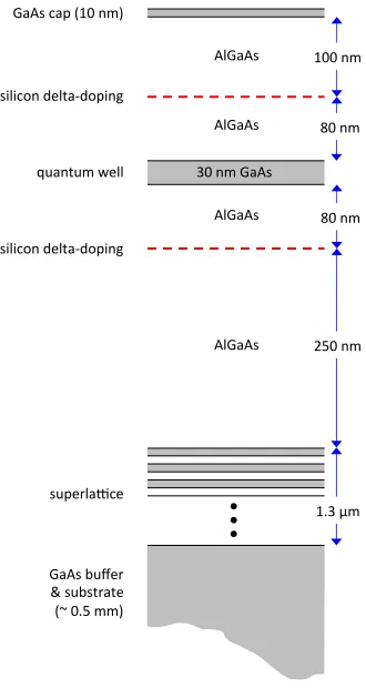
250 nm
80 nm
80 nm
100 nm
1.3 μm
30 nm GaAs
quantum well
silicon delta-‐doping
silicon delta-‐doping
superla>ce
GaAs cap (10 nm)
AlGaAs
AlGaAs
AlGaAs
AlGaAs
[image:25.612.164.494.88.717.2]GaAs buffer
& substrate
(~ 0.5 mm)
fluctuations in the background potential, and therefore, can result in higher electron mobilities. However, placing the donors too close to the quantum well defeats the whole purpose of modulation doping, which is to separate the 2DES from the donor ions. This implies there is an optimal setback distance—given the quantum well width, aluminum concentration in the AlGaAs, and other parameters beyond the scope of this thesis—that will maximize the electron mobility.
Continuing our tour of Fig. 1.3, the MBE growth begins by depositing a buffer layer of 500 nm of GaAs onto a 0.5 mm thick (100)-oriented GaAs substrate. This is followed by the growth of a filtering superlattice; that is, an array of one hundred narrow, 3 nm wide GaAs quantum wells each separated by 10 nm of AlGaAs. The superlattice traps impurities that percolate up from the substrate during growth and also prepares an atomically flat surface onto which the critical layers of the heterostructure may be grown. Growth then proceeds with 250 nm of AlGaAs5
followed by the lower donor layer and then the AlGaAs-GaAs-AlGaAs quantum well structure. Moving upward, after the upper donor layer, an additional 100 nm of AlGaAs is deposited followed by a 10 nm GaAs cap to protect the aluminum from oxidation.
Now that we have a better picture of the full structure involved in realizing an ultra-high-mobility 2DES, we may refine our diagram of the band structure. Hereto-fore we have neglected the effect of the donor ion charge as well as that of the 2DES itself on the conduction band. The bands shown in Fig. 1.1 and 1.2 reflect only the kinetic energy of the electrons in each material layer. The actual bands include an additional contribution from the electrostatic potential that arises from separat-ing electrons from their donor ions. As a rule, bands bend within charged regions with a curvature proportional to the charge density. In Fig. 1.4 we illustrate the conduction band along the z-direction for a delta-doped quantum well that includes this electrostatic potential contribution. The dashed line in the figure represents a Fermi level that is positioned above the bottom of the band within the well, thereby 5The parent wafer of the diving board devices studied in this thesis contain the alloy
populating its lowest subband whose wave function is also depicted in the figure. At the same time, the Fermi level remains below the local band minima at the donor layers precluding the formation of parallel electron systems6.
donor ion charge
2DES wave func4on
+
+
conduc4on band
Fermi level
Figure 1.4: Illustration of the conduction band of a delta-doped GaAs/AlGaAs quan-tum well that includes the contribution from the electrostatic potential resulting from separating electrons from their donor ions. The dashed line represents a Fermi level resulting in the population the lowest subband of the quantum well.
Determining the actual position of the Fermi level relative to the quantum well is not only a function of the heterostructure layers but is also governed by the situation at the GaAs cap’s exposed surface. Exposed GaAs has a high density of surface states near the middle of its band gap [9]. These states are in fact so numerous that they pin the Fermi level to their narrow band of energies lying about 0.8 eV below the bottom of the conduction band. In many cases the ability to adjust the Fermi level, and hence the 2DES’s density, is desirable. Metal may be deposited onto the surface of many7 heterostructures in order to capacitively modulate or gate the 2DES’s density by adjusting the Fermi level. Gating in this manner plays a critical role in the thermopower measurements made via our hot-electron thermocouple. We will further discuss the fabrication and behavior of gates in Section 1.2.
The combined effect of the atomically sharp interfaces and remotely located donor ions of GaAs/AlGaAs heterostructures are 2DESs with electron mobilities that can 6A common failure-mode for heterostructure growth is the manifestation of parallel conduction
resulting from a Fermi level that sits above the local minima of the conduction band at the donor layers. Fortunately, this issue is readily identified through basic magnetotransport (see Chapter 6).
7Not all heterostructures are “gatable” in this manner. See Section 1.2 for a discussion of the
exceed 3×107 cm2/Vs. This is the highest of any electron system and nearly three
orders of magnitude greater than that of the “high-mobility” silicon MOSFETs dis-cussed in the previous section. Moreover, an ultra-high-mobility 2DES with a density of 3×1011 cm−2 will have a mean free path8 of ∼ 300 µm! These state of the art heterostructures are therefore a critical ingredient to a study such as ours. We are therefore quite fortunate in our collaboration with Loren Pfeiffer and Ken West of Princeton University who consistently produce wafers of the highest quality, without which our research would not be possible.
1.2
Device Fabrication
[image:28.612.230.411.429.606.2]Once a GaAs/AlGaAs heterostructure is grown, specialized 2DES devices may be con-structed through subsequent fabrication or sample processing. This section presents a qualitative overview of commonly fabricated features. A detailed account of the actual processing recipes used to create these features is provided in Appendix B.
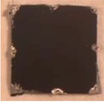
Figure 1.5: Image of a simple 2DES device. This cleaved sample is about 5×5 mm2
with eight indium ohmic contacts placed along its periphery. Simple devices like this are routinely used to characterize their parent wafers.
The most simple devices merely involve making electrical contact to the 2DES. Figure 1.5 shows a 5×5 mm2 sample cleaved from a parent wafer withohmic contact
material—in this case, pure indium—placed at the corners and midpoints of its pe-riphery. The term “ohmic contact” originates from their approximate adherence to Ohm’s law, as opposed, to say, a non-linear diode-like behavior. To fabricate these contacts the indium is carefully applied to the sample’s surface using a soldering pen. It is then diffused into the heterostructure by annealing the sample in a forming gas atmosphere. Wires are then attached through the dextrous use of tweezers, soldering pen, and a microscope. Simple devices like this are routinely used to characterize the quality of their parent wafers through measurements of the 2DES’s electrical re-sistivity (Appendix C) as well as magnetotransport (Sec. 6.8) in order to determine electron mobility.
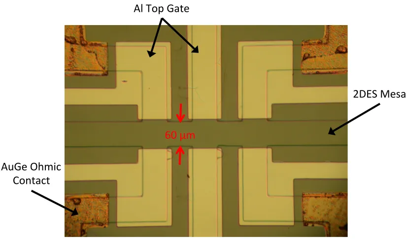
Using lithographic techniques the surface of a sample may be patterned in ways to create more sophisticated devices. For example, the 2DES may be confined to an arbitrary geometry in the x-y plane by wet etching a lithographically patterned sample9. The 2DES is destroyed within the etched region. The remaining, unetched region is referred to as a2DES mesain analogy to the table-top shaped hills common to the American Southwest. Figure 1.6 shows a sample with several patterned features including a 2DES mesa consisting of 60 µm channels.
The ability to modulate the density of the 2DES or to even fully deplete the quan-tum well is often desirable. Patterned metal, typically aluminum, may be thermally evaporated onto a sample’s surface allowing electrostatic manipulation of the Fermi level. In this way, a metallic top gate forms a capacitor with the 2DES allowing the reduction or even enhancement of the number of electrons within the quantum well (this manner of gating is critical to the operation of our hot-electron thermocouple). 9While it is common practice during mesa processing to etch sufficiently deep that the quantum
2DES Mesa Al Top Gate
AuGe Ohmic Contact
[image:30.612.115.528.85.328.2]60 μm
Figure 1.6: A lithographically patterned 2DES device. The image is filtered to en-hance color contrast.
As an example, refer to Fig. 1.6; the six mesa arms extending vertically from the central 60 µm channel are covered by aluminum top gates. Another, very simple technique is to place copper tape beneath the 0.5 mm substrate, positioned between a sample and its plastic header, to form a back gate. There are limits to this gating technique, however. In enhancement mode, a sufficiently large positive voltage (e.g.
∼ 0.5 V) can produce quantum mechanical tunneling between the 2DES and top gate. At the same time, GaAs has a dielectric breakdown field of 3−9×10⁵ V/cm
[16] setting an upper limit on the magnitude of voltage that can be applied to an external gate without damaging the sample. Copper back gates, meanwhile, have rel-atively small capacitances due to the thick substrate10. Dielectric breakdown within
the wiring will therefore determine the maximum voltage (e.g. ∼ ±200 V) for these 10Back gates can be evaporated onto thinned samples to achieve relatively high capacitances
gates, thereby limiting density adjustments to ∆n ∼ ±1010cm−2; often less than 10%
of the ungated density.
Many, though not all, GaAs/AlGaAs heterostructures are “gatable”. Samples of the highest mobility—such as those used to fabricate the diving board devices studied for this thesis—are not amenable to electrostatic gating due to mobile carriers in their donor layers that screen an electric field originating from an external metal gate. In order to achieve the highest electron mobilities these heterostructures are said to be “over-doped” resulting in potential wells at the donor layers that actually dip below the Fermi level resulting in a small degree of parallel conduction. While this parallel conductance is negligible relative to that of the 2DES it is advantageous in its smoothing of the remote impurity potential seen by the 2DES. Achieving the highest electron mobilities therefore comes at the cost of electrostatic gatability.
Another key feature of the sample presented in Fig. 1.6 are its ohmic contacts seen in the corners of the image. An alternative to the indium used for the simple device shown in Fig. 1.5, ohmic contacts may also be constructed from an evaporated AuGe alloy. To assist with adhesion, a thin, “sticky” layer of nickel is first evaporated onto the GaAs surface. Like indium, AuGe diffuses into the GaAs/AlGaAs heterostructure during an annealing treatment to make contact with the quantum well. Compared with indium, evaporated AuGe contacts usually provide a less resistive connection to the 2DES and have the added benefit of being lithographically defined. As such, they can be formed into arbitrary geometries; an important feature for the hot-electron thermocouple discussed in the next section. The only downside of evaporated contacts is the overhead involved with the requisite lithographic methods.
of the photoresist, depending on its polarity. The remaining photoresist acts as a protective layer and the exposed areas may be etched or metalized.
This patterning technique is capable of feature sizes down to about 5µm, a number set by the diffraction limit of the ultraviolet light used. One can go beyond this limit, achieving nano-scale feature sizes through the use of electron beam lithography. Modern scanning electron microscopes are readily capable of achieving dimensions as small as 50 nm, a limit set by the de Broglie wavelength of the energetic electrons used. The experiments performed for this thesis, however, focus on the diffusion transport of ultra-high-mobility electrons. As already mentioned, these systems can have mean free paths of hundreds of microns. This sets a lower bound for the feature sizes permitted in our devices if we want to avoid ballistic behavior. For this type of experiment, therefore, bigger is better and photolithography is the appropriate fabrication technique.
1.2.1
Hot-Electron Thermocouple
The hot-electron thermocouple utilizes all of the features described in the previous section. In fact, the image of Fig. 1.6 is the interior region of the sample used to acquire all of the hot-electron data presented in this thesis. A lower magnification image of the device is provided in Chapter 5 along with an explanation of the protocol used to measure thermopower.
The device originates from a 5×5 mm2 sample cleaved from a GaAs/Ga
0.3Al0.7As
heterostructure that includes a symmetrically doped 20 nm quantum well grown via MBE onto a (100)-oriented GaAs substrate. The sample has an ungated density of
n = 1.6×1011 cm−2 and an electron mobility of µe = 3.3×106 cm2/Vs, at low
realized in this device, which is designed with noninteracting electrons in mind. The device was patterned into a 1 mm-long, 60 µm-wide 2DES mesa with ohmic contacts at each end for driving current along it. Three arms extend away from each side of this central channel and terminate at ohmic contacts. The actualthermocouple
consists of the two opposing arms in the center of the device which are overlaid with top gates. The remaining arms, which are also equipped with top gates, are normally used as voltage probes enabling measurements of the resistance of the 2DES in the central region of the device.
The ohmic contacts are the evaporated Ni-AuGe variety and in addition to en-abling electrical measurements they also serve to thermally anchor the electron gas in their immediate vicinity to the lattice temperature. Away from the contacts, how-ever, the electrons can easily be heated out of equilibrium with the lattice; hence the term “hot-electron”. This fact is critical to the operation of the device and will be elaborated upon in Chapter 5.
1.2.2
2DES Diving Boards
In Chapter 4 we explain our diving board technique for measuring the thermopower of the 2DES. The 2DES diving board devices employed by this technique are both cleaved from a GaAs/Al0.24Ga0.76As heterostructure grown via MBE onto a
(100)-oriented GaAs substrate. The crucial epilayers of their parent wafer correspond to those shown in Fig. 1.3. After illumination11by a red LED, the density and mobility
of the 2DES are n = 2.9×1011 cm−2 and µe = 3.1×107 cm2/Vs, respectively, at
low temperatures. The ultra-high-mobility 2DESs originating from this wafer exhibit a wealth of fractional quantum Hall (FQH) states and other many-body correlated phenomena.
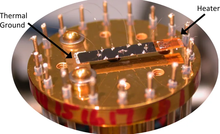
The original diving board, which we designate with the letter ‘A’, is shown in Fig. 1.7. The sample is bar shaped, L= 12 mm long by W = 3 mm wide. A strain gauge12 acting as a heater is attached to one end of the sample while the other end
11See Section 2.5 for a discussion of sample illumination.
Thermal
Ground
[image:34.612.127.501.93.321.2]Heater
Figure 1.7: 2DES diving board A installed into a special sample stage. The gold-plated silver disc is about one inch in diameter.
is indium-soldered to a small Au-plated copper slab that serves as thermal ground. The copper slab is, in turn, bolted to the cold finger of a dilution refrigerator13.
This configuration allows a heat flux to flow along the length of the diving board establishing a temperature gradient along the 2DES.
The sample’s surface is patterned into two square 3×3 mm2 2DES mesas, sepa-rated by 1 mm and positioned symmetrically about the midpoint of the bar. Electrical contact to the 2DESs is enabled by six small eutectic InSn14 ohmic contacts diffused onto the mesa perimeters. Close inspection of Fig. 1.7 reveals that the two mesas share one ohmic contact and are thereby connected in series. Manganin wires, 25µm in diameter and approximately 1 cm long, are attached to these contacts (and to the resistive heater). Manganin was chosen because the thermal conductance and ther-mopower [17] of these wires is negligible in comparison to the thermal conductance
13See Sec. 2.2 for a discussion of dilution refrigeration.
14We find that ohmic contacts made from eutectic InSn yield marginally lower resistances when
of the sample bar and the thermopower of the 2DES within it.
For reasons that will be made clear in subsequent chapters, we want to maximize the thermal resistance of the diving board. This is achieved by thinning the substrate to about t = 130 µm via a chemical etch15 and then sandblasting its backside to ensure diffuse phonon scattering [18]. This latter step is important, for otherwise highly specular phonon boundary scattering can lead to nonuniform temperature gradients along the bar.
It turns out that diving board A suffers from a problem that limits its ability to measure thermopower at low temperatures and high magnetic fields. Using fabrication methods covered in this chapter and Appendix B, an improved diving board device is constructed that overcomes these issues. We defer the discussion of both the problem presented by diving board A along with the improved diving board to Chapter 4.
1.3
Summary
In this chapter we introduced the two-dimensional electron system (2DES). Interest-ing in and of itself and yieldInterest-ing highly impactful applications (e.g. in enhancement-mode MOSFETs), the 2DES provides an ideal forum for studying strongly corre-lated quantum systems. The cleanest, highest mobility 2DESs are realized within GaAs/AlGaAs heterostructures grown via molecular beam epitaxy. These layered materials are grown such that when cooled, potential energy wells trap electrons away from their donor ions and are confined to two dimensions. By separating the negatively charged electrons from their positively charged donor ions, their interlayer interaction can be made negligible in comparison to the intralayer coupling of neigh-boring elections within the 2DES. By minimizing this background charge potential within an all but defect-free crystal lattice, inelastic scattering rates are dramatically reduced resulting in ultra-high electron mobilities.
Many years of research have resulted in a number of fabrication techniques used to create specialized devices from the wafers of these state of the art GaAs/AlGaAs
Chapter 2
Cryogenic Environment
The art of achieving, maintaining, and modulating extremely low temperatures, known as cryogenics, advanced by leaps and bounds during the 20th century. This greatly facilitated experimental condensed matter research in numerous areas includ-ing magnetism, lattice dynamics, electronic properties of materials, superconductiv-ity, and superfluidity. Likewise, in order to realize the delicate correlated electron phases that are the focus of this thesis, it is necessary to perform our experiments at sub-Kelvin temperatures.
In this chapter we first consider the energy, or temperature, scales relevant to our research. This motivates the discussion that follows on dilution refrigeration which is the means by which we cool our experiments. After a brief description of how the sample is positioned within the core of a powerful magnet, we examine both the electrical and thermal connections to the 2DES. We conclude with some words on the technique of sample illumination whereby additional carriers are coaxed into the quantum well in an effort to maximize the electron mobility.
2.1
Energy/Temperature Scales
To better appreciate our need for cryogenic temperatures, it is helpful to consider several relevant energy scales. For starters, before any quantum mechanical behavior can be resolved, our electrons must be cooled well below their Fermi temperature
2.9×1011 cm−2,T
F = 120 K. At temperatures much less than this the 2DES is said
to be adegenerate electron gas, as the lowest energy states are completely filled, and its fermionic nature emerges.
A comparable energy scale is found within the heterostructure band structure we discussed in Section 1.1. The GaAs quantum well contains several modes or subbands. To ensure that our electron system is indeed confined to two dimensions, it is incumbent on us to only populate the lowest energy subband1. For a heterostructure
like that shown in Fig. 1.3 the energy difference between the lowest and first excited subband is E1 −E0 ∼100 K. We must therefore operate at temperatures much less
than 100 K if we are to guarantee a negligible thermal population of carriers in the quantum well’s first excited mode.
In Chapter 6 we will discuss the physics of two-dimensional electrons in a magnetic field. Ignoring electron-electron interactions for a moment, at sufficiently high fields the electrons will follow quantized cyclotron orbits in a manner somewhat similar to the quantized orbits of an atom. In order to resolve this phenomenon we must cool the electrons to a temperature well below the energy difference of these orbits. The actual energy differences in question are functions2 of electron density and magnetic field
strength but a representative value for the regime studied for this thesis corresponds toT ∼10 K.
The most delicate many-body electron states require we go colder still. A key mo-tivation for our work is the interest surrounding the even-denominator fractionalized quantum Hall state at Landau level filling factorν= 5/2, which is believed to exhibit exotic quantum statistics. In our samples, as we will see, this state is associated with an energy gap of ∆≈450 mK. Fortunately, we have tools for achieving such extreme cold, most important of which is dilution refrigeration.
1In Chapter 6 we explain how to experimentally demonstrate the two-dimensional nature of the
electrons.
2.2
Dilution Refrigerators
The standard approach to reaching temperatures below about 300 mK is through
dilution refrigeration[19]. A relatively recent invention of the 1960s [20], this method of refrigeration relies upon some fortunate properties of 3He−4He mixtures. Below
about T = 0.87 K, a mixture of liquid 3He and 4He will separate into a 3He-rich phase and a 3He-poor phase. As absolute zero temperature is approached, the 3 He-rich phase will become pure 3He. Importantly, however, the 3He-poor phase will always contain a small fraction of 3He, approaching the universal value of 6.6% as
T →0. This surprising fact is critical to the operation of a dilution refrigerator (DR). Cooling occurs via the transfer of3He atoms from the3He-rich phase to the dilute,
3He-poor phase, due to the higher enthalpy of the atoms in the latter phase. This can
be qualitatively understood in analogy to evaporation in which a pure liquid cools as some of its molecules transition to a gaseous phase. By creating a situation in which
3
He atoms are continuously moved from the 3He-rich to poor phase, a state of the art DR can cool the mixture to temperatures below 10 mK!
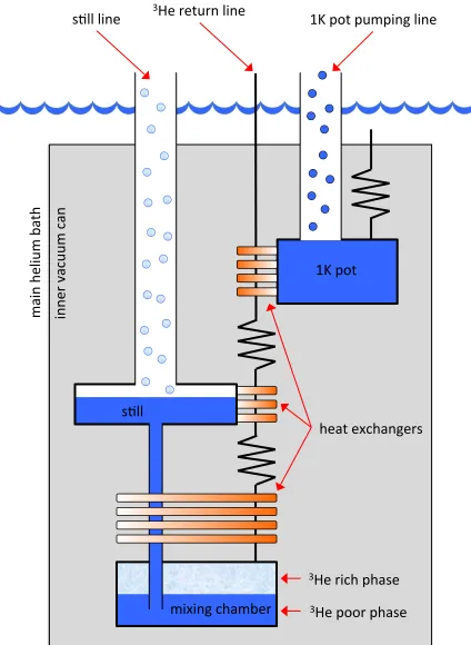
Figure 2.1 contains a functional diagram of a generic DR. To thermally isolate the DR it is enclosed within an inner vacuum can or IVC. On the other side of the IVC wall the main helium bath shields the DR from the hot electromagnetic radiation of the outside world. Inside the DR, the amount of helium along with the precise 3He to 4He ratio must be such that the phase boundary occurs in the mixing chamber. Due to the 3He-rich phase’s smaller mass density, it floats on top of the
3
1K pot
s(ll
mixing chamber
heat exchangers
m
ai
n
he
liu
m
b
ath
3
He rich phase
3
He poor phase
in
ne
r v
ac
uu
m
c
an
[image:40.612.112.536.96.676.2]
s(ll line
3He return line
1K pot pumping line
To achieve continuous cooling, the 3He removed from the still must find its way back to the3He-rich phase within the mixing chamber. Toward this end, the exhaust of the still pump is routed back into the cryostat via a high-impedance capillary called the return line. A set of heat exchangers thermalize the 3He with a volume known as the 1K pot. The 1K pot is a small reservoir of 4He—independent of the closed dilution circuit—that is continuously fed from the main helium bath. Pumping on the vapor of this 4He cools it to T ≈ 1.2 K, a temperature at which the 3He in the low-pressure (e.g. 10 mBar) return line readily re-condenses.
Following liquification, the 3He encounters the primary impedance of the return line before further cooling via another set of heat exchangers coupled to the still. Now at T ≈0.7 K, a second impedance is overcome prior to arriving at the final set of heat exchangers where thermalization with the 3He-poor phase between the still and mixing chamber occurs. Finally returning to the mixing chamber, we have come full-circle, completing the dilution refrigeration circuit.
The cooling power of a DR is harnessed by thermally anchoring an experiment to its mixing chamber (not shown in the figure). In our research we employed two different DR models. Our coldest experiments, involving the diving board devices, took place within an Oxford 200 TL shown in Fig. 2.2, which has a cooling power of about 200 µW at T = 100 mK and a base temperature of T ≈17 mK. Meanhwhile, the hot-electron thermocouple experiments were conducted within an enhanced Ox-ford KelvinOx 25 (50 µW at T = 100 mK with a base temperature of T ≈30 mK), however, we did not use this DR in a conventional manner as explained below in Section 2.6.
2.3
Cold Finger
in-1K pot
heat exchanger
thermometer
sample stage
s2ll
mixing chamber
cold finger
duced in the metal parts of the DR while changing the field strength, the magnet is located well below the mixing chamber. The sample stage is precisely positioned in the center of the magnet core via a long, highly thermally conducting set of rods collectively known as the cold finger (see Fig. 2.2). Interestingly, cold fingers are typically made using annealed silver rather than copper because the latter contains nuclear magnetic moments resulting in a strongly field dependent specific heat3. As the thermal link between the DR and the sample, an ideal cold finger would lack a temperature gradient and respond instantly to changes in mixing chamber tempera-ture.
2.4
Connecting and Cooling the 2DES
The substrates of the diving board samples are anchored to the DR’s mixing chamber via a special gold-plated silversample stagethat is shown in Figs. 1.7 and 2.2. Indium soldering one end of the sample to a gold-plated bar that is bolted to a solid silver part that is in turn attached to the cold finger provides thermal ground to these devices. While this effectively cools the sample’s GaAs substrate, achieving the lowest temperatures for the 2DES itself is another matter.
Cooling electrons below T ∼ 100 mK is a key challenge of low-temperature con-densed matter physics. High-mobility 2DESs such as ours are limited in their ability to cool via phonon emission in this so-calledBloch-Gr¨uneisen regime, with measured energy relaxation rates varying as strongly as ∝ T5 [22, 23]. To mitigate this issue,
we connect low-pass filters in series with the 2DES ohmic contacts. In the case of our diving board experiments, these filters are formed by a 5 kΩ metal-film resistor and a 500 pF capacitor, which eliminates high frequency noise that would otherwise heat the 2DES. Perhaps even more importantly, we ground the capacitors to the cold finger. The idea is that while the capacitor acts like an open circuit with respect to our quasi-DC electrical measurements, it is thermally a short circuit, connecting the 3Some cryostats exploit this property of copper, or other materials with large nuclear moments like
the intermetallic compound PrNi5, to construct cooling stages that utilize the principle of adiabatic
2DES to a reservoir of cold electrons.
A challenge complimentary to that of cooling electrons is determining their pre-cise temperature. While a calibrated carbon resistance thermometer attached to the mixing chamber (see Fig. 2.2) reliably reports the temperature of a sample’s lattice, the actual temperature of the 2DES is more elusive. Direct methods of measuring electronic temperature, such as Coulomb blockade [24], do exist but are difficult to im-plement. As will be discussed in this thesis, under certain circumstances, the 2DES’s diffusion thermopower in the form of a thermocouple provides a relatively simple way of determining the electron temperature. For now, we may rest assured that any de-coupling between the DR and the 2DES in our experiments is mild as evidenced by the fact that features of the electric and thermoelectric transport continue to evolve down to the DR’s lowest temperatures.
Electrical connection to the outside world is made via twisted pairs of manganin wire that run up and out of the cryostat to a break-out box where measurement equipment may connect using BNC co-axial cables. The utility of the twisted pairs is that ambient electromagnetism will tend to thread adjacent loops formed by a pair such that induced voltages will mutually cancel out. To minimize the role of these wires as heat leaks, we heat-sink them at several points within the cryostat including the mixing chamber, still, 1K pot, and a flange at T = 4 K.
2.5
Sample Illumination
Achieving the ultra-high electron mobilities within our diving board samples requires one last critical step: sample illumination. During the initial cool-down of the cryo-stat, a red light-emitting diode, or LED, illuminates these samples continuously from room temperature down to∼10 K. Unlike in a classical semiconductor, carriers from the silicon donors within AlGaAs can originate from both loosely bound hydrogenic states and more deeply boundDX centers[9]. In the latter case, the would-be carrier causes the lattice to relax around the donor resulting in a larger binding energy. Pho-tons from the LED excite these trapped electrons resulting in their liberation, which in turn alters the lattice potential surrounding the donor in a way that prevents their recapture. This effect, known as persistent photoconductivity, often increases the 2DES’s conductivity σ, density n, as well as mobility µe.
Of the devices studied for this thesis, we only illuminate the diving board samples, which are cleaved from an ultra-high-mobility heterostructure wafer designed for this treatment. The hot-electron thermocouple, on the other hand, contains a number of aluminum top gates, which shield the underlying 2DES from incident photons. Illu-mination of this latter device would result in a non-uniform electron gas, which is not desirable for the associated experiments. In the case of the diving boards, we expose the sample to a red LED positioned directly overhead ∼ 1 cm away energized by a 1.5 mA current. The Illumination occurs during the initial cooling of an experiment from room temperature down to T = 10 K at which point the LED is turned off.
2.6
“High” Temperature Regulation
One regulates the temperature of a dilution refrigerator by applying heat to its mix-ing chamber. Commercial temperature controllers4 utilizing control loop feedback
mechanisms modulate the power to the mixing chamber heater in order to regulate the cryostat at a particular temperature. In normal operation a dilution refrigerator can be maintained at temperatures as high asT ∼500 mK in this manner. At higher temperatures the 3He-4He mixture can no longer separate into distinct liquid phases [19] and the cryostat becomes unstable.
The hot-electron thermocouple experiment described in Chapter 5 requires stable regulation at temperatures much higher than those accessible via dilution refriger-ation. At the same time, other factors—in particular, the ability to continuously regulate temperature—made the Oxford KelvinOx an attractive venue for the exper-iment. Fortunately, an ad hoc method is known in our lab that allows operation of a dilution refrigerator at temperatures in the range 0.6−6.0 K. By circulating only 15% of the3He-4He mixture, maintaining the normal molar fraction of3He, a nominal dilution refrigerator provides continuous thermal stability at temperatures between
T ≈0.6 and 6 K. In this mode, the 3He-4He mixture comprises a single liquid phase and cooling occurs primarily through pumping on the vapor of the 3He.
2.7
Summary
The cryogenic environment explored in this chapter is an essential ingredient for all of the experiments discussed in this thesis. We have seen how experimental temperatures map to characteristic energies such as the Fermi energy of the 2DES as well as that of the first excited subband of the GaAs quantum well. Even lower temperatures are required to resolve the spectra of the quantum Hall regime.
Dilution refrigerators, the workhorses of low-temperature laboratories such as ours, provide the means for achieving such extreme cold (as low as 10 mK!). We
Chapter 3
Thermopower of 2D Electrons
The conversion of heat to electricity is enabled by phenomena collectively known as the thermoelectric effect. The singular form is a misnomer as the thermoelectric “ef-fect” actually comprises three effects: theSeebeck effect,Peltier effect, and Thomson effect. Our focus is on the first of these, which is referred to as simply thermopower
throughout this thesis. This chapter reviews the basic theory of thermopower within the 2DES in the absence of an externally applied magnetic field. We discuss the two contributions, diffusion thermopower and phonon drag, as well as the former’s rela-tionship to entropy and the latter’s undesirability. The two chapters that follow will describe experimental setups for measuring diffusion thermopower while minimizing phonon drag. In Chapter 7 we extend our theoretical foundation into the strong magnetic field regime.
3.1
The Seebeck Effect
I
thermI
drift+
+
+
-‐
-‐
-‐
ΔV
T
hotT
cold+
-‐
Figure 3.1: Illustration of Seebeck effect. A temperature gradient along an open-circuited metallic system results in mutually canceling thermoelectric and drift cur-rentsItherm and Idrif t. The charge separation producing Idrif t yields a thermovoltage
∆V.
temperature sensors, pressure gauges, bolometers, and energy conversion.
We can qualitatively understand thermopower by considering a single metallic system whose ends are held at different temperatures: the left end at Thot and the
right end at Tcold as illustrated in Fig. 3.1. In this particular metal, let us suppose
that electrons are the only carriers. To the ends of our metal we will attach the probes of an ideal voltmeter, which draws no current and whose leads have no thermoelectric response of their own. The positive probe is connected to the end held atThot and the
negative probe is connected to the end held at Tcold. What would our ideal voltmeter
measure?
Due to thermal diffusion and phonon scattering, more electrons from the hotter end will migrate toward the colder end than vice versa such that a net leftward (electrons have negative charge!) thermoelectric current Itherm is established. (Do
not misconstrue Itherm as a thermal or energy current; it is an electrical current that
rightward thereby establishing a rightward drift current Idrif t. In steady state, Idrif t
is equal in magnitude but opposite in direction to Itherm such that zero net current
flows. The voltmeter measures a voltage ∆V resulting from the electric field produced by the charge separation.
For sufficiently small differences between Thot and Tcold we may write
∆V =−S·(Thot−Tcold), (3.1)
where S is an intrinsic material parameter known as the Seebeck coefficient or ther-mopower. Note that for our n-type metal, S < 0 such that ∆V > 0. For a p-type system, where holes are the dominant carriers, S > 0; that is, like a Hall measure-ment, thermopower reveals the sign of the charge carriers. Common metals typically have values of S on the order of microvolts per Kelvin at room temperature [26].
A more general expression than that of Eq. 3.1, which is only valid for small temperature differences, can be written in terms of the local electric field
E = S(T)· ∇T|j=0, (3.2)
where S(T) is the local temperature dependent thermopower, ∇T is the local tem-perature gradient, and |j=0 indicates that no electrical current is allowed to flow. By
integrating Eq. 3.2 over the length of the metal we may derive the general expression for the thermovoltage
∆V =−
Z Thot Tcold
S(T)·dT. (3.3)
Let us pursue the picture offered by Fig. 3.1 of thermopower in terms of mutually canceling electrical currents. An electrical current densityj consists of two terms:
j =σE+∇T, (3.4)
term since more than often it is much smaller than the first term. In fact, only in special cases, such as that of a perfect superconductor or a perfect insulator, does the
∇T term truly vanish. Setting j = 0 in Eq. 3.4 yields
E =−
σ∇T
j=0
, (3.5)
from which it follows
S(T)≡ −
σ. (3.6)
Thus we see that thermopowerS(T), a transport coefficient, may be defined in terms of two other, more fundamental, transport coefficientsσand . Moreover, these more fundamental coefficients are associated with the drift and thermoelectric currents
Idrif t and Itherm of Fig. 3.1.
Importantly, since ideal voltmeters like that of Fig. 3.1 do not exist, one cannot directly measure the thermopower of a single material. Real voltmeters have leads with thermopowers of their own, which also develop a thermoelectric response. For instance, in the limit of small temperature differences, substituting a real voltmeter into Fig. 3.1 would yield
∆V =−(S−Slead)·(Thot−Tcold), (3.7)
where Slead is the thermopower of voltmeter’s leads. During real measurements one
always has a thermocouple with which one observes a thermoelectric response due to the difference between two thermopowers.
3.2
Classical Transport: Drude Model
be modeled as that of free electrons with a modifiedeffective massm∗. In the case of our GaAs heterostructures, the relevant value is the Γ-point conduction-band mass such that m∗ = 0.067m0, where m0 is the the bare electron mass1. At the same
time, no crystal structure is perfect, and even the ultra-clean samples we study have impurities and lattice imperfections. We can therefore model the motion of our 2D electrons like frictionless pinballs that occasionally bounce off obstacles.
The Drude model [26] does just this by applying classical kinetic theory to describe electronic transport through a disordered medium. Themomentum lifetimeτm limits
an electron’s time averaged velocityvd—known as thedrift velocity—when subjected
to an electric field E such that vd = −eEτm/m∗ (let us assume ∇T = 0). With
the relation j =−nevd between the drift velocity and the current density j, together
with Ohm’s law, j = σE, we arrive at an expression for the electrical conductivity:
σ = ne2τ
m/m∗. Note that, given the definition of electron mobility, vd = µeE, we
may also write the conductivity as σ = neµe, making explicit the intuitive result
that conductivity scales with the mobility of the system. In the next section we will use this relationship between conductivity and electron density to derive a simple expression for the diffusion thermopower of a 2DES.
3.3
Mott’s Formula
In the low-temperature limit we may ignore thermoelectric effects from phonons, and therefore, consider the thermoelectric response of an electron system as driven solely by diffusion. Using the linear response transport coefficients obtained through the Chester-Thellung-Kubo-Greenwood formalism [27, 28, 29] we may derive an expres-sion for the diffusion thermopower Sd. An electronic system subjected to both an
electric field E and a temperature gradient ∇T will experience the current density
j =−
Z ∞
−∞σ0(ε)
∂f
∂ε(ε, µ, T)dε·E+
1
e
Z ∞
−∞σ0(ε)
∂f
∂T(ε, µ, T)dε· ∇T, (3.8)
wheref(ε, µ, T) is the Fermi-Dirac distribution andσ0(ε) is the electrical conductivity
of carriers at energy ε, which equals the total electrical conductivity at T = 0 for
µ=ε. Comparing Eqs. 3.4 and 3.8 we see that
σ(µ, T) = −
Z ∞
−∞σ0(ε)
∂f
∂ε(ε, µ, T)dε (3.9)
and
(µ, T) = 1
e
Z ∞
−∞σ0(ε)
∂f
∂T(ε, µ, T)dε. (3.10)