3/67
NOVEMBER 1965
TECHNICAL MANUAL
FDR"
DE-211
3110411;.10
REV. C 10-66
DATA. ELECTRONICS
REVliEWED BY
~c~.···.···
(.I~
...
~
ENC3INEERAPPR OVE D BY
-=r::=-=.~)":...:.._ .L.~:::....!::Z:::::lI=~?=:'~~:=::S:.:::e;:;:::::::::;:;:;:
aECT~NAGEii'"
Section
I
II
TABLE DF CONTENTS
Paragraph
GENERAL DESCRIPTION
1-1 Introduction.
·
..
•. e· e . • eo • •1-2 Scope.
. . ·
1-3 Model De signations.
·
.
. .
1-4 Purpose and Basic Principles
1-5 Purpose
.
·
. .
-..
.
.
.
1-6 Basic Principles •
..
. ·
1-7 Special Addenda.
..
INSTALLATION
Introduction. . Scope . . . ,: Unpacking.
Power Requirements .. Installation . , ..
Cabling • . • . . , . . .
.
.-.
Input Signal RequirementsInput Signal Voltage Levels Input Signal Timing .
.
..
. .
••
..
· .
.
.•
.
·
.
·
' .•
·
.
• .Ii" • • • • •
· · ·
.
. · ·
·
. . ·
·
·
·
.
· .
.
·
·
.
.,
.
. .
~.
2-1 2-2 2-3 2-4 2-5 2-6 2-7 2-8 2-9 2-10 2-11 2-12 2-13 Write Data Write Strobe....
"2-14 2-15 2-16 2-17 2-18 2-19 2-20 2-21 2-22 2-23 2-24 2-25 2-26 2-27 2-28 Write Reset. Write Permit.
Read Permit •
· ..
".
. .
HI/LO Density . Odd/Even Parity, . . • Forward/Reverse .. Run/Stop . • . . • • • . Forward/Stop (Option) . Reverse/Stop (Option) . Rewind
Rewind and Lockout -Output Signal Characteristics
.
"...
,.
.
.
.
'. , .,...
·
....
Output Signal Voltage and Current Levels . Output Signal Timing. ,
Read Data.
· ....
Read Clock ••••
Vertical Parity Error (Option). ,
• ,"w •
Section II III IV iv Paragraph
Write Check Error (Option)
·
.
·
.
Write Enable Status •.•..••••
2-29
2-30 2-31'2-32
2-33
2-34.2-35
2-362-37
2-38
Tape Transport Status Outputs Beginning-of,-Tape (BOT)
End-of-Tape (EOT) •••••.••• High/Low Density Status •• Ready •••.
· .'.
'.
.
.. .. " ..·
....
...
·
..
· .
...
'...
·
.
·
.
.
Rewinding •.
Unit Select .••.
·
.
. ..
..'.
...
.. ...
.
....
.
..
..·
..
Select and Remote Indicator.
·
..
OPERATION
Introduction. .• . . . Operating Modes . • •.
Write Check Mode Write Only Mode Read Only Mode .. 3-1 3-2 3-3
3-4
3-53-6
3 .. 7
3-8
Write Signal Conditioning ••
., n
"-''7
Write:Data Write Power . , ''11r,' __ !~ __ n_";..· ... ~
. ·YV .L.LlC .LC\.C.,CL
Read Signal Conditioning Read Data . . . .
·
.
· .
'
..
Strobe Gene.ration •••••• " •. Error Checking •• . .
· .
...
"...
..
..
..
'....
'.
..
.. '....
~ .. ....
.. .....
... *' ....
~II .. .. .. ., ..
..
....
·
.
..
.. .. ":..
..
.
.. ..· .
.
·
•.
..
..
.
.. .. :' .. .. . ., " ...3-10 3-11 3-12 .. 3-13 3-14 3-15
3-16
Vertical Parity Check • • . . .•••• ..
..
....
Rate Check •.Echo Check.
THEOR Y OF OPERATION
4-}.
.Introduction..
.
.
·
4-2
l.ogic Diagram4-3
Logic Leve Is4-4
Logic Element~.
4-5
Identification.4-6
State Indicators4-7
Signal Flow Direction·
4-8
Logic Symbols. ·
4-9
Amplifiers4-10
Flip-Flops·
4-11
Gate Circuits.4-12
Exclusive OR Gates· · · ·
.
·
•·
· .'
· · ·
·
•·
·
·
•·
·
•·
'e" ..· ·
.
.
.
.'
... .
..
...
"....
· ·
•· ·
.. ·
·
·
·
...
·
·
•
.. ·
·
· ·
·
· ·
·
•..
'. ·
·
..
·
·
· · ·
f•
.
•· ·
·
.
·
·
·
'.·
..
·
'.·
••
•.'
...
0· .
· ·
·
·
·
·
·
•
· · .
·
·
'...
..
....
....
...
'.
·
.
"
....
Section
IV
V Paragraph 4-13 4-14 4-15 4-16 4-17 4-18 4-19 4-20 4-21 4-22 4-23 4-24 4-25 4-26 4-27 4-28 4-29General Circuit Symbols Write Logical Sequence.
Input Buffers •
Write Data .. .. ,"
Write Reset ..
Write Register DC Reset .. Test Deskew . . • . •
Write Head Power •• Read Logical Sequence
Read Permit ... . ..
Read Data ... ..
Read Strobe .. Error Check Options .•
Vertical Parity Check Rate Check
Echo Check
Write/Check Error.
.. .. ..
...
.. .. ..
.
e" .. .. • ..
'
...
.. ... '
....
.. .. .. .. ... , ..
...
..
..
, .. ."...
MAINTENANCE 5-1 5-2 5-3 5-4 5-5 5-6 5-7 5-8 5-9 5-10 5-11 5-12 5-13 5-14 5-15 5-16 5-17 5-18 5~19 5-20 5-21 5-22
Introduction . . . TeBt Equipment •.. Adjustment Procedure.
General .•.••••
.
.
Sequence of Adjustments . .. • . ..•• Clipping Level • •• • . . • .
Preliminary Read Amplifier. Read Deskew.
Write Check •.. . Read Amplifier
Write Deskew Read· Strobe .. Rate Error.
Alternate Adjustment Procedure General
Clipping Level. Read Deskew
.. . " ..
".
.
...
.
..
.. II: e·
..
• . . . e- .•
...
"...
Write Check
...
Read Strobe, Rate Error Troubleshooting. Procedure.
Preliminary Te sts • . .
Troubleshooting Tables. . • • ..
e" .. .. . . .
..
.
..
.
....
.. ..".
.
.
.
...
.. ." .. ..
Section Paragraph
VI CIRCUIT DESCRIPTIONS
6-1 Introduction. . . . e·, • • • • .. • • • • • • • • • • • .. • • • • • ' • • .. • .. • •
VII DRAWINGS
Figure
2-1 2-2
2-3
3-1 3-2 3-3
4-1 4-2 4-3 4-4 4-5 4-6
4-7
5-1 5-2
5-3
5-4
vi
7-1 Intr oducti on. . . . .. . . . .. . . . .. .. . .. . . .. . . ": .. . . . .' . .
LIST OF ILLUSTRATIONS
Title
PCB Locati ons . . . '. . . • . . . . Timing Requirements for Write Data, Write Strobe.
and Run/Stop Inputs . . . • . . . • . . . Timing Requirements for Write Permit, Forward/Reverse,
Run/Stop, Forward/Stop, and Reverse/Stop Inputs . . . • • . . .
Read Signal ConditioIling, Block Diagram .. , . . . . Write Signal Conditioning, BlockDiagram . . . ~ . . . . Error Check Circuits, Block Diagram .. - . . . .
Logic Symbols '. . . . .'. . . • . . . • . . . .. • . • .. •
Gate Circuits . . . '.- . . . ..
Read De skew Timing. . . .. . . . • . . . • . . . . . Rate Error Check, Block Diagram . . . • . . . Rate Error Tilning . . . • . . • . . . • . . . Echo Check, Block Diagram . . . • . . • . . . • . . . . •
Echo Che'ck Timing. eo • • • • • • • -• • • • • • • • • • -• • • • • • • • ' . . . ' . •
Clip Level and Strobe Delay Potentiometers . . . • . . . • Read Deskew Potentiometers . . . • . . . . • • . . . • . . • Read Amplifier Adjustments . . . • . . . • . . . . W rite De skew Potentiometer. . . .
6-1
7-1
2-2
2-6
2-8
3-2 3-3 3-4
4-2 4-4
4-8
4-11
4-11
4-13 4-13
5-4 5-4 5-6
Table
1-1
2-1 2-2 2-3 2-4 2-5 2-6 2-7 2-8
5-1 5-2 5-3 5-4 5-5 5-6 5-7 5-8 5-9 5-10
6-1
7-1
LIST OF TABLES
Title
Partial Addenda List. . . • .
.
. .
. . .
. .
.
. .
.
. .
.
.
. .
. . .
Power Supply Output . . . .. . . • . . . • . . ..
PCB Part Number s . . .. . . .
System Input Connections (From Customer) . . . . System Output Connections (To Customer) . . . . Data Electronic s to Read Head Interconnections; . . . . Data Electronics. to Write Head Interconnections . . . • . . . Data Electronics to Tape Transport Interconnections . . . . Data Electronics to Power Supply Interconnections . . . .
Require Test Equipment . . . . Read De skew PCB. . . .. . . . .
Read Amplifier Adjustments . . . . W rite De skevv PCB . . . • . . . . Read Strobe Adjustment . . . • . .
. . .
.
. .
.
.
. .
.
.. ','. .
. .
.
. .
.'
.
Rate Error Delay . . . .
TestDeskew Input Requirement . . . . Input Signals . . . .. . . . . Write Section Troubleshooting Procedure . . . . Read Section Troubleshooting Procedure . . . .
List of Circuit Descriptions . . . • . . .
List of Drawings . . . ... . •
1-2
2-1 2-4 2-12 2-13 2-14 2-15 2";16 2-17
5-1 5-4 5-6 5-7 5-8 5-8 5-10 5-11 5-12 5-13
6-1
SECTIDN I
GENERAL DESCRIPTIDN
1-1. INTRODUCTION.
1-2. SCOPE.
This technical manual describes the installation, operation, theory of operation and maintenance of the DE-211 and the DE-291 Data Electronics.
1-3. MODEL DESIGNATIONS.
DE -211
Data Electronics----_J...
n
T ..
Single Speed, VnsharedSeries 200-· - - - ' . .7 Track
DE-291
Data Electronic$-. _ ....
·_T...
F·.
Single Spew, VnsharedSeries 200 - - - ' .. 9 Track
1-4. PURPOSE AND BASIC PRINCIPLES.
1-5. PURPOSE.
The Data Electronics card cage is wired, as shown on the Data ElectroniCs Logic Diagram, to accommodatecircuit board assemblies which provide the circuitry required to read, write, and check digital data. Seven-track tapes are bilaterally interchangeable with
tapes prepared on IBM 729 tape transports. Nine-tracktapes are bilaterally interchangeable
1-6. BASIC PRINCIPLES
-
The card cage is wired to accommodate circuit boards which will read and write on -either 7 or 9 tracks. Wiring is also induded to accommodate circuit boardswhich will per-form Vertical Parity Check, and Echo and Rate Checks.
Circuit board assemblies included in the card cage-are determirtedby tape speed,
bit packing density, number of tracks, error checking options and hi-directional read capability.
--1-7. SPECIAL ADDENDA.
Addenda, which include special logic diagrams, are prepared to document features
not included in this manual. Table 1-1 is a partial1ist of addenda.
ADDENDUM
3114924
3114973
3114977
3115500
3115501
3115502
3115503
3115530
3115758
3115765
3118387
3118390
TABLE 1-1
PARTIAL ADDENDA LIST
DESCRIPTION
Vertical Parity Generate. 7 Tracks
-_- Longitu<;linal Parity Check
Dual Density, Fwd/Stop (StdLevels)
LCC Generate, Dual Density
-SpecialNeg Levels, Dual Density~ Run/Stop
Tri -Density, Run/Stop (Std Levels)
Read Only, Dual Density, Run/Stop (Std Levels)
Special-PosLevels, Dual Density ,Run/Stop
LeC Generate, Tri':'Density
Vertical Parity Generate, 9 Tracks
Special Pos Levels, Dual Density, Fwd/Stop
Special Neg Levels, Tri-Density, Run/Stop
LOGIC
3114921'"
3114904
3115496
3115776-3115445 __
3115446
3115795
.3118315
3115757
3115766
3118325
2-1. INTRODUCTION.,
2-2. SCOPE.
,SECTIDN II
INSTALLATION
This section provides information on unpacking, power requirements, installation and cabling. Input signal requirements and output signal characteristic s are also de scribed in this section.
2 -3. UNP ACKING.
The Data Electronics is installed with the Ampex Tape Transport in the Tape Memory System enclosure. When no enc10sureis supplied, the Data Electronics is shipped
in custom designed crating. No special unpacking instructions are required. All equipment
should be inspected for shipping damage prior to the application of power.
2-4. POWER REQUIREMENTS.
Power for the Data Electronics is supplied by the Ampex Logic Power Supply, which is a separate assembly . The power supply provides three regulated voltage outputs and two unregulated voltage outputs. The power supply requires a maximum input power ·of 345 watts with all outputs at the full load shown on Table 2 -1. If the Ampex Logic Power Supply is not used, provision must be made to supply the voltages listed in Table 2-1 at the required cur-rent and regulation.
TABLE 2-1
POWER SUPPL YOUTPUT
REGULATED VOLTAGE
+12V
-12V
-
6VUNREGULATED VOLTAG E
+24V
-24V
CURRENT
+4.5 Amp
-5.0Amp
±1.5 Amp
CURRENT
+0.1 Amp
-0.1 Amp
REGULATION
1%
1%
2%
REfiTTLATTON
10%
10%
1
t-,..) 1 t-,..)
'"c1
O"'Ij
I;:l:l ,....
t""'~
o !-i
g
(!)P. N
0 I
;:l ... UJ
"I '"
~ k
g~
g ~
;,. ~ !::. :<l ;,. '" r-'" 0 "iii 0 tIl 2-t'l 0 Ii) () '0 Cl
8
~
ttlSELECT LOGIC * STROBil GENERATOR
EXCLUSIVE OR "
EXCLUSIVE OR * EXCLUSIVE OR * ERROR CHECK * OUTPUT DRIVER
OUTPUT DRIVER
INPUT BUFFER
INPUT BUFFER
:>
I ~ -10
~
,...
-I;::;
I
ffi
WRITE AMPLlFIER(TRACK 1) _ - -3~
- :;::'ffi
WRITE AMPLIFIER (TRACK 2) - - . ;:;;I~
~ WRITE AMPLIFIER (TRACK 3)
""
>' 2\i§2
~
BtJj';' tJjt""'.-j ItJj~ NO> ;:::.-jO -~~o
~ o enttl
>
'"
READ AMPLIFIER (TRACK 1) :<l READ DESKEW (TRACK 1)~ Cl
~ READ AMPLIFIER (TRACKS 2 & 3)
'"
Cl READ DESKEW (TRACK 2) ::!. READ AMPLIFIER (TRACKS 4 & 5)'"
READ DESKEW (TRACK 3);,. Cl
;ot>.
READ AMPLIFIER (TRACKS 6 & 7)
'"
READ DESKEW (TRACK 4)>- Cl
-.
'"
READ DESKEW (TRACK 5)Cl
en SELECT LOGIC
*
'"
READ DESKEW (TRACK 6)t:::o. Cl
'" 0._ STROBE GENEHATOR
'"
Cl READ DESKEW (TRACK 7)tIJ EXCLUSIVE OR
* 0_
a.",
EXCLUSIVE OR *-
r-:r:C--~ ERROR CHECK "
0 OUTPUT DRIVER
Cl
.-0
O~ OUTPUT DRIVER *
001> INPUT llUFFER
00 -t> INPUT IlU F F ER
.!.:<CJ/} .-:"'~-2'-7 (' 0)s. - f=Fl'-
~-t
::=: :>:'-:> §i_, ~"l' "'-~ ... -... Q~ .... ~ ~§2
~
BtJj~ tJjt""''"":l ItJj~ NO> ~.-jO -~~o
~o
C/)WRITE AMPLIFIER (TRACK 1)
WRITE AMPLIFIER (TRACK 2)
WRITE AMPLIFIER (TRACK 3)
WRITE AMPLIFIER (TRM:K 4)
WRITE AMPLIFIER (TRACK 5)
WRITE AMPLlFlBR (TRACK 6)
WRITE AMPLIFIER (TRACK 7)
WRITE POWER-GATE
2-5. INSTALLATION.
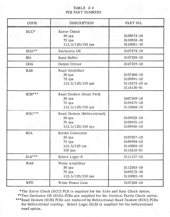
Typical Outline and Installation drawings are provided, in the drawing section of this techI1ical manual and in the TapeTransport manuals. Figure 2-1 shows typical printed circuit board assembly (PCBA) locations for 7-track and for 9-track Data Electronics. Mnemonic designations, as shown on the Logic Diagram, are provided. Table 2-2 lists the coded designation which appears on the ejector tab of the PCBA's and provides the part num-bers according to basic tape speeds.
2-6. CABLING.
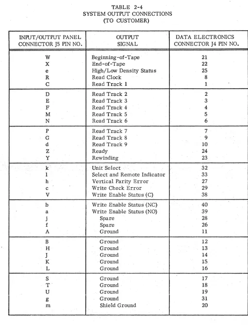
Cabling diagrams for TM-7211, TM-9211 and TM-1l211Tape Memory Systems are supplied in Section VIlof this manual. The TM-11211 diagram is also used for TM-l2211 systems. Inputs to the system and outputs from the system are connected to the Data Elec'" . tronics via the Connectors on the Input/Output Panel as shown in Tables 2-3 and 2-4,
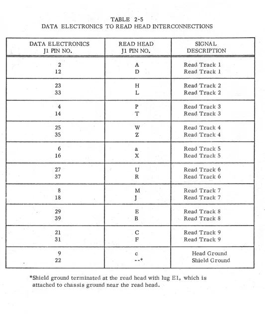
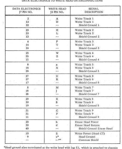
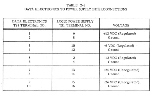
respec-tively. These inputs and outputs supersede those listed in the Tape Transport manual. Con-nections from the read heads are shown in Table 2 -S and conCon-nections to the write heads in Table 2-6. Table 2-7 lists connections to the Tape Transport. Table 2-8 lists connections to the Logic Power Supply. Tables 2-3 through 2-8 are located at the end of this section.
2-7. INPUT SIGNAL REQUIREMENTS.
2-8. INPUT SIGNAL VOLTAGE LEVELS.
The following signal voltage levels apply to all input signals (the input impedance
is 2300±115 ohms retUrned to-3. 8 volts. . . .
TRUE Level: -12 (+3, -13) volts
FALSE Level:. 0.00 ±1. 25 volts
I
NOTE .,
When non -standard input levels are provided, special Input Buffer PCBs .. and wiring changes are required.
2-9. INPUT SIGNAL TIMING.
In the following description of input signal timing, transition times are measured from the lO-percent pOint to the 90-percentpoint. Signal duration is measured from the 90-percent point of the leading-edge transition to the lO-percent point of the trailing-edge transition.
[image:11.613.53.586.36.784.2]TABLE 2-2 PCB PART NUMBERS
.. CODE ... , DESCRIPTION PART NO.
'.
ECC* Error Check
36ips 3109872-10
75 ips 3110558-10
112.5/120/150 ips 3110031-10
EOA** Exclusive OR 3107274-10
lEA Input Buffer 3107258-10
ODA Output Driver 3107259-10 .
RAB Read Amplifier
36 ips 3107266-10
75 ips 3109991 dO
112.5/120/150 ips 3110273,..10 or
3118138 -01
RDB*** Read Deskew (Read Fwd)
36 ips 3t07269-1O
75 ips 3109475-10
112.5/120/150 ips 3110004-10
' - - - - . -.~~~~~.~ c'···
RDC*** Read Deskew (Bidirectional)
36 ips 3109932-10
75 ips 3109935-10
112.5/120/150 ips 3109936-10
SGA Strobe Generator
36 ips 3107057-10
75 ips 3109994-10
. 112.5/120 ips 3110003-10
150 ips 3118218-01
SLB*** Select Logic-B 3111157-10
WAB Write Amplifier
36 ips 3112363-10
75 ips 3109572-10
112.5/120/150 ips 3110002-10
WPD W rite Power Gate 3107268-10
*The Error Check (ECC) PCB is supplied for the Echo and Rate Check option. **Two Exclusive OR (EOA) PCBs are supplied for the Vertical Parity Check option. ***ReadDeskew (RDB) PCBs are replaced by Bidirectional Read Deskew (RDC) PCBs
for bidirectional reading. Select Logic (SLB) is supplied for the bidirectional read option.
[image:12.615.13.558.35.731.2]2-10. Write Data. (See Figure 2-2.) A minimum interval of 1.5 Ilsec is required between the 90-percent pOint of the Write Data leading-edge transition and the lO-percent point of the next Write Strobe leading-edge transition.
A minimum interval of 1. 5 Ilsec is required between the 90-percent point of the Write Strobe trailing-edge transition and the lO-percent of the next Write Data leading-edge transition.
To write a series of ONE 'St the Write Data input may be held at the TRUE level for
the entire se:r;ies.
2-p. Write Strobe. (See Figure 2-2.) The Write Strobe leading (and trailing) edge
transition time shall not exceed 1. 5 Ilsec.
The Write Strobe TRUE state mUst coincide with the Write Data TRUE (or FALSE) state for at least2llsec.
2-12. Write Reset. The Write Reset leading (and trailing) edge transition time shall not .
exceed 1. 5 Ilsec.
The Write Reset signal must remain at the TRUE level for at least 1. 5 psec.
The Write Reset signal is used towrite the ~ongitudinal check character (Lee) at
. the end of each block of data. The LCC resets the NRZl write register.
A minimum interval of 106 Ilsec/ data transfer frequency is required between the
90-percent point of the Write Reset trailing-edge transition and. the lO-percentpointofthe next Write Strobe leading-edge transition.
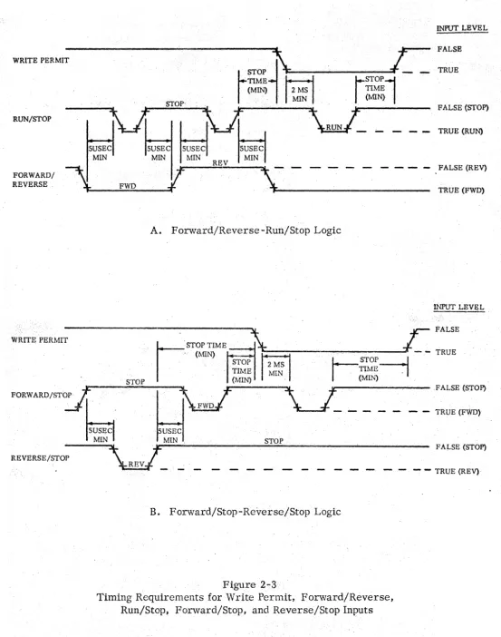
2-13. Wrjte Permit .. (See Figure 2-3.) The Write Permit leading (and trailing) edge
transition time shall not exceed 5 Ilsec.
The Write Permit level shall notbech~nged While the tape is in motion.
Write Permit should be at the FALSE level during Reverse and Rewind operations.
2-14. Read Permit. The Read Permit leading (and trailing) edge transition time shall not
exceed·S·l.lsec.
WRITE 'DATA
WRITE 'STROBE ,
.' STOP
"90% 10%
-
-
-
-
-'"---.;..---'
1.5
1.5
2.0 1.5 1.5SEC USEe USEC SEC USE
MIN MAX .MIN MAX MIN
INPUT
LEVEL
FALSE
TRUE
FALSE
_ ...;. _ _ TRUE
...
_ START TIME (MIN) ~ _ _ _ _ ...:. _ _ _ _ _ . _ _ FALSERUN COMMAND*/STOP
90% RUN COMMAND
*
Rl.}n Command is ItUIi1n
Fwd/Rev-Run/Stop logic systems andForward or Reverse in Fwd/Stop-Rev/Stop logic systems.
Figv.re2.,.Z
2·1S.HI/LO Density. The HI/LO Density leading (and trailing) edge transition time shall be S jlsec maximum; High density is selected by a TRUE level. The high/low density line
selects the appropriate timing read circuits.
('NOTII
This signal is normally supplied from the tape transport Operator Control Panel.
2 .. 16. Odd/Even Parity. The Odd/Even Parity leading (and trailing) edge transition time
shall not exceedS jJsec. Odd parity is selected by a TRUE, leveL The Odd/Even Parity line is used to select odd or even Read Vertical Parity check.
2·17. Forward/Reverse~ The Forward/Reverse leading (and trailing) edge transition time
shall not exceed S jJsec. (See Figure 2-3A.) The Forward mode is active when this line is at the TRUE level. Forward/Reverse transitions shall not occur while the tape is in motion.
A minimum interval oiS jlsec is required between a Forward/Reverse transition and the Run/Stop transition.
. .... ,.-.." ;".
~
Write Permit should be at the FALSE level when tape is moving in the Reverse direction.
2-18. Run/Stop. The Run/Stop leading (and trailing) edge transition time shall not exceed
Sjlsec. (See Figure 2-3B.) A TRUE level on this line sets the transport in the Run mode.
A minimum interval of 5 jJsec is required between the Forward/Reverse transition
and the Run command.
A minimum interval of 2.0 ms is required between a Write Permit transition and
a Run command.
A minimum interval equal to the stop time (to allow tape motion to stop) is required between the 90-percentpoim of a Stop command transition and a Write Permit transition.
INPUT LEVEL
FALSE WRITE PERMIT
r
STOP1~'-""'-.
_ _ _ _ _ _ _ _ _1-RUN/STOP
5USEC MIN
...
~~
...
~ r~~~1
STOP
I
;,,;;~
I
.
(MIN) ...I+---tU~
W--5USEC MIN
SUSEC SUSEC
MIN MIN
REV
TRUE
FALSE (STOP)
TRUE (RUN)
FORWARD/
REVERSE
't,-,,-~FWD ~r\-
- - -
---- FALSE (REV)
TRUE (FWD)
A. Forward/Reverse-Run/Stop Logic
INPUT LEVEL
A
L
FALSEr-5T~~~WE ~;dl ~r-~-~-s'-· ~I----I""
..
""-.-.-~-T-:i-~-.
_-..J:, - -
TRUESTOP
I .. .
I
~IN).
(MIN)WRITE PERMIT
)p.
f
"\ . . t
\
;-....---
FALSE (STOP)FORWARD/ST':i
I ·
~.·U··SE.c.1 ~
- - - TRUE (FWD)~
MIN MIN . STOPREVERSE/STOP ---.t~.. . . . . .. .
.
. •FALSE (STOP)
REV _ . _ . _ _ _ _ _ _ _ _ _ _ _ _ _ _ _ TRUE (REV)
B. Forward/Stop-Reverse/Stop Logic
Figure 2-3
[image:16.626.7.561.46.748.2]2-19. Forward/Stop (Option). The Forwaxd/Stop leading (and trailing) edge transition time shall not exceed 5llsec. (See Figure 2-3B.) The Forward mode is active when this line is at the TRUE level.
A minimum interval of 2.0 ms is required between a Write Permit transition and a Forward command.
A minimum interval equal to the stop time (to allow tape motion to stop) is required between the 90-percent point of a Stop command transition and a Write Permit transition.
2-20. Reverse/Stop (Option). The Reverse/Stop leading (and trailing) edge transition time
shall not exceed 5llsec. (See Figure 2-3B.) The Reverse mode is active when this line is at the TRUE level. A minimum interval equal to the stop time (to allow tape motion to stop) is required between the 90-percentpoint of a stop command transition and a Write Permit tran-sition.
Write Permit should be at the FALSE level when tape is moving in the Reverse direction.
2-21. Rewind~· The Rewind leading (and trailing) edge transition time shaH not exceed.5
Ilsec. The Rewind signal shall remain at the TRUE level for at least 5 Ilsec. Rewind opera-tion is initiated by the negative-going transiopera-tion.
2-22. Rewind and Lockout. The Rewind and Lockout leading (and trailing) edge transition
time shall not exceed 5 Ilsec. The Rewind and Lockout signal shall remain at the TRUE level
for at least 5 Ilsec. Rewind and lockout operation is initiated by the negative -going transition.
2-23.
2-24.
OUTPUT SIGNAL CHARACTERISTICS.
OUTPUT SIGNAL VOLTAGE AND CURRENT LEVELS~
TRUE Level: -11.5 (+2.5, -0.5) volts; 5 ma maximum from the load
FALSE Level:. 0.00:t1. 25 volts; 5 rna maximum to the load
I
NOiE·
When non-standard output levels are provided, special Output Driver PCBs and wiring changes are required.
OUTPUT SIGNAL TIMING •
In the following descriptiono! outpu(signal timing, transition times are ;measured
from the 10~percent point to the 90~percent point~ Signal duration is measured from the
90-percent point on the leading edge t:rans iti on to the 10.:.percentpoint on the tratling edge transition. Maximum leading edge displacement between Read Data, Read Clock, and Vet1:icalParityError outputs i80;,3 j.lsec maximum.
2-26. Read Data. The Read Data leading edge transition time is 0.30psec maximUm.
The trailing edge transition time is 0.30 Ilsec. Signal duration is from 0.9 Ilsecminimum to 1. S Ilsecmaximum.
2-27. Read Clock. The Read Clock leading edge transition time is. 0.30 Ilsec maximum.
The trailing edge transition .time is 0.30 Ilsec. Signal duration is from 0.9 Il sec minimum to 1. S Ilsee maximum.:
2-28 ... '; Vertical Parity Error (Option). The Vertical Parity Error lea<iing edge transition time is 0.30 Ilsec maximum. The trailing edge transition time is 0.30 Ilsec maximum. Signal duration is .from 0.9 Ilsec minimum to 1. S Ilsec maximum.
2
~
29.VI
rite Check Error .( Option) . The Write Cheek Error leading edge transItion time.is O. 30p.sec:: maximum~ The trailing edge transition time is 0.30p.sec maximum. Signal .
duration is fromO.S Ilsec mininium to S.3psec maximum.
2-30. . Write Enable Status. Three lines are provided to indicate the state of the write
permit relay on the Data Electronics Write Power GatePCBA • When a file -protect condition· ., exists, the write permit relay is deenergiz;ed and the Write Enable Status (C) line is con-. neeted to the Write Enable Status (NCr line. When a write enabie condition exists, the write permit relay is energized and the.Wtite Enable Status (C) line is connected to the Write Enable Status (NO) line.
2~31. TAPE TRANSPORT STATUS OUTPUTS.
Tape transport status output levels are -ll.S (+2.S, -0.5) volts (S ma maximum
frolILthe loa.d)andO. 00 ±1. 25 volts. (S mt;l. maximum to the load) for TRtJEand
1?
ALSE,respec-tively' unless otherwise indicated. Thestafus outputs are active in the remote mode only.
2-32. Beginning-otc-Tape (BQT). A.TRUE level on the BOT line indicates that the BOT tab
2-33. End-of-Tape (EOT). A TRUE level on the EOT line indicates that the EOT tab is being sensed by the photo sense assembly.
2-34. High/Low Density Status. The High/Low Density Status line acknowledges the
density select level. A TRUE level indicates that high density has been selected. A FALSE level indicates that low density has been se~ected.
2 -35. Ready. A TRUE level on the Ready line indicate s that all tape transport interlocks are closed and the transport is ready for remote operation.
2-36. Rewinding. A TRUE level on the Rewinding line indicates that the rewind operation
is being performed.
2-37. Unit Select. A TRUE level on the Unit Select line indicates that the tape transport
has been selected by a TRUE level at the Select input (when a single tape transport is used, the Select line is returned to -12 volts in the Data Electronics, thus providing a TRUE Select level at all times).
2-38. Select and Remote Indicator. This line is driven by a line driver returned to
ground. The line driver must be terminated with an indicator lamp returned to -12 volts (this is normally done by an indicator lamp in the Operator Control Panel of the Tape Trans-port). When so terminated, the line driver output is 0.0 ±1. 5 volts when the Unit Select status line is at the TRUE level; the line driver output is 125 ohms returned to ground when the Unit Select status line is at the FALSE level.
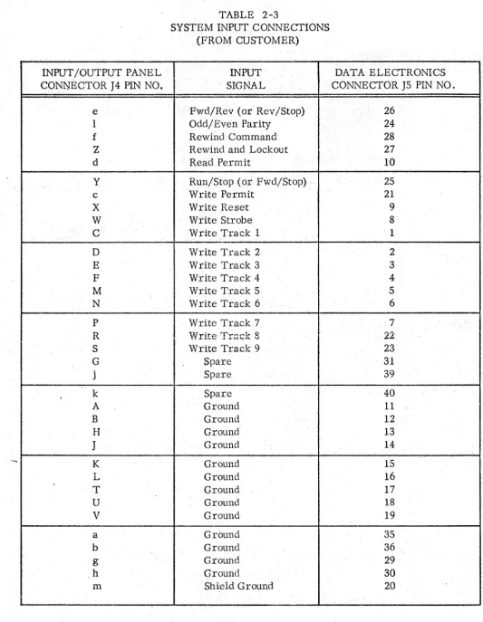
INPUT/OUTPUT PANEL CONNECTOR J4 PIN NO.
e 1 f Z d Y c X W C D E F M N P R S G j
, k
A B H
J
K L T U V a b g h mTABLE 2-3
SYSTEM INPUT CONNECTIONS (FROM CUSTOMER)
INPUT SIGNAL
Fwd/Rev (or Rev/Stop) Odd/Even Parity
Rewind Command Rewind and Lockout Read Permit
Run/Stop (or Fwd/Stop) .. Write Permit
Write Reset W rite Strobe Write Track I
W rite Track 2 W rite Track 3 Write Track 4 Write Track 5 W rite Track 6
Write Track 7 Writ.:> o ... _ 'r.,.."".], .... .Lt...4.'-.t'- V Q
W rite Track 9 Spare Spare Spare Ground Ground Ground Ground Ground Ground Ground Ground Ground Ground Ground Ground Ground Shield Ground
DATA ELECTRONICS CONNECTOR J5 PIN NO.
[image:20.630.10.544.27.714.2]INPUT/OUTPUT PANEL CONNECTOR J5 PIN NO.
W X e R C D E F M N P G d Z Y k I h c V b a j f A B H
J
K L S T U g mTABLE 2-4
SYSTEM OUTPUT CONNECTIONS (TO CUSTOMER)
OUTPUT SIGNAL
Beginning-of-Tape End-of-Tape
High/Low Density Status Read Clock
Read Track 1
Read Track 2 Read Track 3 Read Track 4 Read Track 5 Read Track 6
Read Track 7 Read Track 8 Read Track 9 Ready
Rewinding
Unit Select
Select and Remote Indicator Vertical Parity Error
Write Check Error Write Enable Status (C)
Write Enable Status (NC) Write Enable Status (NO)
Spare Spare Ground Ground Ground Ground Ground Ground Ground Ground Ground Ground Shield Ground
DATA ELECTRONICS CONNECTOR J4 PIN NO.
[image:21.615.60.572.41.710.2]00
TABLE 2-5
DATA ELECTRONICS TO READ HEAD INTERCONNECTIONS
DATA ELECTRONICS READ HEAD SIGNAL
Jl PIN NO. Jl PIN NO. DESCRIPTION
2 A Read Track 1
12 D Read Track 1
23 H Read Track 2
33 L Read Track 2
4 P Read Track 3
14 T Read Track 3
25 W Read Track 4
35 Z Read Track 4
6 a Read Track 5
16 X Read Track 5
27 U Read Track 6
37 R Read Track 6
8 M Read Track 7
18
J
Read Track 729 E Read Track 8
39 B Read Track 8
21 C Read Track 9
31 F Read Track 9
9 c Head Ground
22
--*
Shield Ground [image:22.624.21.555.31.669.2]TABLE 2-6
DATA ELECTRONICS TO WRITE HEAD- INTERCONNECTIONS
DATA ELECTRONICS WRITE HEAD SIGNAL
J7
PIN NO. J2 PIN NO. DESCRIPTION2 A Write Track 1
12 D Write Track 1
22 .'
--
Shield Ground 123 H Write Track 2
33 L Write Track 2
13
--
Shield Ground 24 P Write Track 3
14 T Write Track 3
24
--
Shield Ground 325 W Write Track 4
35 Z Write Track 4
15
--
Shield Ground 46
a
W rite Track 516 X W rite Track 5
26
--
Shield Ground 527 U W rite Track
6
37 R . Write Track 6
17
'--
.. Shield Ground 68 .M Write Track 7
18 J Write. Track 7
,
28--
Shield Ground 729 E Write Track 8
39 B W rite Track 8
19
--
Shield Ground 821 C Write Track 9
31 E Write Track 9
11
--
Shield Ground 920 b Erase Head Power
30 d Erase Head Return
40
--
Shield Ground Erase Head10 S Write Power (Head CT)
9 c* Head Ground
--
--** Common ShieldI I I
*Head ground also terminated at the write head with lug E1, which is attached to chassis ground near the write head.
**Common shield terminated at the write head with lug E2, which is attached to terminal E2 near the write head.
I
[image:23.613.57.571.48.673.2]. . TABLE2-7 .
DATA ELECTRONICS TO TAPE TRANSPORT INTERCONNECTIONS
DATA ELECTRONICS SIGNAL TM-7/TM.,.9
J6PIN NO. DESCRIPTION . }10 PIN NO.
\ .
6
'.Begi:h.ning-:"of-Tape (-) 6
8 End-ai-Tape (-) 8
1 Forward/Reverse (-/+)* 1
7 High/Low Density (-/+) . 7
19 High/Low Density Status (-/+) 19
10 Readyk) 10
4 Rewind arid Lockout (-) 4
3 Rewind Command ( -) 3
9 Rewinding ( ... :) 9
2 Run/Stop ( c/+)** 2
5 Select (-) 5
18 Select and Remote Iridicator (+) 18
14 Unit Select ( -) 14
15 Write Enable Switch/Rela.y (C) 15
16 Write Enable Switch/Relay (NC) . 16
17*** Write Enable Switch/Relay (NO) 17
11 Ground 11
12 Ground 12
13 Ground 13
20 Shield Ground 20
*Reverse/Stop (-/+) when Fwd/Stop-Rev/Stop logic is supplied.
**Forward/Stop (-/+) when Fwd/Stop-Rev/Stop logic is supplied
***Pln 17 of J6is returned to,gro1:rnd in the Data Electronics
TM-11/TM.,.12 CONTROL . ELECTRONICS
J4 PIN NO.
11 12 14 7 3
:
2 9 8 1 15
4 6 5 18 17
TABLE 2-8
DATA ELECTRONICS TO POWER SUPPLY INTERCONNECTIONS
DATA ELECTRONICS LOGIC POWER SUPPLY
TS1 TERMINAL NO. TSI TERMINAL NO. VOLTAGE
1 6 +12 VDC (Regulated)
2 8 Ground
3 10 -6 VDC (Regulated)
4 12 Ground
5 2 -12 VDC (Regulated)
6 4 Ground.
7 13 +24 VDC(Uriregulated)
8 14 Ground
9 15 -24 VDC (Unregulated).
10 16 Ground
[image:25.613.66.579.54.377.2]3-1. INTRODUCTION.
SECTION III
,OPERATIDN
This section briefly describes the operation of the Data Electronics.
3-2. OPERATING MODES.
The Data Electronics is capable of operating in three different modes:. ·write check, write only, and read only. The operating mode is determined by the level of the Read Permit and. Write Permit input Signals.
3-3. WRITE CHECK MODE.
In tile Write Check Mode, information is read immediately after it is written. To
operate in the Write Check Mode, Write Perinit and Read Permit inputs must be TRUE~
.3-4. WRITE ONLY MODE •
. In the Write Only Mode, information is written but reading does not occur. To
. operate in theWri,te Only Mode,· Write Permit illput must be TRUE and Read Permit.input .. must be FALSE.
3;..5·. READ ONLY MODE~
In the Read Only Mode, information is read. but writing does not occur. To operate .in the Read Oilly Mode. Read Permit input must be TRUE and Write Permit input must be FALSE.
3-6. WRITE SIGNAL CONDITIONING.
Writing of data is accomplished on seven (or nine) tracks. In the following
description of write signal conditioning. the operation of only one track is discussed~ Each
3-7. WRITE DATA. (See Figure 3'-1.)
Data is written when the Write Data input is strobed through an AND gate by the Write Strobe and fed, via an OR gate, to the Write Deskew single-shot delay. Write Head gap-to-gap static skew is compensated for by the single-shot delay. The deskewed Write Data signal is fed to the write register. Write Permit is comprised of the ANDed Write Permit and Run inputs. The write register controls the direction of current flow in the write head.
3-8. WRITE POWER.
Whenthe Write Permit signal is TRUE and a Write Enable Ring is in-place, power is supplied to the Write and Erase Heads through the Write Power Gate.
3 -9. WRITE RESET.
The Write Reset signal is ANDed with the Set status output of the NRZ Write Register and is then fed to the NRZWrite Register flip-flops via the OR gate and the single-shot delay. The "VXrite Reset line is used to write the Longitudinal Check Character (LCC) at the end of each block of data. The LCG is used to reset the NRZ register, resulting in an even number of flux reversals (ONEs) in each track of the block.
TEST DESKEW
1.[
L.
WRITE PATA
1I
Jl..
(AC SET AND RESETWRITE StROBEL[
..
WRiTE BY T~AIUNG EDGE) .~ WRITE DATAAND OR DESKEW
I t . .
NRZIr+
55 REGISTER WRITE WRITE HEAD-
FF I--WRITE RESET1I
-1I
(DC RESET WHENWRITEPERMIT OR
AND RUN IS FALSE)
r
WRITE REGISTER FF SET STATUS .... RUN...
WRITE PERMIT AND RUN AND
WRITE PERMIT
I
WRITEWRITE PERMIT POWER
WRITE
WRITE WRITE ENA8LE POWER GATE ERASE POWER ERASE
ENA8lE HEAD
SWITCH
Figure 3-1
Read Signal Conditioning, Block Diagram
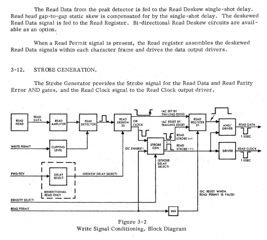
[image:27.624.19.567.84.739.2]3-10. READ SIGNAL CONDITIONING.
Reading of data is accomplished on seven (or nine) tracks. In the following description of read signal conditioning, only one track is discussed.
3-11. READ DATA. (See Figure 3-2.)
The signals from the Read Head are amplified by the Read Amplifier and fed to the peak detector circuit on the Read Deskew PCBA. The peak detector generates positive pulses, corresponding in time to the peaks of the analog Read Head signals. The peak detector clip-ping level is established as a function of Write Permit.
The Read Data from the peak detector is fed to the Read Deskew single-shot delay. Read head gap-to-gap static skew is compensated for by the single-shot delay. The deskewed Read Data signal is fed to the Read Register. Bi-directional Read Deskew circuits are avail-able as an option.
When a Read Permit signal is present, the Read register assembles the deskewed Read Data signals within each character frame and drives the data output drivers.
3-12. STROBE GENERATION.
The Strobe Generator provides the Strobe signal for the Read Data and Read Parity Error AND gates, and the Read Clock signal to the Read Clock output driver .
..Jl.
READ HEAD
READ
DATA READ ! . . . PEAK
AMPLIFIER r--v DETECTOR CLOCK OR
CAC SET BY TRAILING EDGE) (AC RESET BY
TRAILING EDGE)
RE'g~~ER
Lr--...;...,
_W ... RI_TE_P.;...ER.-.M_IT _ _ _ ... CLIPPING L...;.. _ _ ...
• LEVEl r
FWD/REV
DENSITY SHECT
r - - - ,
I
II
DelAY SELECT
I
I
I
I
L
81DIRECTIONALI
R~O~_J
CDESKEW DelAY SElECT)
1f
,
r- READ' - - - - 1 · L!i' STROBE C-)
I I
STROBE I i-i READ CDC ENAB~ GeN U L STROBE (+)
(STROBE DELAY
SElECn
FF
~~~----~---~~---~WINV~----~
~~
1
EJ
Figure 3-2
Write SignalConditiorting, Block Diagram
AND/ DRIVER
DRIVER
CDC RESET WHEN READ PERMIT IS f AlSEl
READ DATA
1f
1 lISEC
READ CLOCK
1f
[image:28.615.46.597.224.718.2]3-13. ERROR CHECKING.
3-14. VERTICAL PARITY CHECK.
The vertical parity check circuits generate an Error signal when the parity of the read register does not correspond to the status of the Odd/Even Parity input. In the Read Only Mode, the Error output is provided at the Vertical Parity Error output. In the Write Check Mode, the error indication is provided at the Vertical Parity Error output and at the '\Yrite Check Error output
3-15. RATE CHECK.
The rate check circuit generates a Write Check Error output when the time interval between successive characters is below a design threshold.
3-16. ECHO CHECK.
In ORed Clock systems, at least one Write Amplifier flip-flop must change state after each Write Strobe. The echo check circuits generate a Write Check Error output when none of the Write Amplifiers change state after receipt of a Write Strobe.
READ STROBE (+)
n
1 USEC
READ DATA
.,
4.
AND/lS
VERTICAL PARITY ERROR. II>READ PARITY ERROR DRIVER
ODD/EVEN PARITY
PARITY. SELECT CHECK
r
~
VERTICALPARITY
lS
AND ERROR
1 USEe
1,[
RATElSY
1.f.
1.f
READ STROBE (-) RATE ERROR PULSE WRITE CHECK
CHECK
..
OR GEN ERRORr+
AND/~
DRIVER
U
ECHO
n.
.
ECHO
lS
1 USECI ~
ERROR
lJf
ECHOWRITE STROBE CHECK
"
WRITE PERMIT AND RUN
t
IDC RESET WHEN WRITE PERMIT OR RUN IS FALSE) WRITE PERMITFigure 3-3
Error Check Circuits, Block Diagram
[image:29.615.16.566.74.750.2]·
s'aCTIONIV
THeORY OF OPERATIDN
4-1. INTRODUCTION.
This section includes the theory of operation of the Data Electronics and an intro-duction to the graphic symbols used in the logic diagrams.
4-2. LOGIC DIAGRAM.
The Data Electronics logic diagrams in Section VII illustrate the logic functions in the data card cage . Use of the logic diagrams will facilitate the rapid diagnosis and localization of equipment malfunctions.
4-3. LOGIC LEVELS.
Most Data Electronics signals are binary level. Where binary levels are'used; one
of the two levels is a 0.0 ±O.5 volt level. The second level is generally a -6 volt level. In
some circuits, -12 volt, +6 volt, or +12 volt levels are used. When the binary signal levels
are 0 and -6 or -12, the 0 volt level Is relatively high and is therefore termed positive (+) .
. ' When the binary signal levels are 0 and +6 or Oand +12, the 0 volt leve~ is relatively low and
is therefore termed negative ( -).
Signal callouts in the Data Electronics logic drawing (Section VII) show the TRUE (active state) of the signal. Write Permit (-) indicates that Write Permit is TRUE when the Write Permit signal is relatively low. ReadStrobe (+)indicates that·R.ead Strobe Is TRUE
when the Read Strobe Signal is relatively high. Run/Stop (-I+) indicates Run (-) is TRUE
when the signal is relatively low and Stop (+) is TRUE when the signal is relatively high.
4-4. LOGIC ELEMENTS.
4-5. Identification. Identification of a logic element is accomplished by the graphic
symboLand the notation within the symbol. (See Figure 4 -1.) The mnemonic de signation
identifies the PCB nomenclature. The bottom notation identifies the physical location of the PCB in the card cage .
4.,.6. State Indicators. A state indicator (small circle) atthe input to any logic element
10
--4-2
a
AMPLIFIER
c
NOR
9
I~~
SGr::
88
e
GENERAL
Figure 4-1 Logic Symbols
AC SET)
-DC RESET) 26_
""
AC. RESET) 24
RD A2
b
FLIP-FLOP
32
1...30
....
d
[image:31.615.13.537.108.714.2]4-7 .. SIGNAL F LOW DIRECTION.
Direction of signal flow is indicated by logic symbol orientation. Inputs to a circuit are from the left and outputs are from the right.
4-8. LOGIC SYIvlBOLS.
4-9. Amplifiers. The triangular symbol represents either a current or a voltage amplifier.
The amplifier may have one or more stages and mayor may not produce gain or inversion. Figure 4-1a represents an Input Buffer circuit. The presence of state indicators (small
circles) at input pin 10 and output pin
9
signifies that inversion has not taken place .. 4-10. Flip-Flops. The rectangular symbol, Figure 4-1b, denotes the flop. The
flip-flop is a device which stores a single-bit of information. Two or more inputs may be used to Set or Reset the flip-flop to produce two simultaneous outputs, low level and high level. The outputs of the flip..;flop are always shown in the set state.
4-11. Gate Circuits. Gate circuits are represented as shown in Figures4-1c and 4-2 and
may have one or more stages that mayor may not produce gain or inversion. The presence of state indicators at the inputs or at the single output indicate whether ornotipversion has. taken place.
A two-input AND gate, Figure 4-2a. signifies that two relatively low levels
co-inc~dental at the inputs (pins 11 and 12) will produce a relatively low output •. Conversely, Figure 4-2c denotes a two-input AND gate where two relativelyhigh levels present coinci..; . dentally at the inputs will produce a relatively high output.
Figure 4-2e represents a two-input NAND (NOT-AND) gate that produces inversion. When two relatively high levels are present coincidentally at the inputs (pins 11 and 12) a relatively low level output is produced. Conversely, in Figure 4-2g, two low levels coinci-·· dental at the inputs will produce a relatively high level output frorn the NAND gate.
Two-input OR gates, Figure 4-2b and 4-2d, produce an output when a signal is present at any of the inputs. In Figure 4-2b. a relatively high level at either of the inputs Will produce a high level output. In Figure 4-2d, a relatively low level at either of the inputs will produce a relatively low level output.
LOGIC SYMBOLS
AND
~
:;.)--a
I
)-c
NAND
12 ..
I
OD~
~11
B13e
_3S~
"?
B 12
9
4-4
OR
--,·1
~:>
b
W
18_~
.
d
NOR
d
::)-f .
[image:33.615.12.554.44.719.2]):2:>-h
Figure 4-2 Gate Circuits
TRUTH TABLES
INPUT 1 INPUT 2 OUTPUT
LOW LOW LOW
LOW HIGH HIGH
HIGH LOW HIGH
HIGH HIGH HIGH
LOW LOW LOW
LOW HIGH LOW
HIGH LOW LOW
HIGH HIGH HIGH
INPUT 1 INPUT 2 OUTPUT
..
LOW LOW I-UGH
LOW HIGH HIGH
HIGH LOW HIGH
HIGH HIGH LOW
LOW LOW HIGH
LOW HIGH LOW
HIGH LOW LOW
Figure 4-1c represents a three-input'NOR gate. A relatively low input at any of the three inputs will cause a relatively high level at the output. The absence of pin numbers and the dashed lines indicate that the preceding and following logical elements are on the same printed circuit board.
3-INPUT NOR GATE TRUTH TABLE
INPUT 1 INPUT 2 INPUT 3 OUTPUT
High Low Low High
High High Low High
. High High High Low
Low High High High
Low Low High High
Low Low Low High
.'
4-12. Exclusive OR Gates. Exclusive OR gates are used in the optional error detection
circuits. Figure 4~ld represents the Exclusive OR gate. A relatively high level output
appears only when the inputs are dissimilar.
EXCLUSIVE OR GATE TRUTH TABLE
INPUT 1 INPUT 2 OUTPUT
High Low High
Low High High
High High Low
Low Low Low
[image:34.620.47.580.35.694.2]4-14. WRITE LOGICAL SEQUENCE.
4-15. INPUT BUFFERS.
Input buffers are used to provide isolation and supplypoW'er gain to the input signals.
4-16. WRITE DATA .
. ATRUE (low level) Write D<;tta signal at pin 12 of the write amplifier data input AND gate enables the AND gate., A Write Strobe pulse coincidental with the TRUE Write Data signal produces a going pulse at the output of the AND gate. The negative-going pulse is applied through a NOR gate to the input of the Write Deskew single-shot delay. The positive-going p'ulse from the NOR gate triggers the single-shat delay, which produces a positive""going pulse. The width of the single-shot delay pulse is adjustable and is set to compensate for the gap-to-gap misalignment (static skewrof the write heads.
The negative-going trailing edge of the Single-shot delay pulse triggers the Write Register flip-flop and the flip-flop changes state. When the flip-flop changes state,the direction of current flow through the write head is reversed, which causes the polarity of the head magnetic ,flux to reverse. The flux polarity change is impressed on the tape and
is interpreted as a logical ONE during the read function. .
4-17. WRITE RESET.
The' Write Reset signal is used to reset the Write Register flip-flops and to generate
the LPC character. The Write Registerfiip-flopsare in t1i.e reset $ tate at the start of each
block of w'rit:edata. If im odd nurriber of data bits are written on anyone track, that Write
Register flip -flop is in the set state after the lastdata bit of the block is written. A low level status signal from the set flip,..flop enable s the Write Amplifier reset AND gate. The Write Reset puiseproduces anegative::"going pulse at the output oithe resetAND gate. The negative-going pulse is applied through the NOR gate to the input of the Write Deskew single;..
shot delay and causes a ONE to be written as previously described for the Write Data input. 'The Write Register flip..:f1op is then iuthe reset state.
The reset of the flip-flops generates the Lee which provides an even number of data bits in each track of a data block.
4-18. WRITE REGISTER DC RESET.
The NAND gate is located on the Strobe Generator PCB. When either the Write Permit signal or the Run/Stop (or Fwd/Stop) signal is at the.FALSE (high) level, the output of the NAND
gate is at the low level. The low level output from the NA~D gate DC resets the Write
Register flip-flops and holds the flip-flops in the reset state.
4-19. TEST DESKEW.
A negative-going Test Deskew pulse train applied at Test Point. TP1 of the Data Elec-tronics is applied through the Write Amplifier NOR gates to the inputs of the Write Deskew single-shot delays. The pulses cause all ONEs to be written as previously described for the Write Data input. The Test Deskew input is used during off-line Write Deskew adjustment procedures. The Write Reset and the Write Strobe inputs must be FALSE when the Test Deskew input is used.
4-20. WRITE HEAD POWER.
Write Head Power is fl;trnished by the Write Power Gate. When the Write Permit input is at the TRUE level and a write enable ring is in place in the file reel, +10 volt power is supplied to the write heads from the Write Power Gate PCB through pins 28, 29, and 30. The write power relay on the Write Power Gate PCB is energized when the write enable ring is sensed by the write enable switchassembly on the tape transport.
4-21. READ LOGICAL SEQUENCE.
4 - 22. READ PERMIT.
Read Permit TRUE enables the read strobe generator circuits. Read Permit FALSE, DC resets the read register flip-flops and holds the flip-flops in the reset state.
4-23. READ DATA •. (See Figure 4~3.)
Flux transitions (written ONEs) on the tape are sensed by the read heads as bipolar analog Read Data signals. The Read Data signals from each read head are amplified ina three-stage differential voltage amplifier on the associated Read Amplifier PCB assembly and then applied to a differential VOltage amplifier on the associated Read Deskew PCB assembly.
-r-
T ·A
.A\
.. ', .... ____
TRACK 1 READ AMPLIFIER OUTPUT8V I _ _ _ _ _ _ _ _ ... __ . ; .
-L~ I~
__ READHEADV
:
.
~l,---
STATIC SKEW* Iat
:A
....
-·---_r.
:
A ___
~iL~F~E:ES~TPUT
L
:
I
rv
I:
I I I
-::~
0
...
:1--__________ ...
0
'-....,1 _ _-I I I
TRACK 1 PEAK DETECTOR OUTPUT
OV
n
n
n·
TRACK 2 PEAKDETECTOR OUTPUT
-6V - - - t -... I.. - - - -... " ' - - - - -_ _ _ _ _ _ _ _ ... '
-I
_::~L...,..--'f
f
~r
I
OV - - - . . .
r---.
11"---_1
C--6V U---.rRAIUNG EDGE
U
L...J
SETS READ REGISTER fF
TRACK 1 READ DESKEW SS OUTPUT TRACK 2 READ DESKEW 55 OUTPUT
OV
---.U
-6V
u
u--OR CLOCK OUTPUT . .. FROM READ DESKEW 55
I I
ov
---""1
i// ____
DYNAMIC-6V ~ SKEW BAND
1
\IL'
I ,J
\iff
OR .. CLOCI( INPUTS TO
I .I'. STROBE GENERATOR
_:: ~~----t~
f
~
__
. _---.If
.~
L
DELAY SS OUTPUT READ STROBEI
I
+12V
--Il...
n
-6V -_---r"---~-
...
L ~=--_ 0.9 to 1.5 USEC ... _ _ _ _ _ _ _I
OV . ; ; . . . - - - ' - - - . . . - - - . '
'-6V
~C'.
-. _ .. -.. -'-. -T-R-A-IL-IN ... G-ED-C;-e----'Lf!
RESETS READ REGISTER FFJr---:-.,:
I
I
- 6 V - - - ' I
OV
,
OV ---i'~---~U~---,U
-12V I
,
,--DELAY ..-J
'~-1/2 fRAME TIME ~ I
*The read amplifier data outputs are caused by flux reversals on the tape which are sensed by the read heads. Flux reversals on the tracks are written COincidentally; the time displacement shown (read head static
skew) is caused by gap-to-gap misalignment of the read heads.
4-8
Figure 4-3 Read Deskew Timing
READ STROBE (+)
READ STROBE (-)
READ REGISTER FF
[image:37.615.23.544.11.726.2]The clipped analog Read Data signal is applied to the peak detector circuit which produces a positive-going pulse at the positive or negative peaks of the signal. The leading edge of the peak detector output pulse is coincident with the detected peak. The positive-. going pulse triggers the Read Deskew single-shot delay, which produces a negative-going
pulse. The width of the single-shot delay pulse is adjustable and is preset to compensate for the gap-to-gap misalignment (static skew) of the read head. Two pulse widths are set for bidirecti.onal read systems; the forward deskew pulse width is selected when the Forward/ Reverse (or Forward/Stop) input is TRUE, the reverse deskew pulse width is selected when the Forward/Reverse (or F.orward/Stop) input is FALSE.
The positive-going trailing edge of the single-shot delay pulse sets the Read Register
flip-flop and the Read Data output at pin 32 of the Read Deskew PCB goes to the TRUE (high)
level. The Read Data output is applied toone inpUt of a NAND gate driver circuit and enables . . .
the NAND gate. A Read Strobe (+) pulse coincidental with the TRUE Read Data signal
pro-duces a negative-going pulse at the outputof the NAND gate driver. The negative-going
pulse is a TRUE Read Data output representing
a
ONE sensed from the tape.The Read Register flip-flop is reset by the positive-going trailing edge of the Read Strobe (-) pulse.
4-24. READ STROBE.
.. The Read Strobe (+) and Read Strobe (-) pulses are generated on the Strobe Generator
PCB assembly. The positive-going trailing edge of each Read DeskeW Single-shot delay pulse
is coupled through an associated inverter driver stage to produce a negative-going ORClock
pulse. The OR Clock pulses are applied to one common input of an AND gate on the Strobe Generator PCB. The other input to the AND gate is the Read Permit Signal. When Read . Permit is at the TRUE (low) level, the OR Clock pulses are passed through the AND gate. The -first OR Clock pulse through the AND gate triggers the Read Strobe single-shot delay , which produces a negative-going pulse. The width of the single.,.shot delay pulse is adjust-able and is preset to approximately one-half the character frame time, less the read strobe pulse time. Two Single-shot delay pulse widths are preset: one for the high density packing
rate, the other for the low density packing rate . Selection of the pulse width is accomplished .
by switching circuits on the Write Power Gate PCB. When the HI/LO Density line is at the
low level, the High Density pulse width is selected. When the HI/LODensity line is at the
high level, the Low Density pulse width is selected.
The positive-going trailing edge of the Read Strobe Single-shot delay pulse is
coupled to a pulse generator circuit which then generates the poSitive-going Read Strobe (+)
pulse. The pulse width of the Read Strobe (+) pulse is approximately 1 microsecond. The
·Read Strobe (+) pulse is inverted through an inverter stage to produce the Read Strobe (-)
4-25. ERROR CHECK OPTIONS.
Error check options consist of Vertical Parity Check, Rate Check, and Echo Check. (Seethe Data Electronics Logic Diagram in Section VII.)
4-26. VERTICAL PARITYCHECK.
Vertical Parity is checked during both Read Only and Write Check Modes of operation by a continuous frame-by-frame check of the contents of the read register. A parity-select level from the customer selects either odd or even parity check. Odd parity requires an odd number of logical ONEs be recorded in every character frame. Even parity requires an even number of logical ONEs in every character frame. A Vertical Parity Error exists when an extra (or missing) logical ONE is detected.
Numerical values in parenthesis in the following circuit description refer to 9 -track systems. The Odd/Even Parity Select line and the complementary outputs of the Read Register flip -flops are applied to the inputs of the parity che'cking circuit on the Exclusive' OR PCB
assembly. Eight Exclusive OR gates are used for 7-track systems, nine for 9-track systems. Each gate compares two inputs and produces a high level output when the logic levels of the inputs are dissimilar. Seven (or nine) Read Data (-) lines from the Read Register flip-flops and the Odd/Even Parity Select line are applied t() four (or five) of the Exclusive OR gates. The outputs of the four gates are applied in pairs to the following two Exclusive OR gates, the outputs of which are compared by a single gate. The output of the single gate is compared in a final Exclusive OR gate with a fixed low level input (in 9-track systems, the output of the fifth input Exclusive OR gate is compared with the output of the single gate in the final Exclu-sive OR gate). The output of the final gate is ANDed with the Read Strobe (+) pulse in a NAND. gate driver. If a vertical parity error is sensed, a negative -going Vertical Parity Error pulse is produced at the output of the NAND gate driver and is transmitted to the customer via the system output connector.
4-27. RATE CHECK.
Rate Check is performed only during the Write/Check mode. A Rate error pulse is generated when the interval between successive Read Strobe (-) pulses decreases to
1
0.67 (tape speed in ips) (high bit packing density)
The Rate Check circuit is located on the Error Check PCB and operates in the following manner. (See Figures 4-4 and 4-5.) The Read Strobe (-) pulse triggers single-shot delay A which produces a negative -gOing pulse . 111e positive -~oing trailing edge of the single-shot delay A pulse triggers single-shot delay B, which produc'e,s'~' negative-going pulse. The next arriving Read Strobe (-) pulse retriggers single-shot'delay A and also is ANDed with the outputof single-shot delay B. If the Read Strobe (-) pulse and the output pulse from single-shot delay B are coincident, a rate error pulse is generated.
READ STROBE (-)
DELAY A
DELAY B
Figure 4-4
AND
..
...
RATEERROR
Rate Error Check, Block Diagram
READ
-u
STROBEC .... }
DELAY A· - - , .... _ _ ~J
DELAY B
u
THIRD READ STROBE· (-)
. PULSE OCCURRED TOO EARLY
r
ERROR PRODUCED. WHEN .RATE .. _________________ ~---~r1
.
ERROR
[image:40.612.86.592.126.725.2]4-28. ECHO CHECK.
An Echo output is generated by each·Write·amplifier whenever the amplifier changes
state and reverses the Write head coil current. The Echo output is
a
positive-going pulsederived from the induced EMF generated by the Write head inductance when the write head
coil current reverses. .
In ORed Clock systems, the data that is written must cause at least one head driver to change state in each frame. The Echo output of each Write amplifier is ORed with the· Echo outputs of all other Write amplifiers to generate an ORed Echo output. The ORed Echo
output occurs if any Writearriplifier changes state during the frame interval. If no ORed
Echo occurs during the frame, a malfunction in the Write circuitsis indicated and an Echo error pulse is generated by the EchO Check circuits.
The Echo error pulse is generated in the follOWing manner. (See Figures 4-6 and 4-7.) The Write Strobe triggers the Single-shot delay and the leading edge of the
single-. shot &~lay pulse sets the flip-flop. The Write Strobe holds the AND gate FALSE .for the
strobe duration to prevent any output from the AND gate during the period that the single-'shot. delay and flip.,.flop are going TRUE. The AND gate is also held FALSE by the single-shot delay pulse for the durat1onof its delay.· The Echo input must occur som.etime after the Write Strobe and within the duration of the Single-shot output. The Echo input resets the flip-flop.
If no Echo input occurs, .the flip-flop remains set at the end of the single.,.shot delay pulse
and the output of the AND gate goes TRUE, indicating an Echo Error. .
4-29. WRITE/CHECK ERROR.
The Vertical Parity Check output, Rate Check output, and Echo Check output are QRed together. The occurEmce of any error triggers a pulse generator circuit,which pro-duces. a negative-going 1 microsecond error pulse. The error pulse is ANDedwithWrite
. Permit. I f the Write Permit is TRUE, anegative-g-oingWrite Check .Error pulse is pro'"'
duced at the output of the AND gate driver and is transmitted to the customer via the system· output connector.
WRITE STROBE
ECHO
WRITE STROBE
DELAY
Flj·P.FlOP
u
AND --"'
-DELAY S
FF
ECHO
[image:42.613.69.559.29.729.2]AMP
Figure 4-6
Echo Check. Block Diagram
u
u
I
K~
_ _ - - - - ' ' - -_ _ _ _ _ _ _n
- - ' L..-_ _n·
ERROl
~ ERROR. NO ECHO FOR
ERROR.
"'---'1'-
~~~~END WRiTE STROBE---',
.5-1. INTRODUCTION.
SECTION V
MAINTENANCE
This section contains adjustment procedures and troubleshooting techniques for the Data Electronics. Tape Transport maintenance is included in the Tape Transport manual.
5-2. TEST EQUIPMENT.
Table 5-1 lists the required test equipment.
TABLE 5-1
REQUIRED TEST EQUIPMENT
RECOMMENDED TYPE
EQUIPMENT OR EQUIVALENT
Digital Voltmeter (DVM) Digitek 202-B
Master Tape . IBM
Oscilloscope Tektronix 535
Preamplifier Tektronix CA
Square Wave Generator Hewlett-Packard HP-211
5-3. ADJUSTMENT PROCEDURE.
5-4. GENERAL.
Note that adjustments are made by Ampex prior to the shipment of equipment.
Verify adjustments when components are either interchanged or replaced. If adjustments
are to be made off line, use Alternate Adjustment Procedure. (Refer to paragraph 5-14.)
An insulated-blade screwdriver is recommended for making adjustments to prevent accidental shorting of electrical components.
[image:43.618.46.586.78.761.2]5-5. SEQUENCE OF ADJUSTMENTS.
Tape transport and power supply adjustments must be verified before Data Electronics adjustments are made. Data Electronics adjustments shall be made in the following sequence.
1. Clipping Level
2. Preliminary Read Amplifier
3. Read Deskew
4. Write Check
5. Read Amplifier
6. Write Deskew
7. Read Strobe
S. Rate Error
5-6. Clipping Level. The bias setting adjustment on the Strobe Generator card
deter-mines the clipping level. In the Read Only Mode, the clipping level is at 20 percent. In the Write. Check Mode, the clipping level adjustment is at 40 perc