GPM AND GPM - Sol
ASSEMBLY AND TEST INSTRUCTIONS
~Processor
I
~TechiioIogy
Processor lec~'Corporation
6200HoIlisS~~T
{
~--GENERAL PURPOSE MEMORY MODULE GPM and GPM-Sol
ASSEMBLY and TEST INSTRUCTIONS
GPM Contents
SECTION TITLE PAGE
1 INTRODUCTION and GENERAL INFORMATION 1.1
1.2
Introduction . . . 1-1
General Information . · 1-1
1.2.1 1.2.2 1.2.3
Description . . . 1-1 GPM and GPM-Sol Version~ . . . • . . . 1-2 GPM Voltage Requirements, Typical . . . 1-4 1.3 Warranty and Replacement Information · . 1-4
1.3.1 1.3.2 1.3.3 1.3.4
Receiving Inspection . . . 1-4 Warranty Information . • . 1-4 Replacement Parts . . . 1-4 Factory Service . . . 1-5 2 ASSEMBLY
2.1 Parts and Components · 2-1
2.2 Assembly Tips . . . . • 2-1
2.3 Assembly Precautions · . 2-3
2.3.1 2.3.2 2.3.3 2.3.4 2.3.5
Handling MOS Integrated Circuits · 2-3 Soldering **IMPORTANT** . . .
Installing and Removing GPM Module . Installing and Removing Integrated
Circuits . . . . . . 2-4 · 2-3 · 2-3
Use of Clip Leads. . . . 2-4 2.4 Required Tools, Equipment and Haterials . . . 2-4 2.5
2.6
Orientation . · 2-4
Assembly-Test . · . 2-4
2.6.1 2.6.2 2.6.3
2.6.4
Circuit Board Check . . . . . . . 2-5 Assembly-Test Procedure . . . 2-7 ALS-8, and ALS-8 with SIM-l and TXT-2
Options . . . • 2-12 Operation in Computers without
PROCESSOR TECHNOLOGY CORPORATION
GPM Contents
SECTION TITLE PAGE
3 GPM OPTIONS
3.1 GPM Options . 3-1
3.2 Switch Options • . . 3-2
3.3 Read Only Memory Options • . . 3-2 3.3.1 Replacing 9216Bs with 8316Es or
34000Ps . . . • . . 3-2 3.3.2 Replacing 9216Bs with Two 2708 PROMS. 3-3 4 THEORY OF OPERATION
4.1 Overview . 4-1
4.2 Circuit Description . . 4-1
4.2.1 4.2.2 4.2.3 4.2.4 4.2.5 4.2.6 4.2.7
Address Decoding . . . • . . 4-1 Memory Allocation . . . . . . 4-2 Read Operation . . . . • . . . 4-3 Write Operation . . . . . . • 4-3 Phantom (Automatic) Start-up . . • 4-4 Wait State Circuit . . . . . . • . 4-4 Regulators . . . • • . . . . • . . 4-4 5 DRAWINGS
GPM Assembly Drawing
Schematic, GPM Module Drawing APPENDICES
1 Statement of Warranty 2 8080 Operating Codes 3 Standard Color Code 4 Loading DIP Devices,
GPM Tables/Figures
TABLE TITLE PAGE
2-1 GPM Parts List 2-2
3-1 Switch Settings Necessary To Operate the GPM
Module . . . . . • . . . 3-1 3-2 Replacing 92l6B (lKx8) ROMs with 8316E or
34000P (2Kx8) RO~1s . . . . . . . . • . . . . 3-3 3-3 Replacing 92l6B (2Kx8) with 2708 (lKx8) ROMs 3-5
4-1 Memory Allocation Table . . . . 4-2
FIGURE TITLE PAGE
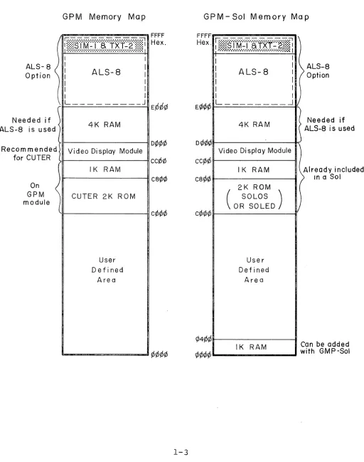
1-1 GPM and GPM-Sol Memory Maps 1-3
[image:5.612.71.542.107.754.2]SECTION 1
INTRODUCTION AND GENERAL INFOR.MA.';Q~9J~
GPM Section 1
1.1 INTRODUCTION
This manual provides all information necessary to assemble, test, and use the General Purpose Memory (GPM) Module. Before
starting to assemble the kit, scan the entire manual, and be sure that you have all the parts and components in Table 2-1, GPM
Parts List, page 2-2. All instructions are presented in the order in which you must assemble the module.
1.2 GENERAL INFORMATION
1. 2.1 Description
. The GPM is an S-lOO bus compatible memory module available in kit or assembled form for use in 8080-based computers including the Processor Technology Sol, and models by several other manufac-turers. It has a capacity of 10,240 8-bit bytes of read-only-mem-ory (ROM) for storing programs as "firmware", and 1024 bytes of read-write-memory (RAM) which is normally used as a "scratch-pad" memory. The user can store any frequently-used programs on the GPM, or use the module to house a companion product, the ALS-8 program development system, a resident monitor-assembler system, available in ROM. GPM ~ay be adapted for use with several types of ROMs and PROMs including types 92l6B, 83l6E, 34000P, and
2708. A switch-selectable automatic start-up mode is included, so that the system is "up" and ready to accept commands as soon as power is applied. All signal lines are fully buffered.
The GPM memory is available separately or as a component module in a system of five modules; "Subsystem BII, by Processor Technology. Subsystem B includes CUTS, VDM-l, 3P+S, and a choice of RAM memory boards, as well as the GPM. CUTS provides cassette tape mass storage interface; VDM-l provides a powerful video dis-play interface; 3P+S provides parallel and serial data channels for keyboard, TTY, paper tape reader or other peripherals; the R~1
memory provides working systems storage area. GPM fits into this system by providing the CUTER monitor program, and space for the ALS-8 program development system or other "firmware". Overall, Sub-system B turns the mainframe computer offered by many manufacturers into a powerful integrated computer system.
1. 2.2 GPM and GPM-Sol Versions
Two versions of the product are available; GPM-Sol, for use in the Sol Terminal Computer by Processor Technology, and GPM, for use in other S-lOO computers. The main differences between these two versions is illustrated· in Figure 1-1, GPM and GPM-Sol Memory Map, page 1-3~ This figure shows the full addressing capa-bility,
0000
to FFFF (hex.), of the 8080 Central Processing Unit used in S-lOO computers and how the subsections of the GPM and the GPM-Sol may be addressed within this range. The right-handPROCESSOR TECHNOLOGY CORPORATION
GPM Section 1
figure shows the GPM-Sol sections mapped within the Sol addressing structure, and left-hand figure shows GPM mapped within other
manufacturer's addressing structures. The main differences be-tween the two maps are:
1. The GPM version contains 2K of ROM normally addressed at locations C¢¢¢ to C8¢¢
(hexadecimal) contain CUTER (Computer User's 3ape ~ntry and Retrieval monitor program), a
version of the SOLOS monitor program used in the Processor Technology Sol. The use of this program is covered in the SOLOS/CUTER User's Manual. Since the Sol already con-tains the SOLOS program, i t is not included in the GPM-Sol version.
2. The GPM version includes lK of RAM addressed C8¢¢ to CBFF which is used by CUTER as sys-tems memory area. The GPM-Sol version does not include the RAM, since this too is
included in the Sol. However, lK of RAM may be added to the GPM-Sol, and addressed ~~~~ to ¢3FF (hex).
3. The Sol includes a video display circuit
addressed CC¢¢ to D¢¢¢. To ensure compatibility, i t is recommended that the GPM version be used in conjunction with the VDM-l Video Display
Module, which is similar to the video section of the Sol, and is also addressed CC~~ to D~¢~. 4. Both the GPM and GPM-Sol versions contain space
ALS-8 Option
\
Needed if
ALS-8 is used <
Recom mended for CUTER
On
~
GPM module
GPM Memory Map
I
I
: ALS-8
I I
1 I
I _ _ _ _ _ _ _ _ _ _ J
4K RAM
Video Display Module
IK RAM
CUTER 2K ROM
User Defined
Area
D¢rp¢
cCrD¢
ca¢¢
c¢¢¢
1-3
GPM-Sol Memory Map
FFFF
Hex . I':';·:·:·S I M-I aT ·r:::::::::·;·;·;~·;·;·;·;·;·;·;·;·;·;·"";)(f·;·;·~::~:r - •.... ;.1
;.:.:.:.: •.••••.•. ~ ... ;.~.~.~.~.;.:.:.:..:.:.:.:.:.:,:.:.:::.::~ I
I I
I I ALS-8 I I
I I
I I
I I
h
)
ALS-8 Option
L - - ______
..Jv
Dr/Jr/>¢
CqD¢
carpr/J
4K RAM
Video Di splay Module
IK RAM
(
2K ROM SOLOS)
OR SOLED
User Defined
Are a
IK RAM
)
>
j
(
/
Needed if ALS-8 is used
Already included In a Sol
[image:9.612.56.568.94.743.2]GPM
1. 2.3
PROCESSOR TECHNOLOGY CORPORATION
Section 1
an 8080 simulator, a text editor, and sup-port routines for file-handling, program
execution, and debugging. When ALS-8 is used on either GPM or GPM-Sol, 4K of RAM must be added at locations D000 to E000.
GPM Voltage Requirements, Typical
The basic GPM board requires: +7.5 to +10 V dc at 750 rna.,
Each additional 2708 draws:
Each additional 9216 draws:
+15 to +18 V dc at 50 rna., and -15 to -18 V dc at 50 rna.
+7.5 to +10 V dc, 6 rna. , +15 to +18 V dc, 50 rna. , and -15 to -18 V dc, 30 mao
+7.5 to +10 V dc, 15 mao , and +15 to +18 V dc, 50 mao
1.3 WARRANTY AND REPLACEMENT INFORMATION 1.3.1 Receiving Inspection
When your kit arrives, examine the shipping container, noting any conditions that might indicate damage to the contents during transit. Then inspect the contents. (We suggest you save the shipping materials for use in returning the Kit to Processor Technology if i t is necessary. If your GPM is damaged, please write us at once describing the condition of both the shipping container and the contents, so that we can take appropriate action.
1.3.2 Warranty Information
In brief, parts that fail because of defects in materials or workmanship are replaced at no charge for 3 months for kits,
and one year for assembled products, following the date of purchase. Also, products assembled by the buyer are warranted for a period of
3 months after the date of purchase; factory assembled units are warranted for one year after the date of purchase. Refer to Appendix I for the complete "Statement of Warranty".
1. 3.3 Replacement Parts
Order replacement parts by component nomenclature CDM8l3l IC or lN2222 diode, for example) and/or a complete description
GPM Section 1
1.3.4 Factory Service
In addition to in-warranty service, Processor Technology also provides factory repair service on out-of warranty products. Before returning the unit to Processor Technology, obtain
authorization to do so by writing us a letter describing the
problem. After you receive our authorization to return the unit, proceed as follows:
1. Write a description of the problem. 2. Securely pack the unit and the
des-cription in a shipping container. 3. Ship prepaid to Processor Technology
Corporation, 6200 Hollis Street, Emeryville, CA. 94608
Your unit will be repaired as soon as possible after receipt and returned to you prepaid. (Factory service charges will not exceed $20.00 without prior notification and your
approval).
SECTION 2
ASSEMBLY
GPM Section 2
2.1 PARTS AND COMPONENTS
Check all parts and components against the "Parts List" (Table 2-1 on Page 2-2). If you have difficulty in identifying any parts by sight, refer to the Component Identification Illustrations,
following page 2-2. 2.2 ASSEMBLY TIPS
1. Read Sections 2 and 3 before you start to assemble your GPM.
2. Assembly steps and component installations are preceded by a set of parentheses. Check off each installation and step as you complete them. This will minimize the chances of omitting a step or component.
3. When installing components, make use of the assembly aids that are incorporated on the GPM PC board and the
assembly drawing. (These aids are designed to assist you in correctly installing the components.)
4. In assembling your GPM, follow the step-by-step integrated assembly-test procedure. FOLLOW THE INSTRUCTIONS IN
THE ORDER GIVEN. The circuit reference· (R3, CIO, and U7, for example) for each component is silk screened on the PC board near the location of its installation. Both the circuit reference and value or nomenclature
(1.5k and 74LS08, for example) for each component are included on the assembly drawing near the location of its installation.
5. To simplify reading resistor values after installation, install resistors so that their color codes read from left-to-right and top-to-bottom as appropriate (board oriented as defined in Paragraph 2.5 on Page 2-6).
6. Unless specified otherwise in the instructions, install all components, especially disc capacitors, as close to the board as possible.
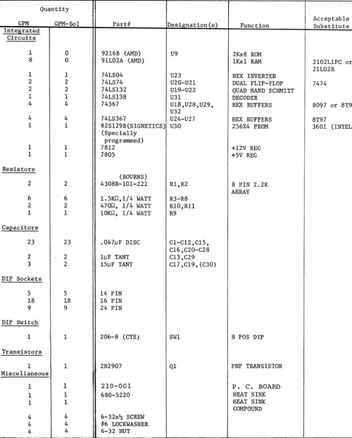
Table 2-1. GPM Parts List
Quantity
Designation(s) Acceptable
GPM GPM-So1 Pard Function Substitute
Integrated Circuits
1 0 9216B (AMD) U9 2Kx8 ROM
8 0 91L02A (AMD) 1Kx1 RAM 2102L1PC or
21L02B
1 1 74LS04 U23 HEX INVERTER
2 2 74LS74 U2O-U21 DUAL FLIP-FLOP 7474
2 2 74LS132 U19-U22 QUAD NAND SCHMITT
1 1 74LS138 U31 DECODER
4 4 74367 U18,U28,U29, HEX BUFFERS 8097 or 8T97
U32
4 4 74LS367 U24-U27 HEX BUFFERS 8T97
1 1 82S129B(SIGNETICS) U30 256X4 PROM 3601 (INTEL)
(Specially programmed)
1 1 7812 +12V REG
1 1 7805 +5V REG
Resistors
(BOURNS)
2 2 4308R-101-222 R1,R2 8 PIN 2.2K
ARRAY
6 6 1.5Im,1/4 WATT R3-R8
2 2 470n, 1/4 WATT R10,Rll
1 1 10Im, 1/4 WATT R9
CaEacitors
23 23 .04711F DISC C1-C12,C15,
C16,C20-C28
2 2 l11F TANT C13,C29
3 2 15]lF TANT C17 ,C19, (C30)
DIP Sockets
5 5 14 PIN
18 18 16 PIN
9 9 24 PIN
DIP Switch
1 1 206-8 (CTS) SW1 8 POS DIP
Transistors
1 1 2N2907 Q1 PNP TRANSISTOR
Miscellaneous
1 1 210-001 P. C. BOARD
1 1 680-5220 HEAT SINK
1 1 HEAT SINK
COMPOUND
4 4 6-32x~ SCREW
4 4 1/6 LOCKWASHER
[image:14.620.52.553.68.691.2]GPM Section 2
COMPONENT IDENTIFICATION ILLUSTRATIONS
NOTE: Pin 1 may be indicated by corner dot or cut-out
Dual Inline Package (DIP) IC (8,14,16,24 or 40 pins)
pin l~ pin 1 indicated by DIP Socket
Carbon Film Resistor 5% (gold), l~~ (silver)
DIP Switch
(+) lead
Dipped Tantalum Electrolytic Capacitor
"
f CTransistor
TO-18 Package (Metal Can)
Star Lockwasher Resistor Network
Disc Ceramic Capacitor
PROCESSOR TECHNOLOGY CORPORATION
GPM Section 2
2.3 ASSEMBLY PRECAUTIONS
2.3.1 Handling MOS Integrated Circuits
Many of the ICs used in the GPM are MOS devices. They can be damaged by static electricity discharge. Always handle MOS ICs
so that no discharge will flow through the IC. Also, avoid unnecessary handling, and wear cotton--NOT synthetic--clothing when handling
these ICs. 2.3.2
2.3.3
Soldering **IMPORTANT**
1. Use a fine tip, low-wattage iron, 25 watts maximum. 2. DO NOT use excessive amounts of solder. DO solder as
neatly and as quickly as possible.
3. Use only 60-40 rosin-core solder. NEVER use acid-core solder or externally applied fluxes.
4. To prevent solder bridges, position iron tip so that i t does not touch adjacent pins and/or traces
simultaneously.
5·. DO NOT rest tip of iron on pad or trace. To do so can cause the pad or trace to "lift" off the board and permanently damage it.
6. The GPM circuit board has plated-through holes. Solder flow through the component (front) side of the board can produce solder bridges. Check for such bridges after you install each component.
7. The GPM circuit board has an integral solder mask
(a lacquer coating) that shields selected areas on the board. This mask minimizes the chances of creating solder bridges during the assembly. DO, however, check all solder joints for possible bridges. 8. Additional pointers on soldering are provided in
Appendix 3 of this manual.
Installing and removing GPM Module.
GPM Section 2
2.3.4 Installing and Removing Integrated Circuits.
NEVER install or remove integrated circuits while power is applied to the GPM. To do so can damage the IC.
2.3.5 Use of Clip Leads
NEVER attach clip leads to the top edge of the GPM circuit board. Clip leads so attached are apt to short the +8, +16, -16 V dc, and ground buses.
2.4 REQUIRED TOOLS, EQUIPMENT AND MATERIALS
The following tools, equipment, and materials are recommended for assembling and testing the GPM Module:
1. Needle nose pliers 2. Diagonal cutters
3. Screwdriver 4. Sharp knife
5. Controlled heat fine tip soldering iron, 25 watts 6. 60-40 rosin-core solder (supplied)
7. Volt-ohm meter
2.5 ORIENTATION
The heat sink area (large foil area) will be located in the upper right hand corner of the board when the 100-pin edge connector is at the bottom. In this position the component (front) side of the board"is facing up and the solder (back) side is facing down. Also, the IC legends (Ul through U9, UIO through U18, etc.) will read from left to right. The assembly drawing in Section 5
reflects this position. Subsequent position references in the instructions assume this orientation.
2.6 ASSEMBLY-TEST
Refer to the GPM assembly drawing, Figure 5-1, in Section 5. Note that the assembly drawing shows values, e.g. 1.5K, as well as circuit references, e.g. R3.
GPM
PROCESSOR TECHNOLOGY CORPORATION
NOTE
Instructions preceded with an asterisk (*) do not apply to the GPM-Sol.
CAUTION
Section 2
THIS DEVICE USES MOS MEMORY INTEGRATED CIRCUITS WHICH CAN BE DAMAGED BY STATIC ELECTRICITY DISCHARGES. HANDLE THESE ICs SO THAT NO DISCHARGE FLOWS THROUGH THE IC. AVOID UNNECESSARY HANDLING AND WEAR COTTON RATHER THAN SYNTHETIC CLOTHING WHEN HANDLING THESE ICs. (STATIC DISCHARGE PROBLEMS ARE MUCH WORSE IN LOW HUMIDITY ENVIRONMENTS. )
2.6.1 / / Circuit Board Check
.vI)
Visually check GPM circuit board for solder bridges (shorts)between traces, broken traces, and similar defects. ( ) Check board to ensure that the +8, +16, -16, +12, +5,
-5 volt buses are not shorted to one another or to ground. Using an ohmmeter, make the following measurements (refer to GPM assembly drawing in Section 5). You should measure
j
no continuity in any of these measurements.( +8-volt Bus Test. Measure between edge connector pin 1 or 51 (left end of connector) and pin 50 or 100 (right end of . connector).
(~(
+16-volt Bus Test. Measure between edge connector pin 2 (second top, or front, pin from left end of connector) and pin 50 or 100.-16-volt Bus Test. Measure between edge connector pin 52 (second bottom, or back, pin from left end of connector) and pin 50 or 100.
,.(/) +5-vol t Bus Test. Measure between positive (+) mounting pad for C13 and edge connector pin 50 or 100.
i
(.') +12-volt Bus Test. Measure between positive (+) mounting
I ,pad for C29 and edge connector pin 50 or 100.
/
(i
GPM Section 2
( ) 8/16/(-16)/5/(-5)/12 Volt Bus Test. Measure between:
A. Edge ,Connector pins 1 or 51
and--/
~/) ,Edge connector pin 2 (.\ ) ,-Edge connector pin 52
V)
positive (+) pad for C13) Negative (- ) pad for C14
( positive ( +) pad for C29 B. Edge Connector pin 2
and--( ) Edge Connector pin 52
t/~Positive
( +) pad for C13Negative (-) pad for C14
j( Positive ( +) pad for C29 C. Edge connector pin 52
and--(
/)
/ ' Positive ( +) pad for C13
.( Negative (-) pad for C14
:<
positive ( +) pad for C29D. Positive ( +) pad for C13
and--1(/) Negative (-) pad for C14
(, ) Positive (+) pad for C29 Negq,ti ve (-) pad for C14
and--v(
Positive ( +) pad for C29E.
If you measure continuity in any of the preceding tests, recheck the measurement(s). If you still measure continuity, the board is defective. Return i t to Processor Technology for replacement. If none of the measurements show continuity, go on to the next paragraph.
PROCESSOR TECHNOLOGY CORPORATION
GPM Section 2
2.6.2
~/~ssemblY-Test
Procedure.~
Step 1. Install heat sink. Position the large, black heat sink (flat side to board) over the square foil area in the upper right corner. Orient the sink so that the two triangles of mounting holes in the board are under the two triangular cutouts in the sink. Using two 6-32 screws, lockwashers and nuts, attach heat sink to board. Insert the screws from back (solder) side of board.Step 2. Install U34 (7805). Position U34 over left hand cutout in heat sink and observe how the leads must be bent to fit the mounting pads. Note that the center lead (3) must be bent down at a point approximately 0.2 inches
further from the body than the other two leads. Bend leads so that no contact is made with the heat sink when U34
is flat against the sink and its mounting hole is aligned with the hole in the sink. Coat both the bottom surface of U34 and the heat sink area to which U34 mates with a thin film of heat sInk compound. Insert leads and fasten U34 to sink with a 6-32 screw, #6 lockwasher and nut. Insert screw from solder (back) side of board, place washer on screw and drive nut. Solder and trim leads.
NOTE
U35, the negative supply regulator, is not- supplied / with standard GPM modules. It is needed only when
i
2708 ROMs are used. (Refer to Section 3).( ) Step 3. Install U33 (7812). position U33 in the upper right hand corner of the board with the leads facing left. Observe how the leads must be bent down to fit the mounting pads and bend accordingly. U33 should lie flat against the board with its mounting hole aligned with the hole in the circuit board. Insert leads and fasten U33 to board with a 6-32 screw, #6 lockwasher and nut. Insert screw from solder (back) of board, place washer on screw and drive nut. Solder and trim leads.
GPM Section 2
( ) Step 5. Install all resistors in numerical order in the following locations. Bend leads down to fit distance between mounting holes, insert leads, pull down snug to board, bend leads outward on solder (back) side of board, solder and trim.
LOCATION VALUE (ohms) COLOR CODE
R3 R4 R5
R6
R7 R8 R9 R10 Rll
1.5k 1.5k 1.5k 1.5k 1. 5k 1.5k 10K 470 470
brown-green-red brown-green-red brown-green-red brown-green-red brown-green-red brown-green-red brown-black-orange yellow-violet-brown yellow-violet-brown Step 6. Install resistor networks Rl and R2 (2.2k ohms) in their respective locations. Position Rl and R2 so that the dot on their packages is at the bottom right. Insert leads, solder and trim.
CAUTION
RESISTOR NETWORKS ARE DELICATE. HANDLE WITH CARE. ( ) Step 7. Install the five tantalum capacitors in the
following locations. Take care to observe the proper value and orientation for each installation.
LOCATION VALUE (ufd) ORIENTATION
~) 03 1 n+n lead right
C14 (not used)
----'-1 C17 15 n+n lead bottom right
C18 (not used)
~7f C19 15 n+n lead right
r}- C29 1 n+n lead right
~J~
..
t,
C30 15 n+n lead down
-~*
C30 is not marked on the board. the right of IC socket U20.It is the unmarked capacitor to.
NOTE
C14 and C18 are not supplied with standard GPM modules. They are needed only when ROMs that
require -5 V dc are used. (Refer to Section 3.3.2, steps 2 and 3.)
PROCESSOR TECHNOLOGY CORPORATION
GPM Section 2
( ) Step 8. Install all disc capacitors in numerical order in the following locations. Insert leads, pull down snug to board, bend leads outward on solder (back) side of board, solder and trim.
( ) ( )
( )
( ) ( ) ( ) ( ) ( )
( ) ( ) ( )
NOTE
Disc capacitor leads are usually coated with wax during the manufacturing process. After inserting leads through mounting holes, remove capacitor and clear the holes of any wax. Re-insert and install.
LOCATION VALUE (ufd) TYPE
CI .047 Disc Ceramic
C2 .047 Disc Ceramic
C3 .047 Disc Ceramic
C4 .047 Disc Ceramic
CS .047 Disc Ceramic
C6 .047 Disc Ceramic
C7 .047 Disc Ceramic
C8 .047 Disc Ceramic
C9 .047 Disc Ceramic
CIO .047 Disc Ceramic
CII .047 Disc Ceramic
_LJ_CI_2_ .047 Disc Ceramic
, ( ) CIS. .047 Disc Ceramic
_.LJ ____
.cL6----. .047 Disc Ceramic( ) ( ) ( )
( )
( )
( )
( )
( ) ( )
C20 .047 Disc Ceramic
C21 .047 Disc Ceramic
C22 .047 Disc Ceramic
C23 .047 Disc Ceramic
C24 .047 Disc Ceramic
C2S .047 Disc Ceramic
C26 .047 Disc Ceramic
C27 .047 Disc Ceramic
C28 .047 Disc Ceramic
GPM Section 2
INSTALLATION TIP
Insert socket pins into mounting pads of
appropriate location. On back (solder) side of board, bend pins at opposite corners of socket (e.g. pins 1 and 9 on a 16-pin socket) outward
until they are at a 45° angle to the board surface. This secures the socket until i t is soldered.
Repeat this procedure with each socket until all are secured to the board. Solder the unbent pins on all sockets. Then straighten the bent pins to their original position and solder.
NOTE
If you intend to use eight lK ROMs instead of four 2K ROMs, 24-pin sockets should be installed in these four locations.
LOCATION SOCKET TYPE
I"'~;'
/ !
Ul through "Q9 24 pin 16 pin 14 pin 16 pin UIO through U18
U19 through U23 U24 through U32
( ) Step 10. Check regulator operation. This check is made to prevent potential damage to the ICs from incorrect voltages.
( ) Using an ohmmeter, make the following measurements: SUPPLY
+5 V de +12 V de
l-fEASUREMENT POINTS
Positive (+) and negative (-) leads of C13 Positive (+) and negative (-) leads of C29 You should measure some resistance in both measurements.
Zero resistance indicates a short. If required, find and correct the problem before proceeding. Especially check for solder bridges.
( ) Install GPM in computer. (The use of a Processor Technology EXB Extender Board is recommended.)
GPM
PROCESSOR TECHNOLOGY CORPORATION
Section 2
CAUTION
NEVER INSTALL OR REMOVE GPM WITH POWER ON.
( ) Turn power on and make the following voltage measurements: MEASUREMENT POINTS
Across C13 Across C29
VOLTAGE (±5 % )
+5 V dc +12 V dc
If either voltage is incorrect, determine and correct the cause before proceeding. If voltages are correct, turn power off, remove GPM from computer and go on to step 11. ( ) step 11. Install the following ICs in the indicated
locations. Pay careful attention to the proper orientation.
* ( )
* ( )
(~
.~ ~
«(---)
N
l(~-+
f.i.r
( )
( )
(...4--NOTE
Pin 1 is positioned in the lower right corner of each IC location, and is indicated by a dot on the assembly drawing.
IC NO. U9#
UIO through 17# U18
U19
U20 & 21
U22 U23
U24 through
21')
U28 & 29
U30 U31 U32
TYPE
9216# (CUTER ROM)
91L02A, 2102LIPC or 21L02B# 74367, 8097 or 8T97
74LS132 or 74132 74LS74 or 7474 74LS132 or 74132 74LS04 or 7404 74LS367 or 8T97
74367, 8097, or 8T97 82S129 or 3601
74LS138 or 74158 74367, 8097, or 8T97
*
#MOS devices. Refer to CAUTION on Page 2-8.GPM Section 2
As presently assembled, the GPM is configured to operate with 92l6B ROMs in locations U2, U4, U6, U8, and U9. Other 2K ROMs
(34000 and 83l6E) can also be used in these locations by recon-figuring the board via trace cutting and jumper options. In a
similar manner the GPM can be reconfigured to use lK ROMs (e.g. 2708) in locations Ul through U8. Instructions for making the required changes are given in Section 3.
( ) Step 12. Install transistor 2N2907 according to the following instructions. Place the middle lead of the transistor in the hole labeled B (right below and to the left of R4 on the component side). The small metal tab should point to the left; then the other two leads will fit into the appropriate holes. Install the transistor as close to the board as possible. Turn the board over, solder ·the leads and trim.
2.6.3 ALS-8, and ALS-8 with SIM-l and TXT-2 Options
If you have purchased either the ALS-8 option alone, or the ALS-8 plus SIM-l and TXT-2 option, and your GPM or GPM-Sol board is functioning correctly, you may proceed to install these ROMs
according to the instructions enclosed with them. 2.6.4 Operation in Computers without Sense Switches
At start-up, after examining location C~~~, the CUTER program inputs the sense switch data from port FF (hexadecimal) to determine the input and output pseudoports to be used during command mode. If the system has no sense switches, data from port .FF will be input as
FF which indicates that at locations C8~~ and C8~2 the program will find the addresses of user-defined input and output routines. By putting the addresses of pre-written CUTER routines in these two locations, the desired command mode input and output routines are selected without sense switches. By entering the data in the table below before examining C~~~ and running, the desired input and out-put routines may be chosen. Entering these addresses is known as patching.
1. INPUT PATCH:
at C8~~ patch in:
2. OUTPUT PATCH:
35C~ for keyboard input 3EC~ for serial input 5~C~ for parallel input
at C8~2 patch in 77C~ for video display output" 46C~ for serial output
SECTION 3
GPM OPTIONS
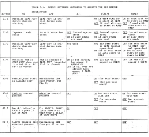
GPM Section 3
3.1 GPM OPTIONS
The eight-position DIP switch (SW1) located in the upper right corner of the PC board is used to configure the GPM for the various operating options. These include: the automatic start-up option; wait-state generation; and the ability to place portions of memory at different addresses.
Jumper arrangements are provided to permit accomodation of various types of ROM chips.
SWITCH
51-1
51-2
51-3
51-4
I
51-5TABLE 3-1. SWITCH SETTINGS NECESSARY TO OPERATE THE GPM MODULE DESCRIPTION
ON
Disables E~~~-FFFF
during phantom start-up
Imposes 1 wait state
Disables C~~~-C7FF
during phantom start-up
OFF
E~~~-FFFF is
ena-',bled during auto :start
Sol ON
No wait state im-" OFF (normal
opera-posed tion)
" .--~ ..
C~~~-C7FF is
ena-bled during auto start
ON if slow PROMs are used Not used
ALTAIR IMSAI ON if used with au- ON if used with au
to start at C~~~ to start at C~~
OFF if used with au- OFF if used with
- to start at E~~~ auto start at
OFF (normal opera-tion)
ON if slow PROMs are used
E~~~
OFF, (normal opera-- tion)
ON if slow PROMs are used. OFF for auto start OFF for auto start
to C~~~ (normal to C~~~
(nor-operation) mal operation) ON for no auto start ON for no auto
or auto start to start or auto
E~~~ start to E~~~
Disables RAM at RAM is enabled @ ON if Sol already OFF (IK RAM will OFF, (IK RAM will -'appear @ C8~~) ~~~~-~3FF when usee ~~~~-~3FF (provided has memory @ appear at C8~~)
in a Sol '(i.e. i f 51-7 is closed) ~~~~-~3FF
51-7 is' closed) OFF if Sol does not
Permits ,auto start Disconnects GPM in ALTAIRs only from PRESET, Bus
Pin 75
,
OFF
already have memory @ ~~~~ ~3FF
ON (for auto start) OFF (for non-auto
start)
OFF
51-,6 Enables on-card \ phalltonl
\Disables on-card iphantom
OFF ON for auto start with GPM
ON for auto start with GPM
51-7
51-8
For Sol (disables PROM 9 & puts lK RAM at ~~~~
,For ALTAIR, IMSAI, ON
(puts PROM 9 at ' . -\ CfJJ'~-C7FF & lK RAM:
,at,C8~~-CBFF) "
'Allows control from Disconnects GPM
external phantom \ from pin 67 on bus OFF
3-1
OFF for non-auto start
OFF
OFF
OFF for non-auto start
[image:27.612.85.564.277.717.2]PROCESSOR TECHNOLOGY CORPORATION
GPM Section 3
3.2 SWITCH OPTIONS
Table 3-1 "Switch Settings Necessary to Operate the GPM Module" summarizes the function of the different switchs in each of the three main types of computers: the Sol, the ALTAIR 8800, and the IMSAI 8080, in which the GPM is expected to be used. In each case, the first setting shown is the one that would
normal-ly be used and the second setting is the exception (i.e. Sl-2 is normally OFF but should be switched to ON if slow memory chips are used) •
If the GPM is to be used in any other computer, the switch functions should be studied and set according to the requirements of that computer.
3.3 READ ONLY MEMORY OPTIONS
When assembled according to the instructions in Section 2, your GPM is configured for use with 9216B (2Kx8) ROMs in locations U2, U4, U6, U8, and U9 and no memory chips in locations Ul, U3, US, and U7. By cutting specific traces and installing specific jumpers, you can configure your board to:
1. Replace any 9216B (2Kx8) ROM (U2, U4, U6, U8, and U9) with an 8316E or a 34000P ROM.
2. Replace any 9216B (2Kx8) ROM in locations U2, U4, U6, and U8 with two 2708 (lKx8) PROMs (two 2708s in Ul and U2 to replace the 9216B in U2, two 2708s in U3 and U4 to replace the 9216B in U4, two 2708s in US and U6 to replace the 9216B in U6, or two 2708s in U7 and U8 to replace the 9216B in U8). In order to use 2708 PROMs, you must also add the -5 V dc regulator circuit.
3.3.1 Replacing 9216Bs W~th 83l6Es or 34000Ps
GPM Section 3
Table 3-2. Replacing 92l6B (2Kx8) ROMs With 83l6E Or 34000P (2Kx8) ROMs
CHIP LOCATION
U2
U4
U6
U8
U9
CUT TRACE
M-P (component side) jj-kk (solder side) Q-S (solder side) gg-hh (solder side) T-W (solder side) ee-ff (solder side)
x-z
(solder side) cc-dd (solder side) J-L (component side) aa-bb (solder side)INSTALL JUMPER BETWEEN* M and GND kk and P Q and GND hh and S T and GND ff and W X and GND dd and Z J and GND bb and L *Install all jumpers on component side of board
using #24 bare wire.
Your GPM is now configured to operate with 83l6E or 34000P (2Kx8) ROMs. Return to Section II to complete assembly of your GPM module.
3.3.2 Replacing 92l6Bs With Two 2708 PROMs
If 2708 PROMs are used on the GPM module, you must install a -5 V dc regulator circuit (U35, C14, and C18). You need the
fol-lowing components and hardware. This equipment can usually be pur-chased at any local electronics store.
1 7905 regulator (U35)
1 1 ufd tantalum dipped capacitor (C14) 1 15 ufd tantalum dipped capacitor (C18) 1 6-32 x ~ screw, Nylon
1 #6 lockwasher
1 6-32 hex nut 1 Insulator, mica 1 Heat sink compound
To add this circuit, proceed as follows: (See assembly drawing in Section 5, Page 5-1.1
[image:29.612.130.520.168.436.2]GPM
PROCESSOR TECHNOLOGY CORPORATION
Section 3
( ) Step 1. Install U35 (7905). Position U35 over right hand cutout in heat sink and determine how the leads must be bent to fit the mounting holes. Note that the center lead (3) must be bent down at a point approxi-mately 0.2 inches further from the body than the other two leads. Bend leads so that no contact is made with the sink when U35 is flat against the sink and its mounting hole is aligned with the hole in the sink. Coat both sides of the mica insulator and the mating surfaces on the sink and the bottom of U35 with a thin film of heat sink compound. Insert Nylon 6-32 x ~ screw from back (solder) side of board, place insulator over screw on front (component) side, lower U35 over screw and insert leads, place #6 lockwasher on screw and drive hex nut. Solder and trim leads.
( ) Step 2. Install C14 (1 ufd tantalum dipped capacitor) in its location below the heat sink, position C14 with its positive (+) lead to the left, insert leads, solder and trim.
( ) Step 3. Install C18 (15 ufd tantalum dipped capacitor) in its location in lower left corner of board (below U9) . Position C18 with its positive (+) lead at the top, in-sert leads, solder and trim.
( ) Step 4. Check regulator operation. This check is made to prevent potential damage to the ICs from an incorrect voltage. Using an ohmmeter, measure between positive
(+) and negative (-) leads of C14. You should measure some resistance. Zero resistance indicates a short. If required, find and correct the problem before proceeding. Especially check for solder bridges.
( ) Install the GPM in computer. (The use of a Processor Technology EXB Extender Board is recommended.)
CAUTION
NEVER INSTALL OR REMOVE GPM WITH POWER ON.
GPM Section 3
A summary of traces to be cut and jumpers to be added to replace a 92l6B (2Kx8) ROM (U2, U4, U6, and U8) with two 2708
(lKx8) PROMs are given in Table 3-3. Figure 3-1 shows the loca-tions of the traces to be cut and the jumpers to be installed.
These locations are also printed on the circuit board legend. Table 3-3. Replacing 92l6B (2Kx8) ROMs With 2708
(lKx8) ROMs
CHIP LOCATION Ul, U2
U3, U4
U5, U6
U7, U8
CUT TRACE
M-P (component side) G-H (component side) Q-S (solder side) E-F (component side) T-W (solder side) C-D (component side)
x-z
(solder side) A-B (component side)INSTALL JUMPER BETWEEN* M and N
Q and R
T and V
X and Y
*Install all jumpers on component side of board using #24 bare wire.
Your GPM is now configured to operate with 2708(lKx8) EPROMs. Return to Section 2 to complete assembly of your GPM module.
[image:31.612.110.547.129.442.2]Component (front) Sid e
UI
U2
U3
U4
U5
U6
U7
us
U9
So Ide r (b a c k) Si de
U9
us
U7
U6
U5
U4
U3
U2
UI
0
I
r
jO
I~
I
j:
t
t
~
t ( t
~
w
ITj
1-'-I.Q C
Ii
CD
w
I
I-'
.
v t'i
!iii! 0
!iii! 0
0 PI
0
rt
1-'-0
=' rn
HI
0
Ii
8
Ii
PI
0
CiI Iii G - .. "'111111
I~IJ~
ll'IIIJ
CD\)J1--
()c
rt rn
PI
-;:s Po
Col
THEORY OF OPERATION
PROCESSOR TECHNOLOGY CORPORATION
GPM Section 4
4.1 OVERVIEW
The GPM consists of up to 10K of ROM, lK of RAM, an address decoder, a phantom (automatic) start-up circuit, a wait state cir-cuit, and on-board voltage regulator circuits. While reading the circuit description, pullout the schematic in Section V, Figure 5-2. Also refer to the GPM and GPM-Sol Memory Map in Section 1, Figure 1-1.
4.2 CIRCUIT DESCRIPTION
4.2.1 Address Decoding
Address lines AO through A9 are buffered from the bus through U25 and U26 to the 10 address pins on each RAM chip (UIO through U17) and ROM/PROM chip (Ul through U9). AIO, buffered through U24, is ap-plied to the AIO input to U2, U4, U6, and U8. AIO also appears on
pin 21 of U9, and AO input to U30 and the A input to U31. In addition, AIO provides the enables for ROM chip select drivers U18 and PROM chip enable drivers U29.
The address decoding is done with an 82S129 256x4 PROM (U30), and a small amount of support circuitry. The four outputs of the 82S129 are CARD SELECT, ROM C, ROM EF, and
RAM.
Any time the 82S129 gets an address that one of the memories on the card should respond to, both CARD SELECT and the appropriate memory line (ROM C,ROM EF,
orRAM) are activated. Whenever CARD SELECT is activated (active low),
the buffers from both the wait state circuitry (which outputs to the PRDY line and will be discussed below) and from pin 11 of U22 are activated. Since the inputs to this NAND gate are PDBIN and SMEMR, output 11 will go low whenever the processor is requesting data from memory. Thus, when CARD SELECT is low pin 13 of U32 will go low when-ever the processor is requesting data. This signal goes to both U20
(the phantom start-up circuitry which will be discussed later) and to enable the data bus drivers, U28 and U29. So, whenever data is re-quested from one of the memories on the GPM, the appropriate memory line (ROM C, ROM EF, or RAM) is activated as well as CARD SELECT
which in turn activates both the wait state output driver and the data bus drivers.
GPM Section 4
Table 4-1. Memory Allocation Table
Sol (Sl-7 is ON) Non-Sol
Memory
NORMAL NORMAL
Line PHANTOM PHANTOM
OPERATION OPERATION
\
ROM C None None ~~~~-~3FF C~~~-C7FF
(if Sl':"3 is open)
ROIVI EF None E~~~-EFFF ~~~~-~3FF EIdIdId-FFFF
(if Sl-l is open)
RAM None ~Id~~-~3FF None C8~Id-CBFF
4.2.2 Memory Allocation
The memory block
EIdIdId
to FFFF consists of either four 2K ROMs (U2, U4, U6, and U8) or eight lK PROMs (Ul through U8). Memory allo-cations for this block are as follows:ROM CONFIGURATION
SOCKET 4-2K CHIPS 8-1K CHIPS
Ul F8Id~
-
FBFFU2
F8IdId -
FFFF FC~Id - FFFFU3 FId~~
-
F3FFU4 F~~~ - F7FF F4Id~
-
F7FFUS
F80Id -
EBFFU6 E8Id~
-
EFFF EC~Id - EFFFU7 E~Id~
-
E3FFU8 E~~~ - E7FF E4Id~
-
E7FF.t<lemory block C~~Id
-
C7FF is assigned to U9, a 2K ROM .The lK of RAM (U10 through U17) can be addressed at either
C8IdId -
CBFF when the GPM is used with non-Sol computers at ~IdId~-~3FF when i t is used with the Sol. [image:35.612.40.554.155.369.2]
PROCESSER TECHNOLOGY CORPORATION
GPM Section 4
4.2.3 Read Operation
In a GPM read operation, data is read from either ROM/PROM or RAM, as requested, to the Data In Bus (DI~-7) via buffers U28 and U29. The Data Out (DO) outputs of the
RAM
and ROM/PROM chips are tri-stated types that float in a high impedance state when they are not selected. They are therefore connected in parallel. As a result, only the bits in the addressed memory can be gated to DIO-7.Assuming the processor requests data from the GPM (PDBIN and SMEMR are both high on Bus Pins 78 and 47 respectively and i t is ap-propriately addressed), CARD SELECT and the applicable memory line are activated.
CARD SELECT (active low) enables the PRDY (Bus pin 72) line driver, U32-ll, and enables U32-l3. With Sl-2 open, PRDY will be high and the processor will be in the run state. One wait state is imposed if Sl-2 is closed. (Refer to Paragraph 4.2.6) Since PDBIN and SMEMR are low when the GPM is accessed, the low on pin 13 of U32 enables the DI Bus drivers U28 and U29.
Should the RAM be addressed, RAM is low to enable UIO through U17 to present data to U18 and U29, the DI Bus drivers. Note that RAM also enables U24-9 which gates the inverted MEM WR (Bus pin 68) to the WE inputs of each RAM chip. MEM WR is low for a read opera-tion, so the WE input is high. RAM can also be applied to pin 15 of U30 through Sl-3. This disables the RAM at ~~~.~ - ~3FF.
If U9 is addressed, ROM C will be active
(hig~'),
and provi-ding PHANTOM is not low on U22-9 through Sl-3, U22-8 is low to enable U9 to present data to the DI Bus drivers.With ROM EF active (low), U3l decodes address lines AlO, All, and A12 to determine which of Ul through U8 is to be accessed. The enables for U2, U4, U6, and U8 are gated when AlO is high by U18, and the enables for Ul, U3, U5, and U7 are gated when AlO is low by U29. Switch Sl-l determines whether or not E~~~ - EFFF is disabled
(Sl-l closed) during automatic start-up.
4.2.4 Write Operation
GPM Section 4 The main difference between a read and a write operation is that in a write operation MEM WR is high instead of SMEMR and only the RAM will be active. In this case the low on pin 6 of U19 is gated to the WE input of each RAM so that the data on the DO Bus can be written into UIO through U17.
4.2.5 Phantom (Automatic) Start-Up
The phantom start-up circuitry (see GPM Schematic, Section 5, Figure 5-2) consists of flip-flop U20 and one-half of U21. When the power is turned on, POC (Bus pin 99) resets the R-S flip-flop which consists of two (2) gates from U22 pulling pin 3 low. This, in turn, resets the phantom flip-flops. As C30 charges up, i t turns Ql off. With Ql off, Rll pulls pin 1 low, which sets the R-S flip-flop
(U22-3) high. Pin 5 of U21, which has been reset to zero (0), pulls pin 15 of the 82S129 ROM (U30) low from pin 11 of U18 (provided Sl-6 is closed). Thus, the memories on the board will respond as indi-cated under PHANTOM start-up in Table 3-1.
If PRESET is pulled low (either through Sl-5 in an ALTAIR 8800 or from the front panel of an IMSAI 8080), the processor begins executing code at ~~~~. The first four bytes in ROM C or ROM EF will be typically one byte NOOP (~~) and a three byte JMP (C3
xx
XX). As the processor reads these four bytes, U20 counts the memory access pulses from pin 13 of U32. Pin 5 of U21 goes high on the fourth access, the GPM goes into normal operation, and the processor jumps to address XX XX to begin executing code.4.2.6 Wait State Circuit
The Q output of wait state flip-flop, U21-9, is reset low by PSYNC (Bus pin 76) at the start of each machine cycle. An inverted 2 from pin 3 of U19 clocks U21-9 back to a high at the end of each machine cycle. Consequently U21-9 generates a wait state that is one machine cycle in duration.
If Sl-2 is closed, this wait state is placed on the PRDY line (Bus pin 72) via U32-11 each time the GPM is accessed. This causes the processor to enter the wait condition and allows the GPM two cycles, rather than one, to respond.
4.2.7 Regulators
U33 and U34, series voltage regulators, supply on-card regu-lation to maintain constant +12 V and +5 V dc outputs respectively.
(If installed, U35 provides on-card regulation to maintain a constant -5 V dc output.) Input capacitor C17 provides additional filtering of the +8 V dc input, as does C19 for the +18 V dc input. The
out-put bypass capacitors C13 and C29 improve transient response. (CIB and C14 in the -5 V dc regulator, if installed, serve the same functions as their counterparts in the +12 and +5 V dc supplies.)
SECTION 5
-! » 1'.:1 """ o o o -" COMPONENT OF' J,1~
~O
"" C
=!
+9 +
+16
-m
w
-J mJ
X R O Y - - - 0 5 1 3
-
0----VI1 RTC
-VI2 5TSTB
VI3 0lG1
VI4 FROY -VI
VUi - - - -~----
VI?
XROY2
M W R T
-UNPROC - - PROC - - 2 0 - 7 0
55 RUN
-2 CLK P H O L O
-1 CLK -PRESET - 2 5 - 7 5 PHLOA P S Y N C P W A I T
-PINTE - - - POBIN
--~--AS AO
~ ~ f'!:. .,
A::3 "" A2
A15 AS
A12 A7
A9 AS
DO 1 A1:3 0 0 0 A14
A10 A11
0 0 4 0 0 2 0 0 5 DO :3
DO S DO 7 - - - 4 0 - 9 0 01 2 tU 4
01 :3 0 1 5 0 1 7 01 S SMI· 01 1 SOUT 01 SINP SINTA
5MER SWO
5 H L T A S S T A C K
-CLOCK POC -ONO G N O - 50-100
~
_.
~tr
~l~
~Jt-cI
~
·I:S:Ii~ CD (Jl
t
III
mJr-m
...
t!o
-Z
=!
I
~
~~
-... "'U1
Pt7~IN
~MI1MII: MiMWII: ... INP
r'Il)INTOM
C-
f'ff' fi '3 f'.'. ((.,. ~I~.~)~~·.' C os: f",\~. f' '.
i
_1" :,~\",~~ ~ $$ :,~ •.. )1 , .. I .... 1 -10
Ie
sz. -17V
All a7>---~~~~ ~:~,,~---_+---r_---.
>-;- ... 'f1p.;,---,
I UlJl '15>:>J
AI" ~
A!? ~>,-tl+---,
t.::..:/uzs~
A4~1-'-""""uzs~
""13. ~+5V
r---+---~~---+_----~---_+---._---~---_+--,---~----._---_+----~~---+----~
1':1 f(z. !':'z. p:z. !':'z. 1":2- I': I
11:2-z. e 3 7 z. 5 4 A
-U~
l
~!SOO'::'4-0G----.
____~_/~
_ _ ,9--+__+---* _ b , ___~
___I_---~-;-V-
..+-:--_+---8-7-7-'7-U-~-~--.-~--_+---.
_ _ _ _~.:_.
_ _;--+---i-u-~-~-/_.,,-
"~..__.+---8"-'-7~-':--U~':
.,.tz.v~~ ~~
HkKr~
E phh~5_'
__~~---C--~O~----~---f-f-r~·~-~-~--_~---n----B---~---~t~~~J~dG
'-'''''----'' .. f--... - .
.---;---rr--~---+~---+----.----1~--~~~r+~---r_~~.~---r__- ·r-~++~---~_rr+~----r-'--rr--~·+1~---~--r~+-~---+_-- ----j-~_j~---··-···--__j-_+_++_._--_+---H_+~_+_ ..
.---;---++--++;-~---r__++;~~--;_--_++___j_+r+~---_+--+;_r~----~.--,,--_+_++;_~---+_--j_rr+~--_+----++--_+r+~---.----.+_~~~~--~----_r+1~~
Y+-H-+-H--j-+ ... - - -... ~++-++H·-H-1-·,,,----,, .. · .-- ... ~-·----~-++_H-I-H~~----~~_I_+-+_++1_+~---~-HH_I_H-H~---~
L.t:j~+I:t=t+~:;:::==~~+tI+ttt:1~==~:i:ti+ttti+h:--'---l~++--I~++-I-4""
.
r---+-·+-+-+-H-H-+,· ~ ... ---.__-++-Jf-+++++
.--.-'-t--I-++t-++-H-~.---...
+1_t_if_HI_t_H_.__----_+_+_+_H_l_+_H_H_----CHKQD, aLIAIID.
[image:40.1224.315.1211.23.769.2]1 Statement .of Warranty
2 8080 Operating Codes
3 Standard Color Code
4 Loading DIP Devices,
Soldering Tips and Installing Augat Pins
GPM
PROCESSOR TECHNOLOGY CORPORATION
Appendix 1
PROCESSOR TECHNOLOGY CORPORATION, in recognition of its responsibility to provide quality components and adequate instruction for their proper assembly, warrants its products as follows:
All components sold by Processor Technology Corporation are purchased
through normal factory distribution and any part which fails because of defects in workmanship or material will be replaced at no charge for a period of 3 months for kits, and one year for assembled modules, following the date of purchase.
The defective part must be returned postpaid to Processor Technology Corporation
within the warranty period.
Any malfunctioning module, purchased as a kit directly from Processor
Technology and returned to the factory within the three-month warranty period,
which in the judgement of PTC has been assembled with care and not subjected
to electrical or mechanical abuse, will be restored to proper operating condition and returned, regardless of cause of malfunction, without charge. Kits purchased
from authorized PTC dealers should be returned to the selling dealer for the
same warranty service.
Any modules purchased as a kit and returned to PTC, which in the
judgement of PTC are not covered by the above conditions, will be repaired
and returned at a cost commensurate with the work required. In any case, this charge will not exceed $20.00 without prior notification and approval of the owner.
Any modules, purchased as assembled units are guaranteed to meet specifications in effect at the time of manufacture for a period of at least one year following purchase. These modules are additionally guaranteed against defects in materials or workmanship for the same one year period. All warranted
factory assembled units returned to PTCO postpaid will be repaired and returned
without charge.
C3 JMP C2 JNZ CA JZ 02 .JNC
OA JC E2 JPO EA JPE F2 JP FA JM
E9 PCHL
MOVE IMMEDIATE
Adr
06 MVI B. OE MVI C. 16 MVI O. 1E MVI E. 26 MVI H. 2E MVI L. 36 MVI M. 3E MVI A.
INCREMENT**
04 INR B
OC INR C
14 INR 0
lC INR E
?4 INR H
2C INR L
34 INR M
3C INR A
03 INX B
13 INX 0
23 INX H
33 INX SP
CD CALL
C4 CNZ
CC CZ
04 CNC
DC CC Adr
E4 CPO
EC CPE
F4 CP
FC CM
Acc
IMMEDIATE*
C6 ADI CE ACI 06 SUI DE SBI
08 E6 ANI 08
EE XRI F6 ORI FE CPI
DECREMENT**
05 OCR B
00 OCR C
15 OCR 0
10 OCR E
25 DCR H
20 OCR L
35 OCR M
3D OCR A
OB OCX B
1B OCX 0
2B OCX H
3B OCX SP
C9 RET CO RNZ C8 RZ DO RNC
08 RC
EO RPO
E8 RPE FO RP
F8 RM
LOAD IMMEDIATE
C7 RST 0
CF RST 1
07 RST 2
OF RST 3
E7 RST 4
EF RST 5
F7 RST 6
FF RST 7
STACK OPS 01 11 21 31 LXI LXI LXI LXI
S'j
C5~: D16~;
SP, F5
PUSH B PUSH 0 PUSH H PUSH PSW
DOUBLE ADDT
09 DAD B
19 DAD 0
29 DAD H
39 DAD SP
LOAD/STORE
OA LDAX B 1A LDAX 0 2A LHLD Adr 3A LOA Adr
02 STAX B 12 STAX 0 22 SHLD Adr 32 STA Adr
C1 POP B
01 POP 0
El POP H
F1 POP PSW'
E3 XTHL
F9 SPHL
SPECIALS
EB XCHG
27 OAA'
2F CMA
37 STCt
3F CMC+
INPUT/OUTPUT
03 OUT 08
DB IN 08
07 RLC
OF RRC
17 RAL IF RAR
CONTROL
00 NOP
76 HLT F3 01 FB EI
MOVE
40 MOV
41 MOV
42 MOV
43 MOV
44 MOV
45 MOV
46 MOV
47 MOV
48 MOV
49 MOV
4A MOV
4B MOV
4C MOV
40 MOV
4E MOV
4F MOV
50 MOV
51 MOV
52 MOV
53 MCV
54 MOV
55 MOV
56 MOV
57 MOV
B,B B,C B,D B,E B,H B,L B,M B,A C,B C.C C,D C.E C.H C,L C,M C,A D,B D.C D,D D,E D,H D,L D,M D,A
58 MOV E,B 59 MOV E,C 5A MOV E,D 5B MOV E,E 5C MOV E,H 5D MOV E,L 5E MOV E,M 5F MOV E,A
60 MOV H,B 61 MOV H,C 62 MOV H,D 63 MOV H,E 64 MOV H,H 65 MOV H,L
66 MOV H,M
67 MOV H,A
68 MOV L,B 69 MOV L,C 6A MOV L,O 6B MOV L,E 6C MOV L,H 6D MOV L,L 6E MOV L,M 6F MOV L,A
70 MOV M,B 71 MOV M,C
72 MOV M,D
73 MOV M,E 74 MOV M,H 75 MOV M,L
77 MOV M,A
78 MOV A,B 79 MOV A.C 7A MOV A,O 7B MOV A,E 7C MOV A,H 70 MOV A,L 7E MOV A,M 7F MOV A,A
08 constant, or loglcatarlthmetic expression that evaluates to an 8 bit data quantity.
016 ~ constant, or 10gicaVarithmetic expression that evaluates to a 16 bit data quantity.
all Flags (C.Z,S.P) affected t = only CARRY affected
APPENDIX II
\ \
80 ADD B
81 ADD C
82 ADD D
83 ADD E
84 ADD H
85 ADD L
86 ADD M
87 ADD A
88 ADC B
89 ADC C
8A ADC D
8B ADC E
8C ADC H
80 ADC L
8E ADC M
8F ADC A
90 SUB B
91 SUB C
92 SUB D
93 SUB E
94 SUB H
95 SUB L
96 SUB M
97 SUB A
98 SBB B
99 SBB C
9A SBB 0
9B SBB E
9C SBB H
9D SBB L
9E SBB M
9F SBB A
AO ANA B
Al ANA C
A2 ANA D
A3 ANA E
A4 ANA H
A5 ANA L
A6 ANA M
A7 ANA A
Adr = 16 bit address
A8 XRA B
A9 XRA C
AA XRA D
AB XRA E
AC XRA H
AD XRA L
AE XRA M
AF XRA A
BO ORA B
Bl ORA C
B2 ORA 0
B3 ORA E
B4 ORA H
B5 ORA L
B6 ORA M
B7 ORA A
B8 CMP B
B9 CMP C
BA CMP 0
BB CMP E
BC CMP H
BD CMP L
BE CMP M
BF CMP A
PSEUDO INSTRUCTION
ORG Adr END
EOU D16
OS D16
DB D8 II
DW 016 I I
•• = all Flags except CARRY affected; (exception: INX & DCX affect no Flags)
OBDH
l
H lAH r ex105D
l .
105 r DeCimal720 } 720 Octal
11011B} . ool10B BInary
'TEST' } 'A' 'B' ASCII
OPERATORS
+
-STANDARD SETS
A SET 7
B SE. a
C SET 1
D SET 2
E SET 3
H SET 4
L SET 5
M SET 6
SP SET 6
PSWSET 6
PROCESSOR TECHNOLOGY CORPORATION
GPM Appendix 3
The electrical value of many types of resistors and capacitors is printed on the component. Other types, however, are identified by color coding which gives all the information needed to correctly
identify the component. In most cases color coding conforms with the EIA (Electronic Industries Association) Standard Color Code. In other cases a manufacturer will adapt the standard to fit his particular requirement. Both the Standard Color Code and a code used to identi-fy tantalum dipped capacitors are provided below.
STANDARD COLOR CODE FOR RESISTORS AND CAPACITORS
COLOR FIGURE FIGURE 1st 2nd MULTIPLIER TOLERANCE ('Yo)
Black 0 0 1
Brown 1 1 10
Red 2 2 100
Orange 3 3 1,000
Yellow 4 4 10,000
Green 5 5 100,000
Blue 6 6 1,000,000
Violet 7 7 10,000,000
Gray 8 8 100,000,000
White 9 9 1,000,000,000
Gold
-
-
0.1 5Silver
-
-
0.01 10None
-
-
---
20*Applies only to capacitors.
RATED CAPACITANCE
VOLTAGE COLOR IN PICOFARADS
VDC 25°C 1st 2nd Multiplier
Fiqure Fiqure (uuF)
3-4 Black 0 0 1
3-6 Brown 1 1 10
3 .... 10 Red 2 2 100
3-15 Orange 3 3 1,000
3-20 Yellow 4 4 10,000
3-25 Green 5 5 100,000
3-35 Blue 6 6 1,000,000
3-50 Violet 7 7 10,000,000
--
Gray 8 8---3 White 9 9
---VOLTAGE
RATING* Tolerance
--100 200 300 400 500 600 700 800 900 1000 2000 500
MUltir)
-i~~~~
r
i'"
1st and 2nd Significant
Figures
[
Polarity &
Voltage
1st Figure
GPM Appendix 4 LOADING DIP (DUAL IN-LINE PACKAGE) DEVICES
(1) Sockets. DIP sockets are marked to indicate the correct orientation for the IC which will be inserted. This mark may be a notch at the end of the socket, or a filled-in corner on the inside of the socket as shown in the Comp-onent Ientification Illustrations in Section II.
Orient the socket so that pin 1 lines up with the indication for pin 1 printed on the printed circuit board legend, which may be a white dot. Insert the socket into the board, and while pressing the socket into place to ensure that i t is
fully seated, bend two diagonally opposite pins to retain the socket in its fully seated position while soldering. (2) ICs. Many DIP devices have their leads spread so that they
may not be inserted directly into their sockets. They must be "walked in" using the following procedure.
Orient pin 1 of the device so that i t lines up with pin 1 on the socket and the printed circuit board legend. Insert the pins from one row only into the socket until they
barely engage. Push the device using both hands with even pressure to bend this first row of pins until the second row of pins lines up with the holes in the socketr then
\, push the second row of pins into the socket. After all ICs are inserted, examine each to make sure that no pins are bend out or under. Careful examination might prevent hours of unnecessary troubleshooting later.
SOLDERING TIPS
(1) Use a low-wattage iron--25 watts is good. Larger irons run the risk of burning the printed-circuit board. Don't try to use a soldering gun, they are too hot.
(2) Use a small pointed tip and keep i t clean. Keep a damp piece of sponge by the iron and wipe the tip on i t after each use. (3) Use 60-40 rosin-core solder ONLY. DO NOT use acid-core solder
or externally applied fluxes. Use the smallest diameter solder you can get.
NOTE: DO NOT press the top of the iron on the pad or trace. This will cause the trace to "lift" off of the board which will result in permanent damage. (4) In soldering, wipe the tip, apply a light coating of new
solder to it, and apply the tip to both parts of the joint, that is, both the component lead and the printed-circuit, pad. Apply the solder against the lead and pad being heated, but
not directly to the tip of the iron. Thus, when the solder
GPM
PROCESSOR TECHNOLOGY CORPORATION
Append,ix 4
melts the rest of the joint will be hot enough for the solder to II take II , (i.e., form a capillary film).
(5) Apply solder for a second or two, then remove the solder and keep the iron tip on the joint. The rosin will bubble out. Allow about three or four bubbles, but donlt keep the tip
applied for more than ten seconds.
(6) Solder should follow the contours of the original joint. A blob or lump may well be a solder bridge, where enough solder has been built upon one conductor to overflow and IItakell on
the adjacent conductor. Due to capillary action, these sol-der bridges look very neat, but they are a constant source of trouble when boards of a high trace density are being sol-dered. Inspect each integrated circuit and component after soldering for bridges.
GPM Appendix 5
82S129B 74LS138
91L02A (M'lD) 7805, 7812
A. A,
',~ A5 A.
TO-22D IT)
wE: A. ~.-OUHUT III
A, CE
fij?"'"
A, Dour
A3 D'N
GNOlll
:"o~I"'UTnl
A, Vee
TOP VI'"
AO GND
74367, 74LS367
a, lAo lV 2A 2V JA 3Y GNO
PROCESSOR TECHNOLOGY CORPORATION
GPM
34000P, 8316E
A7 I
As 2 As 3 A4 4 A3 5 Az 6
AI 7
Ao 8 01 9
Oz 10
0 3
"
GND 12. __ .- ----_ ...
--*Proll' .1.nn.dLIl Chip Sci", b
9216B (AMD)
ADORf";S; 2.
ADDRESS 6
2'
ADDRESS 5 22
ADDRESS 4 21
ADOR!;<;S J 20 ADDR,ESS 2
'.
Am9716 ADDRESS! 18
ADDRESS 0 '7
OUTPu'" J
I.
OUTPUT '] \0 15 OUTPUT) 11I.
rGND!V~
"
13
-.---74LS04
Positive logic: YeA
24 Vec
23 Aa 22 Ag 21CS3/CS3
20CSII~
19 AIO 18 CS2/CS2 17 Oe
16 07
15 06 14 05 13 04
VCCI*SVI
AdDRESS B ADDRESS 9
ADDRESS 10
CS1ICS 1
VOoIH2V\
C52;Cs:1
OUPTUT 8
OUTPUT 7
OUTPUT 6
oUn'ur 5
OUTPUT 4
NC· NC· NC· 2708 74LS74 A, A. A. A4 A, A, Al 01