Is there a Hidden World of New Materials and Effects ‘‘between’’
the Elements of the Periodic Table?
Herbert Gleiter
Institute of Nanotechnology Research Center, Karlsruhe D-76021 Karlsruhe, Germany
A constrained state of solid matter is known to exist in the cores of crystal defects - for example - in the cores of intercrystalline interfaces. This constrained state of solid matter differs structurally and propertywise from other (unconstrained) solid states such as perfect crystals, glasses etc.in terms of its atomic and electronic structure as well as in its chemical composition. It is the basic idea of nanocrystalline solids to generate a novel type of materials by incorporating such a high density of defect cores into a - formerly - perfect crystal that the total volume of these defect cores becomes comparable to the total volume of the residual lattice regions between the defect cores. The resulting solids are called nanocrystalline solids. Due to the large volume fraction of defect cores, nanocrystalline solids differ from other forms of solids (e.g.single crystals, coarse-grained polycrystals, glasses) in terms of their atomic and electronic structure, their chemical composition and by the fact that the size of the crystalline regions between neighbouring defects is reduced to a few interatomic spacings. As the properties of solids depend on exactly those four parameters (atomic structure, electronic structure, chemical composition and crystal size), the properties of nanocrystalline solids deviate from the ones of crystalline or glassy materials. In this paper attention will be focused on the tuning of the electronic structure of solids by means of their nanostructure. In fact, solids with nanometer-sized microstructures may open the way to generate materials with an excess or a deficit of electrons or holes of up to 0.3 electrons/holes per atomi.e.elements that are electronically ‘‘between’’ the (electrically neutral) elements of the periodic table. Large deviations from charge neutrality may be achieved either by means of an externally applied voltage or by the space charges at interfaces between materials with mobile charge carriers (such as metals or semiconductors) and with different chemical compositions (or combinations of both). As many properties of solid materials depend on their electronic structure, significant deviations from charge neutrality may lead the way into a world of materials with new, yet mostly unexplored properties such as modified electric, ferromagnetic, opticaletc.properties. Some existing and conceivable new technological applications of solids deviation from charge neutrality are briefly discussed.
(Received February 7, 2003; Accepted April 30, 2003)
Keywords: electronic structure, nanocrystalline materials, new properties, tuning of electronic structure, highly charged solids
1. Introduction and Basic Concepts
In the past, the way into new areas of Solid State Physics and Chemistry as well as Materials Science has been opened either by the development of new methods to investigate solids or by the discovery of new materials. X-ray diffraction (M. v. Laue, Nobel Prize 1914), Raman spectroscopy (C. V. Raman, Nobel Prize 1930), Moessbauer spectroscopy (R. Moessbauer, Nobel Prize 1961), electron and scanning tunnelling microscopy (E. Ruska, G. Binning and H. Rohrer, Nobel Prize 1986) are examples of new methods to investigate solids.
The oldest known discoveries of new materials have been the key to enter into new periods of civilization. In fact, some of these periods were directly named by the relevant materials such as Iron Age or Bronze Age. The intimate relationship between the development of the human civiliza-tion and the discovery of new materials has remained unchanged till today. Indeed, many of today’s technologies rely on the synthesis of new materials. Some of the outstanding examples are the synthesis of polymers (H. Staudinger, Nobel Prize 1953), semiconductor devices (J. Bardeen, W. H. Brittain, W. B. Shockley, Nobel Prize 1956), supramolecular chemistry (J. M. Lehn, Nobel Prize 1987), high-temperature superconductors (G. Bednorz and K. A. Mu¨ller, Nobel Prize 1987) or fullerenes (R. Curl, R. Smalley, H. Kroto, Nobel Prize 1996). The synthesis of new materials is based on the insight that most properties of solids depend on their atomic and electronic structure, their chemical composition and the size of solids (in one, two or three dimensions if the size is comparable to the interatomic
spacing). In other words, if one succeeds in finding new ways of changing one or several of these quantities, solids are likely to result with hitherto unknown properties. One of the most well known examples of the correlation between the atomic structure and the properties of a solid is probably the spectacular variation of the behaviour of carbon, when it transforms from diamond to graphite and vice versa. Comparable variations have been noted if the chemical composition and/or the size of solids were varied. For example, the hardness of iron increases by several orders of magnitude when it is alloyed with small quantities (less than 1%) of carbon. Similarly, if the size of isolated small crystallites of certain semiconductors is reduced to dimen-sions that are comparable to the wave length of the conduction electrons at the Fermi energy, the optical proper-ties vary, resultinge.g.in spectacular changes of the colour. A new way to vary the atomic structure, the chemical composition and/or the size of a solid was opened by the proposal1,2)of nanocrystalline solids.34)In the early part of this century it was recognized that deviations from the perfect crystal structure result in so-called imperfect crystals. Imperfect crystals are crystals containing defects such as vacancies, dislocations, intercrystalline interfaces,i.e. inter-faces between crystallites of different crystallographic orientations or crystallites of different chemical composi-tions,e.g.the interfaces between NaCI and Au crystallites. All of these crystal defects are characterized by a defect core region and a strain field extending from the defect core into the crystal lattice surrounding the defect.
Two examples of crystal defects are shown in Figs. 1 and 2. The characteristic size of the cores of both defects are
typically a few interatomic spacings. In the cores of the defects, the atomic arrangements and - frequently - the chemical composition are known to deviate from the ones in the perfect crystal. For example, the core of the interline interface (between two NiO crystals of different crystal-lographic orientations shown in Fig. 2) may be considered to consist of a periodic sequence of pentagonal and trigonal structural units whereas the crystals on both sides of the interface have a cubic structure. The modified atomic structure in the interfacial core permits, e.g. solute atoms with large atomic volumes to be incorporated easier into the core region of the interface than in the lattice of the adjacent crystallites. This enhanced incorporation of solute atoms in the interface cores leads to the formation of interfacial alloys, the chemical composition of which may deviate by many orders of magnitude from the equilibrium solid solubility in the bulk (perfect) crystal. For example, the solubility of Bi in a bulk Cu crystal is about104at% at ambient temperature, whereas in the cores of copper grain boundaries 10 at% Bi may be incorporated under comparable conditions.4)
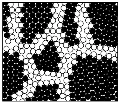
In other words, in the cores of interfaces and in the cores of other defects as well, the atomic structure, the electronic structure and the chemical composition of solids are modified in ways that differ from other structures of solid matter such
as glassesetc. The physical reasons for these modifications are the constraints excerted by the strained crystal lattice (surrounding any defect) on the matter inside the defect core (cf.Fig. 1). It is the basic idea1,2)of nanocrystalline solids to generate solids of novel atomic and electronic structures as well as novel chemical compositions - and hence novel properties - by incorporating so many interfaces (and/or other types of crystal defects) that the fraction of atoms situated in the cores of these defects becomes comparable to the fraction of atoms in the (strained) crystalline regions between the defects (Fig. 3). Solids with this microstructure are called nanocrystalline solids. Nanocrystalline solids seem to open the way to study and probably utilize a yet little explored -state of solid matter: the constrained -state of solid matter that exists in the cores of defects. However, the high density of defect cores not only modifies the atomic structure as well the chemical composition and reduces the crystal size to a few nanometers. The high defect density also leads to a modification of the electronic structure. Hence, in nanocrys-talline solids all four parameters controlling the properties of a solid (atomic structure, electronic structure, chemical composition and crystal size) are modified resulting in properties that are yet fairly unexplored. In the past decade, experimental as well as theoretical studies have been performed to test these ideas. An encyclopaedic review of the results reported so far seems to be beyond the scope of this paper. In this paper, we shall focus here on the deviation of the electronic structure of nanocrystalline materials from the electronic structure of a coarse-grained (or single crystal-line) materials with the same chemical composition. Con-cerning overview articles in which the atomic structure of nanocrystalline materials are treated, we refer to the follow-ing references.5–12)
One reason for the different electronic structure of nanocrystalline materials relative to coarse-grained or single crystalline materials is the electronic space charge at the contact region (Fig. 4) between chemically dissimilar
Fig. 1 Atomic arrangement in the vicinity of an edge dislocation in a simple cubic crystal. In the core of the dislocation, the interatomic spacings and the coordination between nearest-neighbour atoms is changed.
Fig. 2 Atomic structure in the core of a grain boundary between two NiO crystals. The atomic structure shown has been deduced from high-resolution electron microscopy. In the boundary core, the average atomic density is reduced and the coordination between nearest-neighbour atoms is changed (pentagonal and triangular structural units indicated by broken lines in the boundary core, whereas the crystal structure is cubic).3)
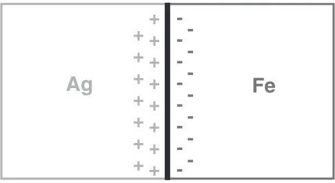
[image:2.595.92.246.69.211.2] [image:2.595.91.246.281.413.2] [image:2.595.328.521.541.708.2]crystals, provided these crystals have mobile charge carriers (i.e. metals, semiconductors). The thermodynamic equili-brium at an interface of this kind requires the electrochemical potential on both sides of the interface to be identical. In the case of an interface (frequently called a heterophase boundary) between two crystals with different chemical compositions (e.g.between an Ag and Fe crystal, Fig. 4), the chemical potential difference is balanced by an electrostatic potential in the form of an electrically charged layer on either side of the heterophase boundary (the so-called space charge layer, Fig. 4). These built-in space charges at heterophase boundaries may be utilized to generate materials the electronic structure and hence the properties of which deviates from the electronic structure (and the properties) of the regions far away from the space charge zone (e.g.
inside of the Ag and Fe crystals, respectively in Fig. 4). In order to generate solids the properties of which are controlled by the space charge regions, one has to incorporate such a high density of space charge regions (by means of a high density of heterophase boundaries) that the volume fraction of the space charge region approaches 50% or more of the total volume of the material. In fact, a volume fraction of 50% or more of electrically charged material is achieved, if the crystal size of a polycrystalline material (consisting of equal volume fractions of crystals with different chemical compositions and similar size) becomes comparable to the width of the space charge region which is in metals one nanometer or less. Thus, in the case displayed in Fig. 4, the size of the Ag and Fe crystals has to be reduced to a diameter of a few nanometers. Polycrystals made up of nanometer-sized crystals with different chemical compositions are called nanocomposites. Direct evidence of the intrinsically electri-cally charged state of nanocomposites due to space charge effects has been obtained,13) for example, from optical measurements (Fig. 5). The extinction observed for 2 nm Ag crystals embedded in a C60-matrix suggests that the 2 nm Ag crystals are electrically charged by about 0.2 electrons per Ag atom (curve C in Fig. 5). In the case of a Pd/Fe heterophase boundary (cf. Fig. 4), the space charge regions between chemically different partners has been revealed14) directly (Fig. 6) by means of Conversion Electron Mo¨ssbauer Spectroscopy.
2. Electronic Tuning of the Chemical and Physical Properties of Elements
Let us start by addressing the question: what is the significance of the space charge region for the electronic structure of metallic nanocomposits.
Figure 5 displays a nanocomposit that consists of the Ag and Fe crystals. Every Ag/Fe interphase boundary is accompanied by a space charge region with a thickness in the order of 0.5 nm. Hence if the crystal size of a nanocomposit is 3 nm or less, the fraction of atoms with a modified number of electrons per atom (i.e.atoms located in the space charge regions) is in the order of 50% or more. As there exists a close relationship between the number of electrons and the chemical properties of an element (or a
-+
+
+
+
+
+
+
+
-Fe
Ag
+
+
+
+
+
+
+
Fig. 4 Space charge at a heterophase boundary between Ag and Fe.
Fig. 5 Measured optical absorption of silver clusters embedded in a solid C60-film.13)For analysis, Mie spectra were calculated (curve A) with bulk dielectric properties of Ag, and if the conduction electron density in the silver clusters is reduced by 20% relative to the one in bulk Ag (curve C).
[image:3.595.47.290.71.204.2] [image:3.595.340.512.71.283.2] [image:3.595.327.520.353.514.2]chemical compound with mobile charge carriers), the chemical properties in the space charge regions deviate from the ones of the uncharged regions in the center of the crystallites. Specifically in the case of Ag and Fe (Fig. 7), the positive/negative space charge of Ag/Fe reduces/increases the density of the electrons in the Ag and in the Fe crystals by about 0.2 electrons per atom, respectively. In general, the prediction of the variation of the chemical and physical properties due to the space charge requires detailed con-siderations based on the modified electron wave functions in the charged regions. However, it may be speculated that the following, naive picture may give us a guideline for the charge-induced property variations. This picture is based on the periodic table of the chemical elements. In the space charge region indicated in Fig. 7, the number of electrons per Ag atom is reduced by about 0.2 electrons per Ag atom. This reduction is proposed to modify the electronic structure of Ag in such a way that the Ag atoms in this region change their chemical properties in the sense that they behave somewhat similar to Pd. Pd is the element in the periodic table with one electron per atom less than Ag. Obviously, this is a drastic oversimplification of the actual situation because the elec-tronic wave functions of Agþand Pd are different. In the case of Agþ the wave function is obtained by solving the Schroedinger equation for the potential of the Ag nuclei. In the case of Pd the wave function follows from the solution of the Schroedinger equation - for the same number of electrons - but for the potential of the Pd nuclei. In the framework of this oversimplified picture, the negatively charged (charge 0.2 electrons per Fe atom) is proposed to be electronically modified in such a way that its chemical properties approach Co (Co is the element which has one electron per atom more than Fe). Despite of its oversimplification this interpretation seems to indicate at least qualitatively in which way Ag and Fe are chemically modified by the electric charge in the space charge regions of Fig. 7. Electrically neutral Fe and Ag are known to be immiscible in the solid state whereas Pd and Co form continuous solid solutions, when alloyed in the electrically neutral state. Hence, in terms of the above oversimplified picture, one might speculate that the space
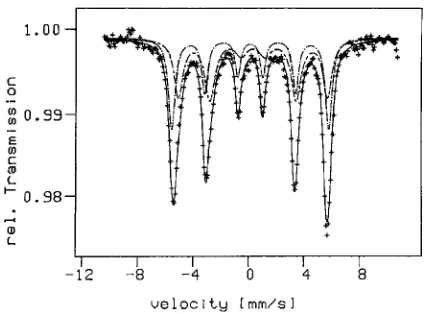
charge at the Ag/Fe interphase boundaries enhances the solid solubility of Ag and Fe because it modifies them chemically so that they have chemical properties that are ‘‘between’’ Ag and Pd or Fe and Coi.e.‘‘between’’ the (electrically neutral) elements of the periodic table, respectively. If this is so, it might be speculated that the electrically charged regions of the Fe and Ag crystals exhibit an enhanced mutual solute solubility. Such an enhancement of the solute solubility in the space charge region was, indeed, experimentally revealed.15) The Moessbauer spectrum (shown in Fig. 8), together with the results of X-ray diffraction experiments, indicates that in a region (about 4 atomic layers thick) on both sides of the interphase boundaries between the Ag and the Fe crystals, a Ag–Fe solid solution is formed (Fig. 9) as one would expect in terms of the oversimplified model outlined above. Naturally, if this interpretation of the experimentally ob-served enhanced solubility of Ag and Fe at Ag/Fe interphase boundaries is at least qualitatively correct, it should apply to other metallic nanocomposits as well. More specifically, the space charge should affect the mutual solubility of those nanocomposits consisting of metallic or semiconducting components with deviating Fermi energies. The deviation of the Fermi energies between adjacent metal crystals is well known to control the electric charge distribution in the space
Fig. 7 Space charge distribution in a nanocomposit consisting of nm-sized Ag and Fe crystals. At the heterophase boundaries between Ag/Fe-crystals space charge regions are formed (similar to Fig. 4). If the crystal size is comparable to the thickness of the space charge regions, a large volume fraction of the Ag and Fe atoms are located in the electrically charged regions.
Fig. 8 Moessbauer spectrum (-+-+-+-) of a nanocrystalline Fe–Ag alloy (30 at% Fe, 10 K, crystal size 8 nm). The spectrum contains of the following two components. Fe atoms dissolved in the Ag-crystals (---) and Ag atoms dissolved in-Fe-crystals (- - -).15)
[image:4.595.64.276.72.218.2] [image:4.595.320.532.382.539.2] [image:4.595.350.507.614.726.2]charge regions. In fact, in a recent survey16)covering metallic alloy systems with no measurable equilibrium solubility in the solid state were studied. The study revealed a correlation between the difference between the Fermi energies of the two constituents and an enhanced solubility in the nanocrystalline form. All 21 alloy systems studied had the following two features in common. They exhibited (i) a large difference between the Fermi energies, EF, of both constituents (EF>1eV). This large difference results in the formation of a space charge at the heterophase boundaries. (ii) The elements in the periodic table toward which the two constituent elements of the nanocomposit where ‘‘shifted’’ in terms of their electron density per atom by the space charge, are known to form solid solutions (Similar to Pd and Co in the case of Ag and Fe, in the sense discussed above). Alternatively, the enhanced solute solubility of nanocompo-sites has been interpreted in terms of the entropy driven mixing of the components or in terms of the local elastic strains introduced if nanocomposites are produced by severe plastic deformations, e.g. by ball milling.33) Both models suffer from the fact that typical enthalpies of mixing are at least one order of magnitude larger (103. . . 104J/mol) than the contributions from the entropy of mixing (at 500 K about
102. . . 103J/mol) as well as the energy stored in the heavily deformed materials (about 100. . . 101J/mol).16)Clearly, the
solute solubility of metals (and semiconductors) is only one facet of the world of phase equilibria. An other, well known class of phases that is based on the relationship between the electronic and atomics structure of metals, are the so called electron phases. About 75 years ago, Hume-Rothery indicted the possibility that certain phases possess the same crystal-lographic structure if the number of valence electrons per atom, e=a, are comparable (electron phases). In fact, for example, the -brass structure was found to be associated withe=a¼1:50, whereas the-brass and"-brass structures corresponded to 1.62 and 1.75, respectively. As was pointed out previously, in metallic nanocomposites, the electronic structure in a relatively large volume fraction of the material differs from the one of the bulk due to space charge effects. Hence, if one or several of the components of a nanocompo-site are Hume-Rothery phases, the deviation in the electronic structure in the space charge regions may render the structure of the Hume-Rothery phases unstable and transforms them into structures that correspond to the local (e=a) values inside of the space charge region.
So far, the discussion was focused on the variation of the alloying behaviour and on the phase stability of metals due to the modification of the electronic structure. However, the modification of the electronic structure appears unlikely to affect only the alloying behaviour as well as to the phase stability. In fact, the modification of the electronic structure may open the way into a new area of Solid State Chemistry and Physics: the Chemistry and Physics of electrically highly charged solids. Or, in other words, metallic or semiconduct-ing solids that are - in terms of their electron density per atom - ‘‘between’’ the - electrically neutral - elements of the periodic table.17,18) In order to explain this idea, let us consider a nanometer-sized Cu crystal. If this crystal is electrically charged with, say, 0.1, 0.2. . .electrons per Cu-atom, the average density of electrons per atom in the crystal
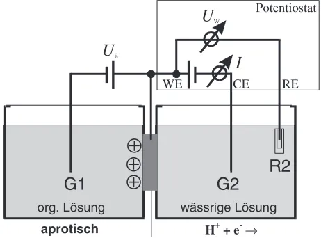
changes. This change of the density of electrons may be expected to modify all chemical and physical properties that depend on the electron density. In other words, we may be able to tune all these chemical and physical properties by tuning the electron density. This idea has been tested by utilizing the model system Pd–H.19) If a (an electrically neutral) Pd-crystals is immersed into an atmosphere of hydrogen with a constant pressure of hydrogen, a certain amount of hydrogen will be dissolved in the Pd crystal. In a simplified picture, the hydrogen dissolution may be thought of to occur by the following process. Once a hydrogen atom diffuses into the Pd crystal, the electron of this hydrogen atom enters the conduction band of the Pd crystal and the remaining hydrogen ion is incorporated into the Pd lattice as an interstitial atom. The concentration of the dissolved hydrogen in the Pd crystal depends - for any given chemical potential of the hydrogen - on the number of electrons that can enter the conduction band of the Pd. If this is so, then the maximum concentration of hydrogen that can be dissolved in a Pd crystal (at any given hydrogen pressure) will depend on the number of unoccupied electronic states in the conduction band of Pd. Consequently, if we remove electrons from the conduction band of a Pd crystal by charging it positively before exposing it to the hydrogen atmosphere, we may expect that this positively charged Pd crystal can dissolve more hydrogen than an uncharged Pd crystal at the same hydrogen pressure. The unoccupied electron states created in the conduction band of Pd by the electric charging process may allow additional hydrogen atoms to be dissolved. The electrons of these additionally dissolved H atoms can enter into the unoccupied electronic states created in the conduc-tion band of Pd by the electric charging. The opposite effect is expected to result when additional electrons are injected into the conduction band of Pd by charging the Pd negatively prior to dissolving the H. In other words, we may be able to modify the chemical properties of Pd by charging it electrically prior to the reaction with the hydrogen. This expected correlation between the electric charging and the chemical behaviour of Pd agrees with the following experi-mental observations.19) In order to test these ideas, an experimental arrangement as shown in Fig. 10 was used. It
org. Lösung
aprotisch
wässrige Lösung
U
aI
U
wG1
G2
R2
Potentiostat
RE CE
WE
H+ + e
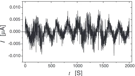
[image:5.595.310.541.587.758.2]consists of two electrolytes that were separated by thin film of Pd. One of the electrolytes (on the left side of the Pd film, Fig. 10) was an organic electrolyte. This electrolyte was used to charge the left surface region of the Pd film positively or negatively by means of an applied voltage,Ua. The aqueous electrolyte on the right side of the Pd film (Fig. 10) provided hydrogen with a constant chemical potential. Let us now assume that the electron density in the Pd-conduction band of the surface region on the left hand side of the Pd film (Fig. 10) is increased/decreased by means of the applied voltage,Ua. Hence according to the above discussion, we expect the hydrogen solubility in this electrically charged surface region to decrease/increase. This speculation was tested experimen-tally as follows. In the beginning of the experiment, the system (Fig. 10) was equilibrated at constant temperature and with an electrically neutral Pd film (i.e.Ua¼0). In this state, the Pd dissolved a certain amount of hydrogen. Then the Pd film was negatively charged in its surface region by means of applying a negative voltage (Ua in Fig. 10). Let us now assume that in the negatively charged surface region of the Pd film, the solute solubility for hydrogen is reduced. If this assumption is correct, the Pd surface region is supersaturated with hydrogen. The excess hydrogen can leave the negatively charged surface region of the Pd film by diffusing (through the electrically neutral regions of the film) into the aqueous electrolyte on the right hand side of the Pd film. After 100 s the electric surface charge of the Pd film was inverted by applying a positive voltage,Ua. This inversion is assumed to increase the solute solubility of hydrogen in the electrically charged surface region of the Pd film. If this assumption is correct, the additional hydrogen that may now be dissolved in the positively charged Pd surface region is supplied by the aqueous electrolyte: In fact, this enhanced solubility will result in a driving force which causes the hydrogen to enter the Pd film from the aqueous electrolyte, diffuse through (the electrically neutral part of) the Pd film and become incorporated into the positively charged surface region of the Pd film. This hydrogen flux from the Pd film into the aqueous electrolyte (when Ua<0) or from the aqueous electrolyte into the Pd film (whenUa>0) may be monitored by means of the electric current,I, between the electrode G2 and the Pd film (Fig. 10). However, if - contrary to the above discussion - the hydrogen solubility would be unaffected by the electric charge in the Pd film, no current will be noticed. Figure 11 shows the current,I, if the polarity of the voltage,
Ua, is inverted every 100 s. As may be seen from Fig. 11, the hydrogen solubility of Pd does indeed depend on the electric charge in the Pd film. Although the direction and the magnitude of the current noticed seems to agree with the expected direction/magnitude, it should be pointed out that the hydrogen solubility of organic electrolytes is small but not zero as was assumed so far. This small solubility may depend onUa. In other words, the current,I, shown in Fig. 11, may be affected by this effect, as well. Using a slightly different experimental arrangement than the one shown in Fig. 11, this effect is presently studied. There is, however, already now one observation which suggests that the picture presented above, describes the process reasonably well. If the above ideas are basically correct, a variation of the hydrogen concentration in the Pd film is achieved by the diffusion of
the hydrogen from the electrically charged surface region of the Pd film through the entire volume of the film into the aqueous electrolyte and vice versa. Hence, the time required to charge/discharge the surface region of the Pd film with hydrogen would be the time required for the diffusion of the hydrogen through the Pd film. This correlation between the film thickness and the time required for the charging/ discharging of the film seems to agree with the experimental observations. However, if the hydrogen would enter/leave the Pd film from/into the organic electrolyte, the diffusion time is expected to be much shorter and would be independant of the thickness of the Pd film. This was not noticed to be so. The idea of a relationship between the electron density and the chemical properties - here, specifically the hydrogen solute solubility in Pd- is also supported by other observations.20) The hydrogen uptake in superlattices consisting of alternating layers of Mo and V single crystals was measured by profiling the hydrogen concentration within these films as a function of the distance from the Mo/V interfaces. This profiling was performed by using the 1H (15N,) 12C reaction and X-ray diffraction experiments. Super lattice films with different modulation wavelengths,, that were varied between 0.3 and 17.7 nm were used. The average ratio of hydrogen to metal was found to decrease ifwas reduced. This decrease was shown to result from a reduced hydrogen solubility in the V crystal lattice in a region adjacent to the Mo/V interfaces. The thickness of the regions of reduced hydrogen solubility was found to be about 0.49 nm. The reduced hydrogen solubility in V near the Mo/V interfaces was interpreted in terms of the electronic space charge in V near the Mo/V interfaces. In fact, the reduced hydrogen solubility in the vicinity of the Mo/V interfaces was used to estimate the variation of the electron density, due to the space charge. An increase of the electron density by about 23% was obtained, if the strains due to the lattice mismatch between Mo and V were assumed to have no effect on the hydrogen solubility in V.20)
An obvious technological application of the modification of the solid solubility of hydrogen in metals by an externally applied voltage seems to be a storage tank for hydrogen. The storage capacity of this tank may be tuned by an externally applied voltage. This kind of a tank would have the advantage that hydrogen charging or discharging could be controlled by varying the applied voltage. In all hydrogen storage devices available today, the charging/discharging is
0 500 1000 1500 2000
-0.010 -0.005 0.000 0.005 0.010
I
[
µ
A]
t
[S]
[image:6.595.310.546.71.204.2]performed by varying the temperature.
Clearly an excess electric charge may not only expected to modify many chemical properties of metals and semicon-ductors, it may also be expected to affect numerous physical properties.
For reasons of brevity, this paper will be limited to three examples of this kind: the charge induced variation of the interatomic spacing, of the electric conductivity and of the optical properties.
3. Charge Induced Variation of the Interatomic Spacing
In simple, electrically neutral metals,21) the interatomic potentials consist (in the pair-potential picture) of a hard core repulsive contribution, an attractive nearest neighbour com-ponent and an oscillatory long-range potential. In transition metals, the cohesive energy and the crystal structure is dominated by the d-bond contribution. In metals deviating to an increasing extent from charge neutrality, the Coulomb repulsion between the ion cores will become more and more dominate for the interaction potential. Thus, the Coulomb repulsion will affect the crystal structure with increasing deviation from charge neutrality. The crystal structures corresponding to the electrically highly charged state may be frozen-in by heating highly charged nanometer-sized crystals to elevated temperatures. At elevated temperatures, they may (e.g. by diffusive processes) transform into the crystal structure corresponding to the charged state. This new structure may be preserved by cooling the charged, structu-rally transformed crystallites to low temperatures. Direct evidence for the coupling between the interatomic forces and the deviation from charge neutrality was recently obtained by measuring the lattice constant of 10 nm Pt crystals as a function of their excess electric charge.22)The experimental arrangement used is shown in Fig. 12. Inter-connected electrically conducting arrays of metallic nanoparticles with a large surface-to-volume ration immersed in an electrolyte are used as an electrode and counter electrode, respectively. Upon applying an external voltage, typical charge densities of 0.3 C/m2 can be achieved in this way at the metal-electrolyte interfaces. The thickness of the layer over which the excess electric charge in the metal is distributed corresponds to the electronic screening length in metals.
This is roughly one or few interatomic spacings. It is readily estimated17) that the extra charge which can be reversibly added or withdrawn from the nanometer-sized crystals shown in Fig. 12 corresponds to about 0.2 electron per atom in the first atomic layer at the surface. Some measurements in the literature indicate even higher charges/atom.13)
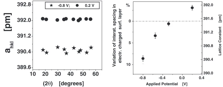
This charge modifies the local electronic structure as it corresponds to a substantial local deviation from charge neutrality. One of the interfacial properties which depends on the local electronic structure is the interface stress,S. When the area is measured in coordinates of the undeformed crystal lattice, thenS is phenomenologically defined as the deriva-tive of the interfacial free energy with respect to the strain,E, tangential to the interface. Microscopically, the interface stress reflects the tendency of the surface to energetically favour a lateral interatomic spacing that differs from the one of the underlying bulk. The growing body of data on the stress associated with the surface between a single crystal and the vacuum and attempts to understand its relationship to the electronic structure of the surface, were reviewed by Ibach.24) In order to study the variation of the lateral interatomic spacing as a function of the variation of the modified electronic structure of the free surface due to the applied external electric potential, X-ray diffractograms were recor-dedin-situat different applied potentials. Figure 13(a) shows the ‘‘effective lattice constants’’,ahkl, computed by applying
Bragg’s law individually to each Bragg reflection of the nanometer-sized Pt crystallites, after utilization the Nelson-Riley correction for sample displacements along the scatter-ing vector. The variation ofahklwith the diffraction angle,2,
is much smaller than the voltage-induced mean strain (Fig. 13(a)). This suggests that, the strain is isotropic and accurately measurable. Figure 13(b) displays the voltage-induced variation of the lattice constant (Scale on the right hand side of Fig. 13(b)). The maximum variation of the lattice constant is about 0.4%. It is found to depend non-linearly on the potential, with the largest slope at more negative potentials (Fig. 13(b)). The variation of the lattice constant is reversible upon variation of the applied voltage. Moreover, its value is found to remain unchanged when the potential is maintained for long durations (36 h). In terms of the ideas discussed above, the observed variation of the lattice constant (Fig. 13(b)) as a function of the applied potential is caused by the variation of the interatomic spacing in the thin surface layer of the crystallites due to the variation of the electronic structure in this layer. If the variation of the electronic structure results in a reduction of the interatomic spacing in the surface layer, this layer contracts and, thus, compresses the interior of the crystallites hydrostatically. This hydrostatic compression is evidenced by the observed variation of the lattice constant (Fig. 13(b)). If this is so, one might ask the question: what would be the reduction of the interatomic spacing in the charged surface layer, if this layer would have the shape of a hollow shell with the thickness of the electrically modified region. In other words, it is assumed that the surface layer would not have to compress the interior of the crystallites. In fact, the surface layer is assumed to contract freely. Assuming a shell model of this kind, based on linear elasticity theory and assuming, moreover, constant elastic moduli and a thickness of the shell (surface layer) of
[image:7.595.74.262.618.729.2]X-ray
0.25 nm, one finds (assuming a diameter of the crystallites of 10 nm) a remarkable large, charge induced contraction of up to 10% of the interatomic spacing in the shell (Fig. 13(b), scale on the left hand side). Since the compression excerted by the shell on the interior of the crystallites is isotropic, the pressure inside of the crystallites (due to the variation of the interatomic spacings in the electronically affected surface layer) may be estimated from the measured volumetric strain. If a is the measured variation of the lattice constant (Fig. 13(b)), the volumetric strainV=Vo¼3a=aowhereaois the unstrained lattice constant. In the framework of linear elasticity, the change in the pressure inside of the Pt crystallites is related to the volumetric strain by
hPiv hP0iv¼ KðVV0Þ=V0
whereKdenotes the Bulk modulus,K¼276GPa for Pt, and the brackets refer to volumetric averages. The subscript ‘0’ refers to the pressure and the interface stress in the reference state, which we have chosen to be the dry powder. By inserting the numbers given above, one finds the pressure reaches values as high as 3.2 GPa.
Hydrogen adsorption and electrocapillarity have been ruled out22) as the microscopic origin of the observed variation of lattice constant. Hence, one is lead to conclude that the observed variation of the lattice constant is determined by changes in the electronic structure of the surface. Although no simple quantitative relationship be-tween the variation of the lattice constant and the electronic structure is known, it is reasonable to assume that an increase of the surface charge density of transition and noble metals increases the surface stress.24)This expectation is based on the concept that the charge is accumulated between the surface atoms in the form of a bond charge, and that extra electrons will increase the charge density in these bonds, thereby making the in-plane bonds more attractive. These attractive interatomic interactions in the surface region must be balanced by a more compressive (i.e., more negative) stress in the bulk of the Pt crystallites. This implies immediately a more positive nature of the surface stress. This notion is generally applied to understand the positive
value of the surface stress of clean metal surfaces: when a surface is created in a infinite crystal by cutting the atomic bonds across the plane of the surface, then the corresponding bond charges are relocated into the plane of the newly formed surface, thereby injecting extra electrons into the parallel bonds. In our experiments, the analogous effect is achieved by increasing the electron density in the double layer as a consequence of applying negative potentials. The present findings for the variation of the interatomic spacing are qualitatively compatible with the above concept.
[image:8.595.102.492.72.225.2]One potential technological application of this effect seems to be cantilever-type actuator. A schematic drawing of one of the conceivable actuator designs is shown in Fig. 14. The actuator consists on one side of a thin Pt film which is coated by a layer of nm-sized Pt crystals. These nm-sized Pt crystals are electrically and mechanically interconnected so that a sponge like structure results similar to the one shown in Fig. 12. In order to operate the actuator, the actuator is immersed into an electrolyte. This electrolyte penetrates into the free volume between the nm-sized Pt-crystals of the
10 20 30 40 50 60 389.6
390.4 391.2 392.0 392.8
a
hkl[pm]
(2θ) [degrees]
-0.8 V; 0.2 V
-0.8 -0.4 0.0 0.4 10
5 0
%
Lattice Constant [pm]
Variation of interat. spacing in electr. charged surf. layer
Applied Potential [V]
390.0 390.4 390.8 391.2 391.6 392.0
Fig. 13 Left side: Effective lattice constant,ahkl, of 10 nm Pt crystals determined from respective Bragg reflections, after Nelson-Riley
correction for sample displacements along the scattering vector.2: scattering angle, dots:E¼ 0:8V; stars:E¼ þ0:2V.Eis the applied potential. Right side: lattice constant (right ordinate). Dashed line: lattice constant of the dry powder, used as the reference for computing the strain. Left ordinate: computed variation of the lattice constant of a hollow shell of Pt (shell thickness 0.25 nm, diameter 10 nm), if the shell is electrically charged in the same way as the 10 nm Pt crystals (left side of Fig. 13).
[image:8.595.306.548.568.730.2]sponge. If the actuator is electrically charged (Fig. 14) relative to a reference electrode, the length of the Pt film will remain essentially unchanged. However, the length of the Pt sponge expands or contracts according to Figs. 12 and 13. The main advantages of such an actuator seem to be as follows. The actuator requires no intercalation as do actuators based on faradic conducting polymers. In comparison to ferroelectric actuators, it has a lower operating voltage and a higher work density. A similar actuator based on carbon nanotubes was recently proposed by Baughman.25)
Naturally, apart from lattice constant variations, other properties are expected to vary as well when solids deviate from charge neutrality. In order to keep the length of this paper within the desired limits, we shall focus on only two more types of charge induced property variations: electrical and optical charge induced property variations charge induced variation of the electric conductivity.
Technologically, the most important example of the controlled enhancement or depletion of the local density of charge carriers by applying an external voltage seem to be field effect transistor (FET) devices. These devices consist of a source/drain electrode on opposite sides of a doped (e.g.a p-doped) semiconductor crystal and one (or two) gate electrodes on the side surfaces, Fig. 15. The insulation between the gate electrode and the semiconductor crystal may be achieved either by a thin oxide (mostly SiO2) layer (MOSFET) or by n-doping a thin region next to the gate (if the semiconductor is p-doped). The flow of electrons between the source and the drain electrode depends on the density of electrons in the p-doped semiconductor. A negative potential between the gate and the drain, creates a high charge carrier density near the gate and, thus enhances the conductivity of the semiconductor. A positive potential between the gate and the drain reduces the charge carrier density and, hence, the conductivity. The same principle was recently applied23)in order to tune the dc-conductivity of a carbon fibres that are immersed in a monomolar NaCl electrolyte. By varying the potential applied between the carbon fibres and the electro-lyte, the carrier density in the fibres was changed. The resistivity of the carbon fibres was noticed to vary if the fibres were charged positively or negatively (Fig. 16). This result may be understood as follows: the electric resistivity of a solid is essentially controlled by two factors, the density of the mobile charge carrier as well as by their mean free path. If
the mean free path of the charge carriers in the carbon fibres is assumed to depend little on the charge carrier density, the resistivity should vary proportional to the density of mobile charge carriersi.e.the density of states at the Fermi energy. In the case of the carbon fibres, the density of the states increases if the Fermi energy is increased or decreased relative to the electrically neutral state by applying an external potential. Hence the dc resistivity of the electrically neutral carbon fibres should be higher than the resistivity of the positively as well of as of the negatively charged carbon fibres, as was observed (Fig. 16).
4. Charge Induced Variation of Optical Properties
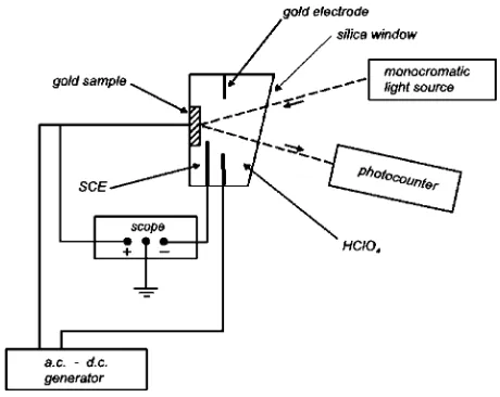
[image:9.595.323.530.72.267.2]An experimental set-up that allows one to study the variation of the optical reflectivity of metals upon applying an external voltage is shown in Fig. 17. The applied voltage between the gold sample and the reference electrode (connected to the a.c./d.c. generator) induces a change of the free electron density at the surface of the gold crystal
Fig. 15 Silicon metal-oxide-semiconductor field effect transistor (MOS-FET). Schematic diagram of the device.
-1.0 -0.5 0.0 0.5 1.0 150
200 250 300 350 400 450
Resistance [ohms]
[image:9.595.311.541.577.760.2]Applied Potential, [V]
Fig. 16 DC resistivity of a graphite fiber immersed in a 1 molar aqueous solution of NaCl as a function of the applied potential.23)
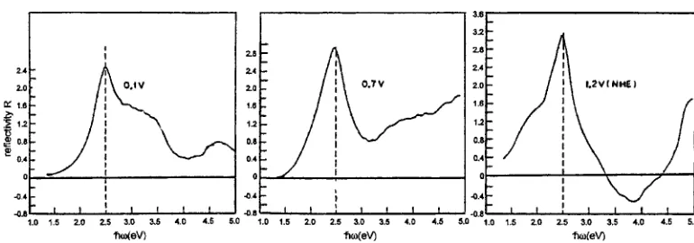
[image:9.595.62.277.626.760.2](Fig. 17). As the plasmon frequency of a metal crystal with (nearly) free electrons depends on the square root of the electron density27,28) the metallic reflectivity e.g. of gold, may be changed reversibly by means of the applied voltage (Fig. 18). Metals as well as semiconductors with tuneable reflectivity may be of technological interest,e.g.for displays, switchable mirrors, windows with adjustable transparency for sun-light, optical filtersetc.
So far, switchable mirrors (i.e. mirrors the reflectivity of which can be tuned by varying an external parameter) have been produced by exposing a thin (500 nm) film of Y to an atmosphere of hydrogen.29)At low H2 pressures (103Pa or less), the Y is in the metallic state and, thus, the reflectivity for visible light is high (nearly 100%). If the H2 pressure is increased, YHxforms. Forx>2(i.e.compositions between
YH2 and YH3), the YHx becomes transparent for visible
light. By modulating the hydrogen pressure between105and
60105Pa, YH
x mirrors may be switched between a
reflective and a transparent mode. According to the model of Nget al.30)this behaviour may be understood in terms of the hydrogen induced modulation of the electronic band structure of YHx. YH3 (1) may be considered as a semiconductor with localized donor states. Each donor state corresponds to one hydrogen vacancy. As long as the average spacing of the donor states is larger than the radius of the donor wave function, the material is transparent. For (0:15) the spacing between the donor states becomes so small that their wave functions start to overlap. As a consequence, YHx forms a conduction band and starts to exhibit metallic reflectivity. Clearly, the tuning of the electronic band structure caused by the variation in the chemical composition (in the case of YHx by varying the
hydrogen content) it may not be the only approach. The tuning of the band structure may also be achieved by an applied electric field or by injecting excess charges into an electrically neutral solid. An example is shown in Fig. 19. The absorption spectrum of silver nano-particles31,32) ex-periences a number of changes if excess electrons or excess (positive) holes are stored. Figure 19 displays the spectral changes around the 380 nm plasmon absorption band of the silver particles, when excess electrons and excess holes are deposited. The experiments were carried out by generating reducing or oxidizing radicals in a silver sol by a short pulse of radiation and measuring the optical changes after 5 ms
[image:10.595.103.488.67.202.2](when all radicals generated had reacted with the silver particles).31) The strong increases and decreases in optical absorption which occured on the two flanks of the 380 nm plasmon band of the silver particles indicate that the band is shifted towards shorter wavelengths upon electron (and to longer wavelengths upon positive hole) injection. The theory, indeed, predicts these shifts, as the wavelength of the band maximum is proportional to the reciprocal square root of the free electron density in the silver particles.32)In addition, one observes a small absorption decrease or increase at small wavelengths range around 300 nm. In this range, the first 4d!5s transitions occur in metallic silver particles. When the Fermi level energy is increased by excess electrons, the threshold for the interband transition is blue-shifted, resulting in negative signals in the pulse experiment of Fig. 19.
Fig. 18 Reflectance,R, of Au as a function of the frequency,!, of the light at 45incidence measured at various potentials for in a 0.5 kmolm3H
2SO4electrolyte. The curves indicate the reflectance if the light polarization is parallel to the free surface of the Au crystal,26)cf.Fig. 17. h is Planck’s constant.
[image:10.595.332.522.264.481.2]REFERENCES
1) P. Marquardt and H. Gleiter: Verh. d. Deutsch. Phys. Gesellsch.15
(1980) 328.
2) H. Gleiter: Proceed. Second Ris Internat. Symp. On Metals and Materials Science, Eds.: N. Hansen, T. Leffers and H. Lilholt, Roskilde, (Riso National Lab. Roskilde, Publ. Denmark 1981) p. 15.
3) K. L. Merkle, J. F. Reddy, C. L. Wiley and D. J. Smith: Phys. Rev. Lett.
59(1989) 2887.
4) E. D. Hondros, M. P. Seah and P. Lejcek:Interfacial and Surface Microchemistry in: ‘‘Physical Metallurgy’’, Eds. R. W. Cahn and P. Haasen, (Fourth Edition, Elsevier Science B. V. Amsterdam, 1996) 1202.
5) R. Dagani: Chem. and Eng. News70(1992) 18. 6) H. Gleiter: Progr. Mater. Sci.33(1989) 223. 7) H. Gleiter: NanoStruct. Matls.1(1992) 1.
8) G. C. Hdjipanayis and R. W. Siegel in:Nanophase Materials, Eds. G. C. Hdjipanayis and R. W. Siegel, (Kluwer Acad. Publ. Dordrecht, Netherlands, 1994).
9) R. W. Siegel in:Encyclopedia of Applied Physics, Vol. 11 Ed.: G. L. Trigg, (VCH Weinheim, Germany 1994).
10) C. Suryanarayana: Int. Met. Rev.40(1995) 41.
11) J. Weissmu¨ller in: Synthesis and Processing of Nanocrystalline Powder, Ed. D. L. Bourell, (TMS Publ. Warrendale Pa., 1996) p. 3. 12) R. Z. Valiev, R. K. Islamgaliev and I. V. Alexandrov: Progr. Mater. Sci.
45(2000) 104.
13) U. Kreibig, G. Bour, A. Hilger and M. Gartz: Phys. Status Solidi a.175
(1999) 351.
14) G. Kisters, Ch. Sauer, E. Tsymbal and W. Zinn: Hyperfine Interactions
92(1994) 1285.
15) U. Herr, J. Ying, U. Gonser and H. Gleiter: Solid State Commun.76
(1990) 192.
16) H. Gleiter and M. Fichtern: Scr. Mater.46(2002) 497.
17) H. Gleiter, J. Weissmu¨ller, O. Wollersheim and R. Wu¨rschum: Acta Mater.49(2001) 737.
18) H. Gleiter: Scr. Mater.44(2001) 1161.
19) D. Kramer and J. Weissmu¨ller: private comm. 2002.
20) B. Hjo¨rvarsson, J. Ryden, E. Karlsson, J. Birch and J.-E. Sundgren: Phys. Rev.B 43(1991) 6440.
21) D. G. Pettifor in:Physical Metallurgy, eds. R. W. Cahn and P. Haasen, Vol. 1, (North Holland Publ. Amsterdam, 1996) pp. 95.
22) R. N. Viswanath, J. Weissmu¨ller, R. Wu¨rschum and H. Gleiter: Mat. Res. Soc. Symp. Proc.676(2001) Y6.10.
23) R. N. Viswanath: private comm. (2001). 24) H. Ibach: Surface Science Reports29(1997) 193. 25) R. Baughman: Science284(1999) 1340.
26) R. Garrigos, R. Kofman and J. Richard: Nuovo Cimentao B1 (1973) 272.
27) H. Lu¨th:Surfaces and Interfaces of Solid Materials, 3rd Ed., (Springer-Verlag Berlin, 1995) pp. 268.
28) K. H. Hellwege:Einfu¨hrung in die Festko¨rperphysik, (Springer-Verlag Berlin, Heidelberg, 1976) p. 477.
29) J. N. Huiberts, R. Griessen, J. H. Rector, R. J. Wijngaarden, J. P. Dekker, D. G. de Groot and N. J. Koemann: Nature380(1996) 281. 30) K. K. Ng, F. C. Zhang, V. I. Anisimov and T. M. Rice: Phys. Rev. Lett.
78(1997) 1311.
31) A. Henglein: Ber. Bunsenges. Phys. Chem.101(1997) 1562. 32) W. T. Doyle: Phys. Rev.111(1958) 1067.
33) C. Suryanarayana: Prog. Mater. Sci.46(2001) 1.