High-Performance Quasi-Z-Source Series Resonant
DC-DC Converter for Photovoltaic Module Level
Power Electronics Applications
Miss Tejashri Wable
1, Dr. V. M. Panchade
21, 2Department of Electrical, G. H. Raisoni College of engineering and technology , Pune, India
Abstract: Presents the high-performance quasi-Z-source series resonant DC-DC converter as a candidate topology for the PV module level power electronics applications. The converter features a wide input voltage and load regulation range thanks to the multi-mode operation, i.e. when the shoot-through pulse-width modulation and phase-shift modulation are combined in a single switching stage to realize the boost and buck operating modes, respectively.
Keywords: resonant converter; DC-DC converter; quasiZ-source converter; renewable energy; solar photovoltaic; module level power electronics; module integrated converter (MIC)
I. INTRODUCTION
A two-stage topology is proposed, which consists of a boost converter and a SRC. The boost converter steps the changing PV voltage VPV to an intermediate constant voltage bus VDC,mid. The SRC converter is operated at fres,1 in half-cycle discontinuous conduction mode (HC-DCM). This enables a very efficient voltage conversion by utilizing the transformer leakage inductance as resonance inductance and the magnetizing current in combination with the parasitic output capacitances of the full-bridge MOSFETs for ZVS switching.A DC-to-DC converter is an electronic circuit which converts a source of direct current (DC) from one voltage level to another. It is a class of power 8 converter. The DC output voltage is controlled by varying duty cycle. There are three basic types of DC – DC converters considered for DC power conversion. These circuits are designed by using a semi conducting switch such as a thyristor, IGBT, GTO. The switch is turned on by a gate pulse (duty ratio). The switch is connected in series with the load to a DC supply, or a positive voltage is applied between the terminals. When the switch is turned off, the current flow decreases which is considered as below holding current, or a reverse (negative) voltage is applied between anode and cathode terminals. Therefore, proper gate pulses are required for obtaining the desired converter output.
[image:1.595.193.402.573.636.2]The impedance network provides an efficient result meaning that, the power conversion is between source and load in a wide range of electric power conversion applications (DC – DC, DC – AC, AC – DC, AC - AC). Various topologies and control methods using different impedance-source networks have been presented in the literature, e.g., for adjustable-speed drives, uninterruptible power supply (UPS) distributed generation, (fuel cell, photovoltaic (PV), the wind, etc.) battery or super capacitor energy storage electric vehicles. The general block diagram for impedance network is shown in figure1. With the switching configuration, it is possible for electrical power conversion application.
Fig 1 General circuit configuration of an impedance-source network
II. RELATED WORK
Zambra, D. A. B., et al., (2010) proposed “Comparison of NeutralPoint-Clamped, Symmetrical, and Hybrid Asymmetrical Multilevel Inverters.” This paper presents performance indexes such as total harmonic distortion, first-order distortion factor, second-order distortion factor, common-mode voltage, semiconductor power loss distribution, and heat-sink volume. Multilevel inverters are designed to present 99% efficiency at the nominal operating point. Basically, these types of structures require a large number of switches [1].
Qian, W., et al.,(2011) proposed “Trans-Z-source inverters.” The proposed inverter is constructed by using two inductors and capacitors 64 interfaced with DC source and the inverter bridge. This is possible for both buck and boost operation increased voltage gain and the voltage stress in the output waveform. It is a new bidirectional power flow based diode -impedance network for developing the reverse blocking IGBT. Thus wide range of voltage is obtained from various applications such as hybrid/electrical vehicles to other motor applications
Nguyen, M. K., et.al, (2012) proposed “Switched-Inductor Quasi-ZSource Inverters.” This paper proposes Switched-inductor quasi-Z-source inverters (SL-qZSIs). The proposed SL-qZS is based on the well-known qZSI topology and adds only one inductor and three diodes. In comparison to the SLZSI, for the same input and output voltages, the proposed SL-qZSI provides continuous input current, a common ground with the DC source, reduced passive component count, reduced voltage stress on capacitors, lower shootthrough current, and lower current stress on inductors and diodes [2].
Trinh, Q. N., et al., (2012) proposed “A new Z-source Inverter Topology with High Voltage Boost Ability.” This paper proposes a new Zsource inverter (ZSI) topology developed to improve voltage boost ability. The voltage gain ratio of SL inverter is high and very small shoot -through duty ratio. The volume and cost of the system are almost same as those of the conventional one. Harmonic current is produced across the inductor with inverter side. Large filters are required.
Nguyen, M. K., et al., (2013) proposed “TZ-Source Inverters.” This paper proposes a single-stage high-step-up boost voltage inverter based on transformers, called TZ-source inverters. This inverter produces a very high boost voltage gain when the turn ratio of the transformer is larger than one. This reduces the transformer’s size and weight while producing the same output voltage gain but the transformer windings produce voltage stresses.
Tang, Y., et al., (2013) proposed “Z-source AC-AC converters solving commutation problem.” In this paper, a Z-source AC-AC converter is presented to improve the buck-boost ability, which includes four switches in single phase and six switches in three phases. For safety purpose, a new communication strategy is used without using any snubber circuits. The results are verified both by simulation and experimental vice. These converters have more advantages and achieve low switching losses and less number of switches, therefore high efficiency and great reliability were achieved [3].
Reddy ,T. S., et al., (2013) proposed “Novel DC-DC Converter for PV system with High Voltage Gain.” This paper presents a new family of dc–dc converters based on the three-state switching cell and voltage multiplier cells. This includes the addition of a variable DC-DC converter placed between the array and the load. It is suitable for high voltage DC applications. The major advantages of this topology are the input current is continuous with low ripple; the input inductor is designed for twice the switching frequency, with consequent weight and volume reduction; the voltage stress across the switches is lower than half of the output voltage, and naturally clamped by one output filter capacitor. As a disadvantage, a small snubber is necessary for each switch and one additional winding per cell is required for the autotransformer [4].
Zengin, S.J, et al., (2013) proposed “Decoupling Capacitor Selection in DCM Flyback PV Micro inverters Considering Harmonic Distortion.” This paper focuses on the selection of minimum decoupling capacitor value for the proper operation of discontinuous conduction mode flyback PV microinverters by considering the total harmonic distortion (THD) and PV power utilization ratio. A decoupling capacitor selection method for single-stage and two-stage flyback inverters is proposed. For single-stage inverters, the decoupling capacitor is placed across the PV output terminals, and should be sized according to the desired THD limit. For two-stage inverters, the control method of the dc–dc converter determines the two-stage where the decoupling function takes place. 66 Thus, the PV side decoupling capacitor should be dimensioned according to the PV power utilization ratio, and the inverter side decoupling capacitor should be selected according to the desired THD limitation. It is noted from the proposed system output response of the input voltage of the PV module, drain to source voltage and switching pulse, transformer primary voltage and secondary voltages, input current, transformer secondary side current, output voltage, output current, and output voltage are reduced [5].
such as Perturb and Observe, Incremental Conductance, fuzzy logic based tracking technique. The P&O and Incremental Conductance are very old model algorithms and it has more drawbacks. The steady state operating point oscillates maximum region, it may be the wastage of power from the PV panel. But the fuzzy logic controller provides fast and stable tracking maximum power as compared with other control techniques. The major advantage of this scheme is that it measures the PV current perfectly [6]. Das, M., et al., (2014) proposed “A Novel Control Strategy for Standalone Solar PV Systems with Enhanced Battery Life.” A new control scheme ABC (three phase) to DC is proposed for a stand-alone PV application. There are two power converting stages used for high gain DC–DC operation, which is followed by three phase converter. The reactive power load is considered for PV based stand-alone application and the active power demand is controlled by regulating the dc link voltage. Furthermore, the reactive power is controlled by varying the inverter output voltage magnitude. The maximum power tracker is incorporated with the controller. The MPPT provide power at the time of solar power demand and enhance the battery lifetime. Yet a dump load is not required for excess energy charging and load production. The bidirectional converter is used to realize the DC link based battery connection [7].
III. PROPOSED SYSTEM
[image:3.595.184.412.362.458.2]The galvanically isolated quasi-Z-source series resonant DC-DC converter (qZSSRC) is examined as a candidate topology for PV MLPE applications. The converter consists of the qZS network (LqZS1, LqZS2, CqZS1, CqZS2, SqZS), a full-bridge inverter (S1…S4), a step-up isolation transformer TX and the voltage doubler rectifier (D1, D2, C1, C2). At its secondary side, the converter has a series resonant tank formed by the leakage inductance of the isolation transformer and the VDR capacitors. The output filter capacitance Cf is used for the output voltage filtering as well as to buffer the double line frequency voltage ripple caused by a grid side inverter.
Fig 1.block diagram of proposed system
The input voltage sensor is non-isolated; however, the input current and output voltage sensors feature galvanic isolation. This architecture of the measurement subsystem results from the design of the control system that has common zero potential with the input side of the converter. Output signals of the sensors are then converted into a digital form using an integrated 12-bit analog-to-digital converter (ADC) of the microcontroller.
Fig 2.Block diagram of the control system developed for the proposed converter.
[image:3.595.158.438.543.674.2]IV.
RESULTS
Fig 3.DC input voltage
Fig 4.DC output voltage
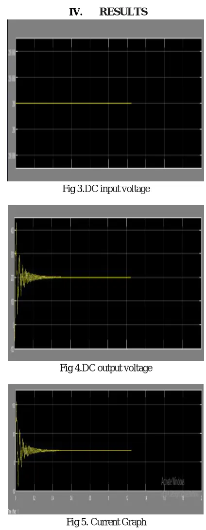
Fig 5. Current Graph
V. CONCLUSION
[image:4.595.189.401.105.650.2] [image:4.595.194.400.121.397.2]REFERENCES
[1] Zambra, D. A. B., Rech, C., &Pinheiro, J. R. (2010). Comparison of Neutral-Point-Clamped, Symmetrical, and Hybrid Asymmetrical Multilevel Inverters. IEEE Transactions on Industrial Electronics, 57(7), 2297–2306.
[2] Qian, W., Peng, F. Z., & Cha, H. (2011). Trans-Z-Source Inverters. IEEE Transactions on Power Electronics, 26(12), 3453–3463.
[3] Trinh, Q.-N., Lee, H.-H., & Chun, T.-W. (2011). A new Z-source inverter topology to improve voltage boost ability. 8th International Conference on Power Electronics - ECCE Asia.
[4] Nguyen, M.-K., Lim, Y.-C., & Kim, Y.-G. (2013). TZ-Source Inverters. IEEE Transactions on Industrial Electronics, 60(12), 5686–5695.
[5] Tang, Y., Zhang, C., & Xie, S. (2007). Z-Source AC-AC Converters Solving Commutation Problem. 2007 IEEE Power Electronics Specialists Conference. [6] Zengin, S., Deveci, F., &Boztepe, M. (2013). Decoupling Capacitor Selection in DCM Flyback PV Microinverters Considering Harmonic Distortion. IEEE
Transactions on Power Electronics, 28(2), 816–825.
[7] Beriber, D., &Talha, A. (2013). MPPT techniques for PV systems. 4th International Conference on Power Engineering, Energy and Electrical Drives.
[8] Das, M., &Agarwal, V. (2014). A novel control strategy for stand-alone solar PV systems with enhanced battery life. 2014 IEEE Applied Power Electronics Conference and Exposition - APEC 2014.
[9] Synchronous Rectification in Quasi-Z-Source Converters: Possibilities and Challenges Liisa Liivik1, Dmitri Vinnikov1,2, Tanel Jalakas1 [10] Enphase S280 Microinverter Datasheet [available online: https://enphase.com].
[11] M. Kasper, D. Bortis, and J.W. Kolar, "Classification and comparative evaluation of PV panel-integrated DC–DC converter Concepts," IEEE Trans. Power Electron., vol. 29, no. 5, pp. 2511-2526, May 2014.
[12] M. Acanski, J. Popovic-Gerber and B. Ferreira, "Design of a flexible very low profile high step-up PV module integrated converter," in Proc. ECCE’2012, Raleigh, NC, 2012, pp. 2942-2948.
[13] B. Gu, J. Dominic, J. S. Lai, C. L. Chen, T. LaBella and B. Chen, "High reliability and efficiency single-phase transformerless inverter for grid- connected photovoltaic systems," IEEE Trans. Power Electron., vol. 28, no. 5, pp. 2235-2245, May 2013.
[14] S. B. Kjaer, J. K. Pedersen and F. Blaabjerg, "A review of single-phase grid-connected inverters for photovoltaic modules," IEEE Trans. Ind. Appl., vol. 41, no. 5, pp. 1292-1306, Sept.-Oct. 2005.
[15] Quan Li, and P. Wolfs, "A review of the single phase photovoltaic module integrated converter topologies with three different DC link configurations," IEEE Trans. Power Electron., vol. 23, no. 3, pp. 1320- 1333, May 2008.
[16] S. Harb, and R.S. Balog, "Reliability of candidate photovoltaic module- integrated-inverter (PV-MII) topologies - a usage model approach," IEEE Trans. Power Electron., vol. 28, no. 6, pp. 3019-3027, June 2013.
[17] S. Kouro, J.I. Leon, D. Vinnikov, and L.G. Franquelo, "Grid-connected photovoltaic systems: an overview of recent research and emerging PV converter technology," IEEE Ind. Electron. Mag., vol. 9, no. 1, pp. 47 61, March 2015.
[18] A. Bidram, A. Davoudi, and R.S. Balog, "Control and circuit techniques to mitigate partial shading effects in photovoltaic arrays," IEEE J. Photovoltaics, vol. 2, no. 4, pp. 532-546, Oct. 2012.