TechniCllI Manual Revision A, August 1981 DISK CONTROLLER 800741/0703/1900
CONTENTS 1. GENERAL
Features
2. PHYSICAL DESCRIPTION Main Disk Controller Auxiliary Disk Controller Disk I/O Cables
Options
3. FUNCTIONAL DESCRIPTION Diskette Storage
1781 Disk Controller Device Addressing
Power On Clear - Reset Timing
Options Read Operation
Write Operation - Single Density Write Operation - Double Density 4. SPECIFICATIONS
6. INSTALLATION Disk I/O Cables Options 5100/5010 Unit
5200 - 5200/5010 Units 6. MAINTENANCE
Customer Support Service 7. REFERENCE
Schematifs and Replaceable Parts Engineering Change Notices OEM Devices
ILLUSTRATIONS
Figure 2:1 - Main Disk Controller - 800741 labia 2-1 - ROM Option Selection
',.iure 2·2 5200 Auxiliary Disk Controller
-MAINTENANCE PAGE 2 2 2 2 4 7 9 9 9 11 11 13 14 15 15 15 15 16 19 19 19 19 19 21 21 21 21 21 21 PAGE 3 4
ILLUSTRATIONS PAGE
Figure 2·3 5010 Unit Auxiliary Disk Controller
-801900 . . . 6 Figure 2-4 - 5100 Disk I/O Cable - 800228 7 Figure 2-5 - 5200 Disk I/O Cable' - 800247 7 Figure 2-6 - System Disk I/O - 800893 7
Figure 2-7 - System Disk I/O - 804475 8 Figure 2-8 - 5010 Unit Disk I/O Cable - 801862 8 Figure 2-9 - 8-lnch Disk 1/0 Cable - 800855 . 8 Figure 2-10 - 5.25-lnch Disk I/O Cable - 800437 8 Figure 3-1 - Main Disk Controller Functional Block Diagram . . . . . . . 10 Table 3-1 - Main Disk Controller S-l00 Bus Signals 12 Table 3-2 - Disk Controller I/O Port 24H and 25H
Functions . . . . . 13 Figure 3-2 - Auxiliary Disk Controller Functiona.1
Block Diagram . _ . . . . . 14 Table 4-1 - Disk Controller 800741/070311900
Specifications 16
•
Figure 5-1 - I/O Cable Signal Paths Between Disk
Controller Elements . . . 18 Figure 71 Main Disk Controller 800741
-Logic:: Diagram
Table 7·1 Main Disk Controller 800741 -Replaceable Parts List
Figure 72 5200 Auxiliary Disk Controller -800703 - Logic Diagram . . . . Table 72 5200 Auxiiiary Disk Controller -800703 - Replaceable Parts List
22
23
26
Figure 1·3 5010 Auxiliary Disk Controller -801900 - logic Diagram . . . . Table 13 5010 Auxiliary Disk Controller -801900 - Replaceable Parts List . . . .
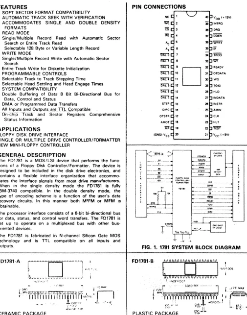
Figure 1-4 - Western Digital FD1181 Floppy Disk Formatter Controller Data Sheet
Table 1-4 - Disk Controller Replaceable Assemblies list . . . . 1. GENERAL
30
31
34
54
1.01 This manual provides a physical and functional description and operating theory for effective field servicing of the dual density 5.25-inch and 8.0-inch Diskette Controller. This manual is applicable to the following:
(1) Main Disk Controller 800741
(2) Auxiliary Disk Controller 800703 (3) Auxiliary Disk Controller 801900 Features
1.02 The Disk Controller is supplied in a two-card set as a system component for Dynabyte 5.25-inch and 8.0-inch diskette storage systems. Features of this Controller include:
• Dynabyte S-100 Bus compatible.
• Single and double-density recording.
• Single density IBM 3740 soft-sector compatible.
• ROM bootstrap.
• Switch-optioned disk I/O port.
• Compatible with 5.25-inch and 8.0-inch media.
• Solder masked pc board.
• Each Disk Controller carries a 30-day warranty on parts and labor.
• Each Disk Controller printed circuit assembly (PCA) is burned in for a minimum of 72 hours.
Page 2
1.03 Dynabyte maintains hardware and software compatability with the Dynabyte S-100 BUf only. The Disk Controller has the followin~ hardware and software requirements:
(l) 2-80 Central Processor Unit (CPU). ThE software for the Disk Controller is writter in Z-80 code.
(2) A 4 MHz clock rate from CPU.
(3) The RAM must operate without wait states
(4) PHANTOM* line must be enabled for RAlV that occupies the memory address spac( from 0 to 256H.
The Disk Controller may not operate with all othe] S-100 Bus computers. Contact Dynabyte fOl
specific applications.
2. PHYSICAL DESCRIPTION
2.01 The Dynabyte Disk Controller for 5.25-inch and 8.0-inch diskettes is implemented as two printed circuit assemblies (peA)s.
Main Disk Controller
2.02 The Main Disk Controller, 800741, is an S-100 Bus card. Refer to Figure 2-1. This PCA measures 5 inches x 10 inches. A 100-pin edge connector mates with the 8-100 Bus connector of the 5100/5200 Computer motherboard. This connector is offset by 5/8 inch from the pc board centerline, i.e., the Main Disk Controller cannot be inserted into a motherboard backwards.
Serial Number Option Strap Option Switch
Table 2-1 - ROM Option Selection Dynabyte
Mnemonic Part Number
803952 RBOOT1A
802033 RBOOT2
802052 RBOOT3
803971 RBOOT4A
804741 RBOQT5
Note:
(1) ID is a single-surface diskette. (2) 2D is a double-surface diskette.
Auxiliary Disk Controller
Dynabyte Equipment
5100 and 5010 Shugart 1D Drives, 5200 and 5010 Shugart 1D Drives, 5200 alone. 5100 and 5010 Remex 1D Drives, 5200 and 5010 Remex 1D Drives, 5200 alone. 5200 and 5010 Remex 2D Drives, 5200 and 5010 Remex 2D Drives, 5200 alone. 5100 and two 5010 2D Drives. 5100 and two 5010 1D Drives.
Two versions of Auxiliary Disk Controllers are available. Each has minor mechanical and electrical differences and measures 6.7 x 5.8 inches. The PCA mounts to the chassis on retainers. Detents secure the PCA in
The Disk
installed in the 5200 ,,'" l ! , . "
to 2-2.
(1) Auxiliary Disk Controller, 800703, has a 34-conductor connector marked MINI DRIVE INTERFACE through which data, status and control signals are exchanged with two 5.25-inch diskette drives.
(2) Auxiliary Disk Controller, 801900, has a 50-conductor connector marked FULL SIZE DRIVE INTERFACE through which data, status and control signals are exchanged with two 8.0-inch drives.
2.06 Distinctive white silkscreened marking has been provided on the component side of the PCA.
(1) The card name, Dynabyte part number and a location for the serial number have been marked on the board. Some early controllers have the serial number etched on the pc board.
(2) Component reference designators are marked where practical. They facilitate locating the individual part on the schematic or replaceable parts list. Refer to Part 7. The Main Disk Controller, integrated circuits and some major components derive their reference designators from the row-column matrix silk-screened onto the pc board. Refer to Figure 2-1. Columns are A to M and Rows are 1 to 3. An integrated circuit located at the lower right corner is M3. The Auxiliary Controller follows a similar convention.
2.07 The Main Disk Controller has two on-board regulators.
UOl +5 Vdc and is provided with an insulated heat sink
U02 +5 Vdc and is provided with an insulated heat sink.
If it becomes necessary to one of these surfaces with a thermal
Figure 2-4 - 5100 Disk I/O Cable - 800228 Disk I/O Cables
2.08 The data, status and control signals are ex-changed between the Main Disk Controller, Auxiliary Disk Controller and diskette drives through flat multi-conductor I/O cablE's. All appear similar. Figures 2-4 through 2-9 illustrate each.
2.09 5100 Disk 1/0 Cable iIIustrated in Figure 2-4 interconnects the Main Disk Controller to the 5100 Computer Unit rear panel. This cable extends the Disk I/O signals up to two external Auxiliary Disk Controllers, e.g., 5010 Units. This cable has 50 conductors and is 21 inches long.
2.10 5200 fJisk 1/0 Cable illustrated in Figure 2·5 interconnects the Main Disk Controller to the 5200 Computer Unit rear panel and Auxiliary Disk Controller in the 5200 chassis. The cable extends the T/O signals to one additional Auxiliary Disk Controller, e.g., a 5010 Unit. This cable has 50 conductors and is 28 inches long.
2.11 System fJisk I/O Cables illustrated in Figures 2·6 and 2-7 interconnect the 5100/5200 Computer Unit with one or two 5010 Units.
(1) System Disk I/O Cable, 800893, is used to interconnect a 5100/5200 and one 5010 Unit. This cable has 50 conductors and is 70 inches long.
Figure 2·6 - System Disk I/O Cable - 800893 (2) System Disk I/O Cable, 804475, is used to
I
Figure 2-7 - System Disk I/O Cable - 804475
Figure 2-8 - 5010 Unit Disk I/O Cable - 801782
2.12 5010 Unit Disk I/O Cable illustrated in
Figure 2-8 interconnects the 5010 Unit rear panel with the Auxiliary Disk Controller in the 5010 Unit chassis. This cable has 50 conductors and is 14 inches long.
Figure 2-9 - 8-lnch Disk I/O Cable - 800855
Auxiliary rh~k Controller
Figure 2-10 - 5.25-lnch Disk I/O Cable - 800437
2.13 8-1nch Disk I/O Cable illustrated in
NOTE
Dynabyte terminates the striped conductor at connector Pin I on I/O cables. Frequently a . (dot) is painted on each
mating conllector to insure correct polarizatioll.
2.14 5.25-lllch Disk I/O Cable illustrated in Figure 2-10 interconnects the Auxiliary Disk Controller with the 5.25-inch drives. This cable has 34 conductors and is 14 inches long.
Options
2.15 The six-position DIP switch on the Main Disk Controller performs two functions: (1) Position 1 ROM Disable - Normally this is closed and enables the Bootstrap ROM located at position K3 on the pc board. (2) Positions 2 through 6 set the decoding
for the upper five I/O port bits. Normally these are factory set to all closed except position 4. This sets the Disk Controller I/O ports to 20H through 25H for Dynabyte Operating Systems. The first four ports are used by the LSI Controller integrated circuit at position MI. The last two ports are used for special control functions on the Main Disk Controller.
2.16 A Disk Clock Strap Option located at Cl sets the clock rate to the Auxiliary Disk Controller.
(1) Position DB8/4 sets the clock rate permanently for S.O-inch drives. (2) Position DB8/2 sets the clock rate
permanently for 5.25-inch drives.
(3) Position DBS/4 8/2 switches the clock rate following the drive select line.
Normally this is factory strapped to the last position.
2.17 The ROM Bootstrap located at K3 contains a firmware subroutine which is phantomed into RAM when a RESET is issued from the
·100/5200 Computer Unit.
3. FUNCTIONAL DESCRIPTION
3.01 The basic function of a Disk Controller is to provide tlw cont.rol elf'dronics necessary for reading and writing data to a diskptt('.
Diskette Storage
3.02 The Disk Control\pr st.ores files and pro-grams on media which is made up of a 0.762 mm (0.003 inch) polyester disk and is enclosed in a matte vinyl jacket. The entire assembly is called a diskette or colloquially, a floppy disk. The polyester disk substrate is coated on both sides with 2.541Jm (100 microinch) ferrous oxide similar to that found on audio tape. Thp diskette is fl(>idble and is intended to deform slightly as the revolving disk is pressed onto the surface on the read/write head in the disk drive.
3.03 The Operating System dividps the available read/write area on the disket.t.e into tracks or concentric circles. Individual tracks are further subdivided into sectors.
(1) 5.25-inch diskettes are organized into 77 tracks numbered OOH t.o 4CB. Each track has 32 double-density (OD) sectors.
(2) S.O-inch diskettes are also organized into 77 tracks numbered OOH to 4CH. Each track has 26 single-density (SD) or 54 double-density (DD) sectors.
Information may be stored on one surface (1 D) or both surfaces (2D) of a diskette. 20 storage requires driv(Os with two read/write heads. The tot.al storage capacities for 10 and 2D operation are tabulated in Part 4.
3.04 The disk formatting operation prerecords track and sector information onto the disk. The sector locations are determined logically or soft sectored. A single index hole in the disk is monitored by the disk drive electronics. An INDEX pulse is furnished to the Auxiliary Disk Controller each .time the disk st.arts a new revolution. The diskette can then he accessed random Iy by the Disk Controller for read/write operations.
,OUT
-4 MHZ PHASE 2
pSYNC
HLD
Wait State
1
Generator ORa INSTR
.nd
i
Status Ports
INTR
HLD
t Oisk INQATA·
t
ControllerOTDATA·
1781
RESET* elK
, MR'
POC'
DAl' tiLT
:
•
!
r
l
i
8
:
(2
f
I
t-$
I I
l'
I
,
,
000
7
010 7 j : i I-
I
16t t I
I
:
J
,I
iAO ~16 I
Buffet"
:
,
:j
I!
i
,
/ 8) Status and Control
Buff~ :
!
,I
j
1
(
1
+
12
6
i i
sMEMR 0
I
,
'*
j. II
2
ROM
Port Bootstrap
88it 3
Addrns
"'"
Decode MemOrt Latch
Phantom 4
5
•
6p08!N ,
i
71
I
ROM Enable
i
I
i
ROM Oisable [image:10.814.72.726.52.499.2]I
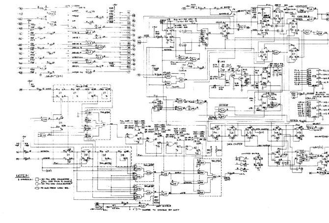
Figure 3·' - Main Disk Controller Functional Block Diagram
ROY
Read Enable
and XROY
Input Strobe GeneratOf'
CLEAR
i
L:fJ
INOATA OTDATA WRCLK~ elK HLT HlD MUltiplexer Clock Selector
Doubte Oemity and
I~
Head loadDelav
i CLOCK--IIi
I
iII
I
0.0· 0.15I
I
812
~.J,
D,'v. Clock 16I
8/4 Option Strap! 8/2· 8/4 L--..o ~
STATUS AND CONTROL
I
i !I
i i
1
i
1
SIDE SELECT O·
DRIVE 1~
DRIVE 2·
DRIVE 3'
DRIVE
4-DOUBLE DENSITY
AUX BOARDO'
PHANTOM·
1781 Disk Controller Device
3.06 The principle element of the Disk Control-ler 800741/0703/1900 is a 1781 Disk
Controller large scale integrated (LSI) circuit.
Part 7 provides the technical data sheet on this OEM device. The sheet furnishes detailed functional descriptions on:
(1) Organization of the registers, CRC Logic, ALU and Timing/Control.
(2) Processor Interface.
(3) Diskette Interface.
(4) Head Positioning, Disk Read Operation.
(5 ) Disk Write Operation.
(6)
Command Description and Flow Charts.(7) Formatting the Disk. (8) IBM 3740 Format.
(9) Non-IBM Formats.
_ .lis manual will confine its functional descriptions to the Main and Auxiliary Controller elements.
3.07 The main data transfer function performed by the 1781 Disk Controller is to convert 8-bit parallel DAL* to serial OTDATA on write operations and serial INDA T A to 8-bit parallel DAL* on read operations. Figure 7-4 details the function of each device line. Figure 3-1 summarizes and illustrates the most significant of these lines. Drive control lines have been omitted.
(1) Master Reset (MR*) is a logic low from RESET* or POC* and resets the 1781
Disk Controller clearing the command register.
The Not Ready, Status Bit 7, is reset when MR * is active.
(2) Data Acqess Lines (DAL*) is an eight bit inverted· bi-directional bus used for transfer of data, control and status.
(3) Data Request (DRQ) performs two func-tions. It indicates the data register contains assembled data in read operations or the register is empty in write operations. The DRQ is reset when the CPU reads or loads the register.
(4) Input Strobe (INSTR) indicates INDATA is valid.
(5) Input Data (lNDAT A) is the date line from drive and is valid when INSTR is active.
(6) Output Data (OTDATA) is the date line to drive and is valid when OTSTR is active. (7) Head Load (HLD) output controls the loading of the Read-Write Head against the media. The HLT input is sampled every 10 ns. When a logic high is detected on the BLT input, the head is assumed to be engaged.
(8) Head Load Timing (HLT) signal is generated bya ltmltivibra.tor in the H eadL oaillJelay
since the drive does not furnish this signal when the media is engaged.
(9) Clock (CLK) is the internal time reference for the 1781 Disk Controller.
Addressing
3.08 Data transfers are performed by programmed I/O. Five of the O,1Iion Switch
positions set tl~e Disk Controller address for the
Port Address I>ecode. Dynabyte Disk Operating
Systems use Ports 20H through 25H for the Disk Controller.
(1) Ports 20Hto 23H are used by the 1781 Disk
Controller for I/O operations. These
correspond to the 1781 I/O Ports 0 - 3 and their functions are described in Figure 7-4 under Processor Interface.
(2) Ports 24B and 25H are used by the other elements of the Disk Controller. Their functions are tabulated in Table 3-2.
Writing to Ports 24H and 25H set the individual
8-Bit Latch functions.
(3) Side 0 SELECT* determines the surface accessed on 2D drives.
(4) DRIVE 1 through 4* determines the drive to be accessed. An Auxiliary Disk Controller is designed to support up to four drives. Dynabyte systems currently use only two drives per Auxiliary Disk Controller.
Name
4 MHZ PHASE 2 A l - A15
CLOCK
DIO - DI7 DOl- D07
PHANTOM *
POC*
RESET*
XRDY
pDBIN
pSYNC
pWR*
RDY
sINP
sMEMR
sOUT
Table 3·1 - Main Disk Controller S·100 Bus Signals
Pin
24
Various
49
Various
Various 67
99
75
3
78
76
77
72
46
47
45
Function
The master timing signal for the bus.
Address Bit 1 through Address Bit 15.
2 MHz (0.5%) 40% - 60% duty cycle. Not required to be synchronous with any other bus signal.
Data In Bit 0 through Data In Bit 7.
Data Out Bit 0 through Data Out Bit 7.
A bus signal which disables memory during Disk Controller ROM access.
The Master Reset Signal. The Power On Clear signal for all devices. When this signal is low, it must stay low for at least 10 ms.
Requests the reset of all bus master devices. Connects to the Front Panel Reset Switch and activates POC*.
One of two ready inputs to the current bus master. The bus is ready when both these ready inputs are true. Sin Pin 72.
The control signal that requests data on the DI bus.
The control signal identifying the beginning of a processor cycle.
The control signal signifying the presence of valid data on the DO bus.
See comment for Pin 3.
The status signal identifying the data transfer bus cycle from an input device.
The status signal identifying bus cycles which transfer data from memory to a bus master, which are not interrupt acknowledge instruction fetch cycle(s).
Table 3·2 - Disk Controller I/O Port 24H and 25H Function
Port Name Bit Function
24H
STATUS
HEAD LOAD 0 Indicates head is loaded.
1-3 Not defined.
INTRQ* 4 Indicates operation is complete.
5--B Not defined.
INTRQ* or 7 If this bit is active, the status of Bit 4 is read to determine if an
TIME OUT* operation is complete or timed out.
CONTROL
SIDE 0 SELECT* 0 Selects side (surface) O.
DRIVE 1
*
1 Selects Drive l.DRIVE 2* 2 Selects Drive 2.
DRIVE 3* 3 Not Defined.
DRIVE 4* 4 Not Defined.
DOUBLE DENSITY* 5 Selects double density recording. AUX BOARD 0* 6 Selects Auxiliary Disk Controller O.
ROM ENABLE 7 Enables ROM Bootstrap.
25H Status and control functions an' similar to 24H except a wait
state is generated.
(6) AUX BOARD 0* determines thp Auxiliary Disk Controller addresspd.
and the 1781 Oisk COlllroller through MR*. A similar function is performed when the operator keys the front panel RESET pushbutton. The R
o
!IfBoolstrap is ov('rlaid into RAM starting at location
OOH when the PHANTOM* line goes low. While thf' PHANTOM* is activated, all memory reads are from the ROM Bootstrap. An active Pf-fANTOM* lilw does not inhibit writing t.o RAM however. (7) ROM EN ABLE provides for enahling the
ROM Bootstrap phantoming operation during power on or reset. Refpr to 3.09.
Reading from 24H and 25H furnished drive status. e.g., head loading.
Power On Clear - Reset
Each time the computer is powered on, the POC* line goes low clearing thE' CPU
(1) The CPU reads the inst.ruct.ions starting at addrpss OOH. These instructions direct t.he CPU to read Track 0, Sector 1, from Drive A.
This particular o~wratiol1 is called the ROM
(2) Track 0, Sector 1, is read. This sector contains additional instructions which are loaded into RAM for execution. This operation is called the Disk Bootstrap.
(3) The first two tracks, 0 and 1, contain the Operating System and are loaded from the top of RAM down.
(4) The CPU disables the ROM Bootstrap by setting Bit 7 of the 8-8i1 Latch.
(5) The PHANTOM * line goes high.
The ROM Bootstrap may also be optionally
disabled by an option switch for special applications.
Timing
3.10 The Wail State GeneratOf: creates wait states by holding RDY or, optionally, XRDY lines low to the CPU. This element is necessary since the CPU can operate significantly faster than the
1781 Disk Controller. Wait states are generated:
(1) During all [/0 instructions to the 1 781 Disk COlltroller.
-
7 I(2) During data transfer operations to insure synchronization.
Three Disk Controller timing functions are performed by the Multiplexer Clock Selector And /lead Load Delay.
(3) Head Load Delay is performed by a multi-vihrator activated by HLD, the Head Load command. The multivibrator furnished HLT to
the 1781 Disk Controller after a period set to
the drive head load time specifications. This is necessary since the drive does not furnish HLT when the head is in contact with the disk. (4) The S-100 Bus CLOCK is counted down
to generate WRCLK* the Write Clock, furnished to the drive.
(5) In addition S-100 Bus CLOCK is counted down to generate CLK to the 1781 Disk Controller .
The AUX BOARD 0* line causes the multivibrator timing to change and both clock rates to change between 5.25-inch and 8.0-inch Disk Clock rates when the DB 8{2 8/4 Option Strap is in place. Refer to 3.13.
"'
Statui. Control ,nd Orive $elKt •CLEAR OTSTR SO" Write Data 00 = Output Data Strobe
INDATA
I
OTDATA ~
WRClK' AMOT Oouble Sol ...
Density Single
--_
.. _- WrittDtltl ..AO AI5 ~A _ _ _ - - - . O.ta 0<
-... Encoder Double
STATUS AND CONTROL TO 43 Enable
. so Ohm Line
SIDE SELECT O'
.---.
Recetversi end
i
DRIVE I' Ttlnsmiu"rtu DRIVE 2' AMIN
~ DRIVE 3' Rud 0. ..
~ c
~ DRIVE 4' CIta,
...
Read O.r.
DOUBLE DENSITY -
...
Oat. Window Oat,. SeparatorWrite Clock
Enable ~,Denslty
T
AUX BOAROO·
~.~
[image:14.641.38.570.353.704.2]' - -
t.
0 'Options
3.11 The Disk Clock Strap Options on the
MIl/tiIJ/exer Clock Separator provide for
the following:
(1) DB 812 sets the WRCLK* and CLK to the 5.25-inch diskette data rate. This is appropriate for a 5200 Computer Unit without a 5100 Unit connected.
(2) DB 8/4 sets the WRCLK* and CLK to the 8.0-inch diskette data rate. This is appro-priate for a 5100 Computer Unit and one or two 5010 Units.
(3) DB 8/2 8/4 causes the WRCLK*' and CLK to toggle between the 5.25-inch and 8.0-inch diskette data rates depending on which drive is selected. This is appropriate for a 5200 Computer Unit and 5010 Unit.
The Bootstrap ROM, discussed in 3.09, provides
the Operating System with hardware system options for the particular system. For example:
(4) Number of disk drives,
(5) The sizes of the disk drives,
(6) Number of surfaces per disk drive.
The A IIX Select Option strap determines whether
the Auxiliary Disk Controller will be 0 or 1 in the disk storage system.
(7) The 5200 Auxiliary Disk Controller is normally strapped as O. If a 5010 Unit is used in conjunction with a 5200 Computer Unit, the 5010 Auxiliary Disk Controller is strapped as 1.
(8) The first 5010 Auxiliary Disk Controller connected to a 5100 Computer Unit is strapped as 1 and the second 5010 Auxiliary Disk Controller is strapped as O.
Read Operation
3.12 The Head Loaded, HLD, and a Data Request, DRQ, cause Read Ellahle and
Input Strobe Generator to set CLEAR low initiating
a read operation between the Auxiliary Disk ('nntroller and the drive selected. When CLEA R iligh, the Auxiliary Disk Controller is in a
passive mode and is not attempting to acquirp data. It may be:
(1) Writing data to a drive, or (2) Waiting to be accessed.
The Phase Lock Loop (PLL) within the Data
Separator is locked on to the Write Clock while
CLEAR is high. During a read operation, CLEAR is low. The PLL is locked to the drive Read Data Synchronization Field.
(3) When the Data Separator detects an address mark, AMIN is strobed high. The 1781
Disk Controller acknowledges AMIN by holding
CLEAR low. If an address field is not detected in a predetermined time interval, the CLEAR is spt high.
(4) Data Window is the strobe indicating a data field is prpsent.
(5) Read Data is output to the 1781 Disk
Controller as OTDAT A for transfpr to the
CPU and RAM.
Write Operation - Single Density
3.13 In single density (SD) operation. the 1781
Disk COfltroller encodes write data and
outputs it to the Auxiliary Disk Controller. Also, in SD operation the OTSTR, Output Strobe, is Write Data which is gated through ,\"e/ect Single
or Douhle without further processing.
Write. Operation - Double Density
3.14 In double density (DD) operation, the
1781 Disk Controller does not perform
any encoding. OTDATA is write data in NRZ format strobed to WRCLK*.
(1) DOUBLE DENSITY line selects double in the Selec/ Single or Douhle.
(2) AMOT high indicates Address Mark Out enabling Write Data to drive.
(3) OTDATA is encoded into double density MFM and strobed as Write Data to the drive by OTSTR.
4. SPECIFICATIONS affect the Computer System operation are excluded from the Dynabyte, Inc., warranty.
4.01 Table 4-1 summarizes the Disk Controller 800741/0703/1900 functional and physical performance specifications as a system unit. Minor deviations from these specifications which do not
4.02 Figure 7-3 includes the functional and physical performance specifications for the OEM Disk Controller integrated circuit.
Table 4-1 - Disk Controller 800741/0703/1900 Specifications
PARAMETER CHARACTER ISTIC
Main Disk Controller
Controllerpevice Western DigitalFD17.81
_.
I/O Ports 20H through 25H
Mode SD or DD
Capacity Two Auxiliary Disk Controllers
Auxiliary Disk Controller
Capacity Two 10/2D 5.25-inch or 8.0-inch drives
Format, SO IBM 3470
,DD Dynabyte Double Density
5.25-inch Media Soft sectored
Heads,1D 1
,2D 2
Tracks Per Surface 77
Media, 10 Dysan PIN 800439
,2D Dysan PIN 802067
Unformatted Capacity
Surface, DD 480K Bytes
Formatted Capacity
Sector Size, DD 128 Bytes
Sectors Per Track, OD 32
Surface, DO 315K Bytes
Transfer Rate, DD 250K Bytes per second
Encoding Method, DD MFM
8-inch Media Soft Sectored
Heads, 10 1
,2D 2
Tracks Per Surface 77
Media,1D Dysan PIN 800528
,2D Dysan PIN 800803
Unformatted Capacity
Per Track, SD 5,212 Bytes
,DD 10,425 Bytes
Formatted Capacity
Sector Size, SO 128 Bytes
,DO 128 Bytes
Sectors Per Track, SD 26
Table 4·1 - Disk Controller 800741/0703/1900 Specifications (Continued)
PARAMETER CHARACTERISTIC
8-inch Media
Formatted Capacity
Surface, SD 256K Bytes
,DD 525K Bytes
Transfer Rate, SD 250K Bytes per second
DD 500K Bytes per second
Encoding Method, SD FM
,DD MFM
Main Disk Controller Power Requirements
+16 Volt Bus Regulated to +12 V de
+8 Volt Bus Regulated to +5 V de
-16 Volt Bus Regulated to -12 Vdc
Operating Temperature 10°C to 35°C (50° F to 95° F)
Dimension, Width 24.5 cm (10.0 inches)
, Depth 1.5 cm (0.6 inches)
, Height 12.7 cm (5.0 inches)
, Weight 215.5 g (7.6 ounces)
Auxiliary Disk Controller Power Requirement
+5 Vdc Supplied from chassis power supply.
Operating Temperature 100C to 35°C (50°F to 95°F)
Relative Humidity 20% to SO%
Dimension, Width 17.0 cm (6.7 inches)
, Depth 14.7 cm (5.S inches)
, Height 2.0 cm (0.8 inches)
, Weight 109.S g (7.4 ounces)
Note:
404070
800288 Cable: Disk 1/0
800741 PCA: Main Disk Controller
800247 Cable: Disk 1/0
50
800741 peA: Main Disk Controller
800703 peA: AUM'i'iary Disk Controller
5010 Rear Panel
I
801782 Cable' Disk 110~(~1~---~7/~50---<
1 801900 PCA: Auxiliary Disk Controller
5100R_Pmol
1
I )
5200 Rear Panel
800437 Cable: S.2S·lnch Disk 1/0
DU81 S.2S·lnch Diskette
Drives
800855 Cable: 8·lnch Disk 1/0
Qual8·1nch
Oi'Skettf!
[image:18.635.40.548.65.714.2]Drives
5. INSTALLATION
11 Refer to 5100/5200 Computer Unit Technical Manual for unpacking, inspection and return of material procedures. The Disk Controller is normally supplied as part of a Dynabyte Storage System. The following proce-dures are appropriate when replacing a Controller PC Assembly or I/O cable and will serve as a check list for installation.
Disk I/O Cables
5.02 Figure 5-1 illustrates the I/O Cable signal paths between Disk Controller elements. Part 2 illustrates each of these cables. A computer unit is connected to one or two Disk Storage Units with aSystem Disk I/O Cable. .
NOTE
Always check to make certain the peA options agree with the individual system equipment configuration before turning on the Dynabyte
computer system.
ions
5.03 The basic controller design provides for various computer storage configurations through ROM, Switch and Strap Options on the Controller PC Assemblies.
5100/5010 Units
5.04 The following procedure will serve as an option check list when a 5100 Computer Unit and one or two 5010 Storage Units are used together or a single 5010 Unit is expanded to two 5010 Units.
STEP PROCEDURE
1 For a 5010 Unit installation, check the Main Disk PC Assembly options:
(1) Disk Clock Strap Option to DB8/4 8/2 position,
(2) A ROM should be installed
I
STEP PROCEDURE
appropriate to drive manu-facturer and number of surfaces. Refer to Figure 2-1 for the loca-tions of these oploca-tions.
2 Check the Auxiliary Disk Controller PC Assem bly options for a single 5010 Unit installation:
3
4
(1) Address Strap to 1,
(2) Terminating resistor pack in-stalled at A3.
For a two 5010 Unit installation, check the Main Disk Controller PC Assembly options:
(1) Disk Clock strap option to DB8/4 position,
(2) A ROM should be installed appropriate to drive manu-facturer and number of surfaces. Refer to Figure 2-3 for the loca-tion of these oploca-tions.
Check the Auxiliary Disk Controller PC Assembly options for a two 5010 Unit installation:
(1 ) Unit 1 Address Strap to 0, (2) Unit 2 Address Strap to 1,
(3) Unit 1 A3 vacant,
(4) Unit 2 terminating resistor pack at A3.
Refer to Figure 2-3 for the locations of these options.
5200 - 5200/5010 Units
NOTE
Only one Terminating Resistor Pack should be installed in a Disk Storage System. The Resistor Pack should only be installed in the last Auxiliary Controller in the Disk
Storage System.
STEP PROCEDURE
1 For a stand-alone 5200 Computer Unit installation, check the Main Disk Controller PC Assembly options:
(1) Disk Clock Strap Options to DB8/48/2 position.
(2) A ROM should be installed appropriate to drive manu-facture and number of surfaces. Refer to Figure 2-1.
2 If the systetn does not include a 5010 Unit, check the Auxiliary Disk Con-troller options in the 5200 Computer Unit:
(1) Address Strap Option to 0, (2) Terminating Resistor Pack at
A3.
3 If the system does include a 5010 Unit, check the Auxiliary Disk Controller PC Assembly options in the 5010 Unit: (1) Address Strap Option to 1, (2) Terminating Resistor Pack at
A3.
5.06 The Main Disk Controller can be installed in any of the 12 card cage positions. As a matter of cabling convenience, it should he installed as shown in Figure 2-3 of the 5100/5200 Computer Unit Technical Manual.
STEP
1
2
. PROCEDURE
Install the Main Disk Controller into the card cage.
NOTE
The 50-conductor I/O cables are polarized with a stripe on
conductor I.
6. MAINTENANCE
i)1 The Disk Controller 800741/0703/1900 is a result of several years of design, develop-ment and modern electronic manufacturing. The pc assembly is designed around the latest semi-conductors and integrated circuits. All components operate at relatively low power. Each assembly is burned in at the Dynabyte factory for 71 hours before shipment. It can be expected to operate indefinitely.
6.02 No routine maintenance should be per-formed to the Main or Auxiliary Disk Controllers.
Customer Support Service
6.03 Maintenance and procedures described in this manual should be performed in accor-dance with local instructions and the individual user's maintenance plan. Maintenance and repair of the Disk Controller during the warranty period should be limited to returning the pc assembly to Dynabyte, Inc. The Dynabyte Customer Support staff is available by telephone for assistance in troubleshooting and recommendations for repairs. ( . -, communications and material should be
'L _ dcted to:
DYNABYTE, INC. Customer Support 521 Cottonwood Drive
Milpitas, CA. 95035 (408) 263-1221
Telex 346-359
The 5100/5200 Technical Manual, Part 6, outlines the procedure for returning material.
NOTE
Dynobyte Authorized Service Centers (ASC) are staffed with factory-trained technicians that are supplied with technical manuals and routinely receive service bulletins and design change information on Dynabyte equipment.
7. REFERENCE
Schematics and Replaceable Parts Lists
7.01 Figures 7-1, 7-2 and 7-3 will furnish the user with schematic diagrams of th~ Main and Auxiliary Disk Controller. Tables 7-1, 7-2 and 7-3 are replaceable parts lists of Main and Auxiliary Disk Controller pc assemblies indexed by reference designator appearing on the respective schematic. Enough information is furnished so the maintenance technician should be able to purchase replaceable parts from a local supplier or make a substitution if necessary. Disk Controller PC Assemblies, ROMs and 1/0 cables should be ordered directly from Dynabyte Customer Support ServICe.
Engineering Change Notices
7.02 Dynabyte makes changes to drawings and products through engineering change notices (ECN)s. Before a change to a product is approved or made:
(1) The implications to systems in the field are determined,
(2) Rework instructions are included for the equipment in the field when appropriate. Dynabyte Customer Support Services receives copies of all ECNs and advises Dynabyte Authorized Service Centers through seminars and periodic bulletins.
7.03 There are no pertinent ECNs affecting the Disk Controller at the publication date.
OEM Devices
L -________ ~~~--~--v~~~~--~~
k -_ _ _ _ _ _ ~~~--~~~~
L -_ _ _ _ _ _ _ _ ~~
P.U. =tSV
A_& DB8,,4
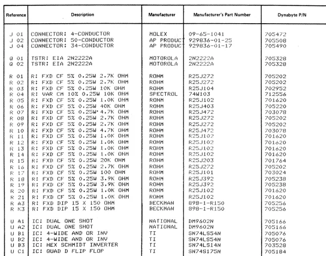
Reference Description Manufacturer Manufacturer's Part N!Jmber Dynabyte PIN ,
PCf-) : MAIN II I !;,< CDNTR(}L.L.EF~ DYNABYTE
iJ0074:t
800741 C(.)BI...E: ~:51 00 DISI< I/O DYNf.)IWTE 800228 800228
C(.H~f...E t ~)200 DISK I/O DYNABYTE 800247 800247
C OJ. C! FXD TANT 10% 35V :I..OUF SPI~AGUE :1. 96D:I. 0::)X9(B~:)H(.u 711~);:W
C O:::.~ ("' .,
.
.
FXD TANT :LO% 3~)v O.47UF SPRfiGUE :L50D 7068::=jiJC 03
c:
FXD T(.)NT :lOY. 6V 6BUF SPRAGUE 196D6iJ6X9006KAl 706840C 04
c:
FXD CER lO% :LKV 100PF CENTRALAB DD:lO:I. 70;3978C 05 C+ FXD rANT I •
:toY.
~~5V :I.OUF SPI~AGUE :L 9tlD:l 06X90251<Al 707254C 06 C+ FXD TANT :LO% 25V :LOUF SPRAGUE :I.
9!!i1):I. 06X902~)KAl 707254 "
C
O?
f~ ~. • FXD rANT:toy.
251,.1 :l.OUF SPI:;;AGUE :I. 961H 06X902:3KAl 707254 C :1.0c·
~..
FXD CER 20% 12V .. llJF CENTI=\:AI...AB UK 12·· .. 1. 04 703294C 11 (~
:
FXI) CER 20% :L2V • :I.UF CENTRALAB UK 12'-l 04703294 C :l ::~
C!
FXD CER 20% L~V .. :I.UF CENT/=i:r=iL.AB U/<1.2·-:L04 703294 C 13c:
FXD CEI:;;2()Y.
12V • HJF CENHi:A/ ... AB UK12-104 703294C 14
c·
FXD CER 2()% 12V .:LUF CENTR(.)LAB UK 1 2·- 1 04703294 .'
.
c:
1 ~:ic:
F:xD CER 20% 12V • lUF CENll:<r:)L.AB UK 1 2,-1 04 703294C 16
c:
F.:<D CER 20% 1.2V • :I.UF CENTR(.~L.AB UI<12·-:L04 703294 C 17 C., .,.
F~-<D CER 20~' 121,.1 .J.UF CENTRr:)/...f.1B I..IK12-·J.04703294 C 18 ('. I •
FX[I
eEl::; ::~~o i~ 12V .1UF CENTF:f:)/",f.1B UK 1 2·-104703294
C 19
c·
'.
FXD
CEI~ 20% 12V .lUF CENTF~A/"'AB UK12··-104 703294C 2()
c:
Fx:D CER 20:r. 12V .:J.UF CENTI::;(:)I...AB UK:L2 .... :l.04703294 C 2:1.
c"
.,.
FXD
CE:R ;.~O;{.12V
.1UF CENTF:I:)L.':~IB UK 12 .... :1. 04 703294 C '.'} 1").\
...
~.c.
FXD CER ;~O% L2V .1UF CENTI~:AL.i~B UI<12· .. ·:/.()4703294 C ~::3 C· '
.
F)(D CEf~ 20% 12V • .I. UF CENTr;:tl/"'(iB UI< :1. ::2·_·1. 04' 70;3294C 24
c:
FXD
CER 20%:L2V
• :l UF CENTRAI...AB UK:l.2 .... :L04 703294 C ''')':' C·FXD CER ;.~O% L~V .HJF CENTf<tlLAB UI<:l.2·"·104 703294
.... J I •
C 26 C+ FXD CER 2()% .,
.
:t2V
.1UF CENTI:<AL(:IEI UI\ 1 2·- 1 04 703294CR () DIODE! EIA :I.N96:~ MOTOROLf)
l.N963 704770
F' 01 CONNECTOI::; : ~50-CONDUCT[)f~ f)P PRODUC' 9298:m"-()1 -2~) 7032()4
r~ 0:1. R: FXD CF 5:Y. O. :~:)W 2701< OHM ROHM f\2~U274 701728
R 02 R: FXD CF 5:Y. O.25W 2001< OHM ROHM 1~25.J204 711620
f~ 03 R! VAr.:: CM 1. ()% O.25W. 201< OHM SPECnWL. 6~5S2()~5 7047:~4
[image:23.791.63.714.50.556.2]Reference Description Manufacturer Manufacturer's Part Number Dynabyte PIN
I;:
06
r' •
'\.
FXD CF
~)/.0.2!'5(..1
2701';OHM
ROHM
1:;:25J274701728
R 07
R: F-XD CF
5%0.5W 200 OHM
ROHM
R50J201
704680
R 08
R: FXD CF
5%O. 2~5W
10K OHM
ROHM
R25,J104
702952
R
09
R: FXD CF
5%0.2!5W 10/< OHM
RCJHM
R2!:),J1 04
702952
H
10
R: FXD CF 5% 0.25W
:l.0/< OHM
ROHM
I:;:25,.J 1 02
701620
f~ 11
R: FXD SIP 7 X 1!50 OHM
BECKMAN
785--1-R:L !:iO
704698
H1 --:)
-~-R: FXD
~;rp7 X 4.7K OHM
BECKMAN
764-1-4--4 • .7K
704716
5 01
SWITCH: 6-PO!3I T I DN SPST DIP
GRAYHIl.l.
765B06
704824
U
01
IC: REGUU'HOR +5V
TI
7805C
703168
U
02
IC: REGUl.ATOR +5V
TI
7805C
703168
U
Al
IC: HEX SCHMIDT INVERTER
n:
SN74l.S14N
703528
U
A2
Ie:
DUAL MULTI VIBRATOR
TI
SN74L.S:l.23N
704878
U
A3
IC: (WA[i 2-IN NAND DC
TI
SN7438N
705346
U
Bi
Ie:
DUAL MULTIVIBRATOR
TI
SN74LSi23N
704878
U B-'" .:..
IC: UP/DOWN COUNTER
TI
SNl.S193N
704932
U
B3
IC: (WAD 2-IN AND
TI
SN740BN
704860
U
C1
IC: QUAD 2-IN NAND SCHMIDTT
TI
SN74U;132N
703582
u
C2
IC: QUAD 2-TO l-l.INE MUX
TI
SN741_!:,j7N704914
U
C3
IC: DUAL D FLIP FLOP
TI
SN74L.S74N
704050
U
D2
Ie: (WAD 2-TO 1--LINE MUX
TI
SN74157N
704914
U D:3
IC: UP/DOWN COUNTER
TI
SNl.S193N
704932
U
E1
IC: QUAD 2-IN
(m
TI
SN7432N
703546
U E2
IC: QUAD 2-IN NOR
TI
SN7402N
703456
U
E3
IC: UP/DOWN COUNTER
TI
SNLS193N
704932
U F1
IC: QUAD 2-IN NAND OC
TI
SN7438N
705346
U F2
IC: HEX BUFFER
TI
SN74LS367N
707200
U
F3
IC: HEX SCHMIDT INVERTER
TI
SN74LS14N
703528
U
H1
IC: QUAD 2-IN NAND OC
TI
SN7438N
705346
U H3
IC: HEX BUFFER
SIGNETICS
N8T97N
704968
U
J1
IC: QUAD 2-IN NAND OC
TI
SN7438N
705346
U J2
IC: 6-BIT COMPARATOR
NATIONAL
DM8131N
705004
U J3
IC: HEX BUFFER
SIGNETICS
N8T97N704968
U
Kl
IC: HEX SCHMIDT INVERTEf<
TI
SN74LS14N
703528
U
K2
IC: QUAD 2-IN AND
TI
SN7408N
704860
-Reference . Description Manufacturer Manufacturer's Part Number Dynabyte PIN
U
K3
Ie:
RBOOT5 READ ONLY MEMORY
DYNABYTE
804741
804741
U
K3
IC: RBOOT1A READ ONLY MEMORY
rlYNABYTE
803952
803952
U
K3
IC: RBOOT2 READ ONLY MEMORY
DYNABYTE
802033
802033
U K3
IC: RBOOT3 READ ONL.Y MEMORY
DYNABYTE
802052
802052
U
Ll
Ie:
(WAD 2-1N NAND
DC
TI
SN7438N
705346
U
L2
IC: OCTAL
DLATCH
TI
SN74LS273N
704950
U
L3
Ie: 5-BIT SHIFT REGISTER
TI
SN74LS96N
703726
U
Mi
IC: DISK CONTROLLER
WESTERN
D.FD1781-B
704986
Reference Description Manufacturer Manufacturer's Part Number Dynabyte PIN
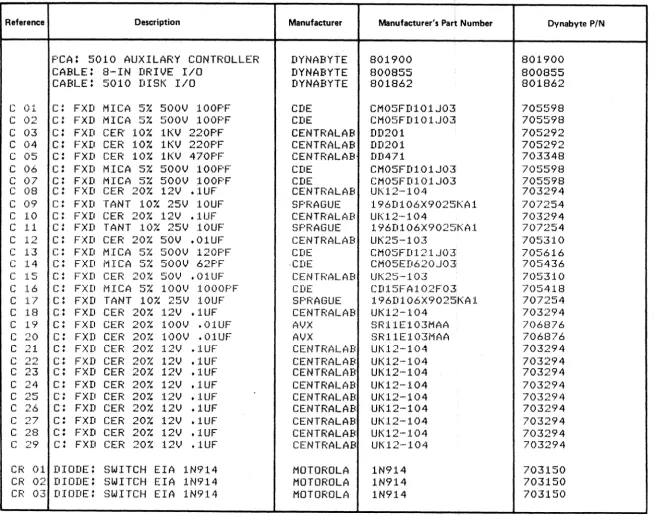
peA: 5200
ALJXILAF~YCONTROLL.ER
DYNABYTE
800703
800703
CABL.E: 5.25-IN DFUVE I/O
DYNABYTE
800437
800437
C
01.c·
..
FXD MICA 5/.
~)()OV240PF
CDE
CM05FD241.J03
705400
C02
C+....
FXD MICA 5/.
~iOOV240PF
CDE
CMO!5FD241.J03
705400
C 03C·
'.
FXD CER
10/.l.KV 220PF
CENTRALAB
DD:Wl
705292
C 04
C·
..
FXD CER
lOr.
:LKV 220PF
CENTRALAB
[1[1201
705292
C O~)C: FXD CER :LOr. J.!-'V 470PF
CENTRALAB
D[l471
70:3348
C 06
C+....
FXD MICA
~):Y.500V 240F'F
CDE
CM05FD24:L.J03
705400
e:
07c·
'.
FXD MICA
~5Z ~'iOOV240F'F
CDE
CM05FD241 ~J03
7054()0
C 08
C: FXD CER
20r.
12V .1UF
CENTR(~LABUI-( 12·- 1. 04
703294
C 09
C·
....
FXD
TI~NT:LOr. 25V
lour
SPRAGUE
196Dl06X9025KAl
707254
C
10C: FXD
CEF<20r.
12V
• :1. UFOCENTRAL.AB
LJI-( 12,-1. 04
703294
C
11 c; !FXD TANT
lOr.
2!:'jV
lour
SPRAGUE
1.96D:L06X9025KA1.
707254
C 1.2
C: FXD CEr..: 20;{. !5()V .OHJF
CENTRAL.AB
UK25···1 ()3
705310
C
1,3
C·
,.
FXD MICA
~:)% !:,j()()V 240PF
CDE
CM05FD241.J()3
70!5400
C
14
C·
.,.
FXD M.I
CI~ ~5;('::'iOOV 1.20F'F
CDE
CMO!:'jFD:J.:21,.103
705616
C
1.:'5c·
, +
FXD CEI:;:
:~O/~ ~50V.O:U.JF
CENTRI~LAB I.JK:?~:)·-:I.0:3
705310
C If.>
C·
,.
FXD MICA
C:-"I.... ·l.
1001,,1 10OOF'F
CDE
CD1~5FA102F03705418
e
1 '7 IC·
,.
FXD TANT lOr. 25V
:tOUFSPRfiGUE
1.96Dl06X9025KAl
707254
C 1.8c+
....
FXD CER 20:>.:
L~V• HJ F
CENTRAL.AB
LJKL2-·104
703294
C
1.9C: FXD CER
:I. o;{.!5()V •
02~~UFAVX
SR265C223KAA
705382
C 20 C!
FXD MICA
~)%lOOV :lOOOPF
CDE
CD15FA:l02F03
705418
C
21
(:
:
FXD CER 20% :l.2V
• :I.UFCENTRALAB
UK1.2·-104
703294
t
") "J ...:..
c·
,.
FXD CER 20% :l.2V .:LUF
CENTFMI...AB
UK:l.2·-104
703294
C
23
C: FXD CER
20~~12V .:l.LJF
CENTRALAB
UK:I.2-104
703294
C24
c:
FXD CER
2()r.
12V
• :tUF CENTF~ALABUI\:L2-104
703294
c;
1"") I:".~J
C: FXD CER 2()% 12V .:lUF
CENTRALAB
LJI-(12"·104
703294
C
26
{: !FXD CER
20r.
:L2V
.1UF
CENTR(~LABUK 12··'
1.04
703294
C 27
C: FXD CER 20r. 12V • HJF
CENTRALAB
LJK12-104
703294
C
2E~c·
,.
FXD
CEF~20r. 12V • HJF
CENTRALAB
UK 12·- 1 04
'703294
c;
29
C: FXD CER 20% :l.2V .:LUF
CENTRALAB
UK12-:L04
703294
CR 01 DIODE: SWITCH EIA
lN914MOTOROLA
:l.N914
703150
CR 02 DIODE: SWITCH EIA lN9:1.4
MOTOROLA
lN9:L4
703:L50
Table 7-2 - 5200 Auxiliary Disk Controller - 800703 - Replaceable Parts List (Continued)
." ~
<» 0
<0 ~
~
0
N "'-I
00 Refer'ence Description Manufacturer Manufacturer's Part Number Dynabyte PIN 0
,../ OJ. CDNNECT[)F~ : 4····CCJNDUCTDF< riOLEX 09· .. ·f.>:~j····:I. 04:1. ·?()~5·4? ~?
... 1 () ::? CONNECTem: ~:iO·-CDNI)UCT()R (.~F' PRDDLJC' 9:?9B36· .. ·() 1···· 2:'5 70:::i~'.:iOB
~J 04 CONNECTOR: 34 .... CONDUCTDR AP F'r';:ODUC' . 9:?9iJ3f.>····() 1.····:1.7 ?0!:)4'?O
C~ OJ. T!3TR! EI(·~ ::~~ ~~-2 ~~ ::.~ ::~ A i'iD TOf<OI... (.1 ;.~ N ~~~ ~~~~ ~::.~ ::~~ 1~1 ?O!::i32B U 02 TSTF~ ! EIfi ~~N:~~~:~~2~~ MCJTOI:;:CJl...i:~ 2 N :~? ::.~ :::.~ 2 (~ 7()!532iJ
r:;
01,..'
.\.
.
FXD
CF ~~i/' o • 2 !::; 1,,1 2.7K OHM f<DHM 1:;:2~:;-.1272 70!5202f<
02 F< : FXDCF
~;~~ 0.2!%1 2.71< OHM FWHM I::; 2!::i,J :~~ 72 70!5202f' ". 03 I::: ! FXD CF ,::"U/ , .• I~. O.2!5W :1.01\ OHI1 I=<OHM 1:;:2~U:l.()4 7()29~:)2
1:< 04 j'" • '\ .e- Vf:~f\~ CM :r. ():~ o .2!::iW 10K OHM SPECTF~CJL 74W:I.03 712~5!:=j6
F' ( ")
...
""
,..' ".
.
FXD CF
~::; :;~ o • :;'~~5W :I. .01, OHM fWHM 1:;:25-.1:1.02 70:1.620 F< 06 I=< : FXD CF ~:i;.-:;
O. 2~3W 40K OHM I:WHM 1:::2~:;-.1403 ?O!::i:?20r;:
07 I=< !FXD
CF
~5 ::.~ O.2:::;W· -4.71< OHM FWHM F~2!:jJ4 7:~~ 70307Bp 0(3 f< : F~<D
CF
r.:' 1,/... .1 !N () • 2!::iW 2.71< DHM ROHM R 2 ~) ~..I :~~ 7 ::~~ 70!~i202
,..'
'1" or;,..'
"\.
.
FXDCF
~::; :y. O.25W 2.7KOHM
I=<OHM f<2~5,.J:~~ 7:2 ?O::5202F~ 10 R: FXD
CF
!::;/.o •
2~)(,J 4.71\ OHM ROHM F<2:::iJ472 '70307B F\ J.:I. f~ ~FXD
CF ::5
:y. O.2:5W J. • () I( DHM I:;:DHN F~::':5J:I.o::?
70:1. 6::.~()f;;: J.2 F' .-
"
.
FXDCF
1::·"/,.J I .. o. 2!~il<.1 :I. .01\ UHM F:OHM F;:2::.'.i . ..JI.O:::> ?O:l. 6:~O
F:; 1:.3 F' • "
.
FXD
CF t::·"/ ... J /u 0.2!5W :I. .01< DHM F<OHM f< 2 !::j J :I. 0 :::.~ ?O:l.620 F\ 14r'
O' .
.\
.
FXD
CF
!5~t;; () • 2~.5W :I..OK
OHN F:OHM f<2::'i,.J:l.O? 70:l.62()F< 1 :::i fU FXD
CF
!~.i ~;{, O.25W 201< OHM F<OHM F:2::)~J?03 70:1.764f~ :1.6 I::: ; FXD
CF
f::'r~,.).'" O.2:::;W ::~ • 71< OHM F:OHi'i R2!::;,J2?2 ? O:::;20~.~
F' ", l } F' " "
.
FXD CF ~~j~~ () .2!5W :LOO OHi1 F<DHM P2::'j,.1:l. 0:1. ?O30241:< :I.B F< : FXD
CF
:J7. (). 2~)W ::~ • ~,> 1\ OHM ROHM 1=<25,.J3(?2 70::)2313 f< :1.9 R! FXDCF
~5% O. 2~5W 3.9K DHM FWHM f:;)!:)..J39::~~ ?0~:i23BF< 20 p' ,
.
FXD CF
~::;% O. 2~)W :L.OK
OHM F~OHM 1:<2::),.1:1. 02 701620 f< 21,..'
.... +.
F'XIt CF 5:1. 0.2!:5W :1. .01< DI"ll'i POHM I::; :~~ !::i • .1 :I. ():2 70:1.6:::~Ofi: ~iJ I:;; !
FXD
DIP :I.!5 v 1\ :l ~:; 0 OHM .BECI<MAN B~',lB·-·:I. ····F::I. !'.:;O ?O!52~'56F< 1';3
ru
FXDDIP
j r:• ...J V / \ :1.50 OHM BECKN(.IN i:J9i:l .. ··:l. ·_·1:;::1. ::.:iO ? 0 ~:; :;~ ::=j .oS
U A:I.
Ie:
DUAL ONE ~3HOT NATION(.~L. DM9602N ?O!::;:I. 66U A2
Ie:
DUAL ONESHOT
N(.-ITIUNAL. DM9602N ?O::'i :1.66U
Bl
IC!
4-WIDE AND em INV TI ~)N?4LS54N 70 !:)() 76U B2 IC: 4-WIDE AND
em
INV TI SN74L.S~54N ?O5076U B3
IC:
HEX SCHMIDT INVEFnER TI SN7 4L!3 1. 4N 703!5281
Reference Description Manufacturer Manufacturer's Part Number Dynabyte PIN
U C2
IC:
t~UAD2-IN NOR
T1
SN7402N
703456
U
C3
IC: 2-WIDE 4-1N AND OR INV
TI
SN74LS551N
705094
U Dl
IC: DUAL D FLIP FLOP
TI
SN74LS74N
704050
U D2
IC: QUAD D FLIP FLOP
T1
SN74S175N
705184
U
D3
Ie: 2-WIDE 4·-1N AND OR INV
TI
SN74LS551N
705094
U D4
IC: DUAL VCO
TI
SN74S124N
705148
U D5
IC: llUAD 2-IN NAND
TI
SN74LSOON
703438
U E1
IC: QUAD 2-IN NOR
TI
SN7474N
705364
U E2
IC: QUAD D FLIP FLOP
TI
SN74S175N
705184
U £3
IC: HEX SCHMIDt INVERTER
TI
SN74LS14N
703528
U F1
IC: DUAL MULTIVIBRATOR
TI
SN74LS221N
705130
U
F'">"'"
IC: DUAL 2-WIDE 2-IN AND DR
TI
SN74LS5:LN
705058
U
F3
IC: llUAD 2-TO 1-LINE MUX
TI
SN74157N
704914
U F4
IC: DUAL D FL.IP FLOP
TI
SN74LS74N
704050
U
F5
IC: QUAD 2-IN NAND OC
TI
SN74~18N705346
U G1
Ie: QUAD 2-IN NOR
TI
SN7402N
703456
U G':>
A-IC: DUAL MULTIVIBRATOR
TI
SN74LSl23N
704878
U
G3
IC: QUAD 2-TO l--L I NE MUX
TI
SN74157N
70 4 (.7l14
U
G4
Ie: QUAD D FLIP FLOP
TI
SN74S175N
70!".i184
U G5
IC: TRIPL.E 3-IN NAND
TI
SN74LS10N
70!5040
U
Hl
Ie: DUAL D FLIP FLOP
T1
SN74L..S74N
704050
U H'·) .:..
Ie: UP/DOWN COUNTER
TI
SNL..S193N
704932
U H:3
Ie: DUAL D FLIP FLOP
TI
SN74L..S74N
704050
U
H4Ie:
DUAL D FLIP FLDP
TI
SN74L.S74N
704050
U H~'j
IC: DUAL D FLIP FLOP
TI
SN74U;74N
704()50
U /"l
IC: QUAD 2-IN NAND DC
TI
SN743BN
705346
U /,,2
IC: HEX SCHMIDT
INVE~~TERTI
SN74LS:l.4N
703!528
U K4
IC: HEX SCHMIDT INVERTER
1"1SN74LS14N
703~528U /,,5
Ie: (WAD EXCLUSIVE
OF~TI
SN74LS86N
705112
U L1
Ie: HEX SCHMIDT INVERTER
T1
SN74LS14N
703528
U L:~
IC:
l~UAD2·- IN NAND De
TI
SN7438N
705346
U L3
IC: (WAD 2-IN NAND
DC
TI
SN7438N
70~)346 [image:29.791.73.722.39.553.2]~
(,Q
<II
W
o
~-S},.---___ ,.3.'~? ~L
,~'et '(<LI;
"hl---' _J!._I ~ t _:; _---1
l' •. ~
~'·-T~("t-,-· -"~¢..
<.~. _ _ ~~.\f
t~ ~1!~ _._., .. __ " .. ,_..!:.;~<1_ .. . '~--- ._::i:._ ... l':~""_"
...
• ,-<1I:'2S "-.1:"
...,.? '411'
~4.tf---
-
_:...AT:~'TA ..,
[image:30.805.50.721.73.527.2]l..-..-_ _ _ _
Reference Description Manufacturer Manufacturer's Part Number Dynabyte PIN
PCA: 5010 AUXILARY CONHWLLEF\
DYNABYTE
801900
801900
CABLE: 8-IN DRIVE
1/0DYNABYTE
800855
800855
CABLE:
~:)O1 0 DISK
IIO
DYNABYTE
801862
801862
C 01
c·
J'
FXD MICA 5% 500V 100F'F
CDE
CM05FD101J03
705598
C
02C·
,.
FXD MICA !'5 r. 500V 100PF
CDE
CMO!:'iFD 101 ,J03
705598
C
03
C: FXD CER :LOr. :lKV 220F'F
CENTF\ALAB
DD201
705292
C 04
C: FXD CER :lOX :lKV 220F'F
CENTRALAB
DD201
705292
C
05
c+
J +FXD CER :lOr. 1KV 470F'F
CENTRALAB
D[l471
703348
C 06
C: FXD MICA 5r. 500V :LOOPF
CDE
CM05FD101J03
705598
C 07
C: FXD MICA
~5/.500V 100PF
CDE
CM05FD101J03
705598
C 08
C'
, +FXD CER 20X 12V .:lUF
CENH~ALABUI\12·-104
703294
C 09
r' •
.,.
FXD TANT :lOr. 25V :lOUF
SPRAGUE
196D:L 0t.iX90251\A 1
707254
C
1.0
c+
., + FXD CER 20Y. 12V .:lUF
CENTRALAB
UK 12·_·104
703294
C
11
c:
FXD TANT
10~'::25V :LOUF
SPRAGUE
196D1
06X902~)KAl707254
C
1"') .~c+
J.
FXD CER 20% 50V .01UF
CENTRALAB
UK25·-103
70~531()
C
13
C: FXD MICA
~3%500V 12()PF
CDE
CM05FD121J03
705616
C :1.4
c; :
FXD i1ICA
~j/. ~500V62F'F
·CDE
CM05ED620J03
7()~)436C
:1.5
c;
!FXD CER
20;~5()V .01.UF
CENn~I~LABUI\2!:'j·- 1 03
705310
C .1.6
c·
J 'FXD i'HC?) 5X :LOOV 100OF'F
CDE
CD 1 !5FA 1 02F03
705418
C
:1./C'
,.
FXD TANT lOr.
25V:LOUF
SPI:;:AGUE
196D:I. 06X902!51\A
1.70"7254
C
18c; :
FXD CER :20r. 12V • HJF
CENTF:ALAB
UK 12·--:l 04
"703294
C
1.9c·
, +FXD
CEF~20% 100V .O:LUF
I~VX ~HUlEl03MAA
706876
C 20
c·
J+FXD CER 20X :tOOV +OlUF
AVX
SR11E103i'jAA
706876
C
21
("J.
.
FXD CER 20% 12V .1UF
CENTR(-~L(.IBLJI-':':12·_·104
"703294
(; r ) " )
...... ~.
C: FXD CEF: 20% 12V .1UF
CENTF:ALAB
UK12·-:l04
"703294
C
23
C: FXD CER 20r. 12V
.:LUF CENn~ALABUK:l2--·:l04
703294
C 24
CO
,.
FXD CER 20r. 12V • :L UF
CENTRALAB
UK 12---:l 04
703294
C
"")C:"..:..~
c+
,.
FXD CER 20% 12V
+:tuF
CENTRALAB
UK12·-104
"703294
C
2,1>C: FXD CER 20% 12V • :LUF
CENTRALAB
UK12--104
7032(}l4
C
27
c:
FXD CER 20% 12V .:lUF
CENTRALAB
UK 12-- 1 04
703294
C
28C: FXD CER
20~~12V .1UF
CENTRALAB
UK 12·- 1 04
"703294
C