Ames Laboratory Publications
Ames Laboratory
11-2005
Simultaneous Etching and Oxidation of Vicinal
Si(100) Surfaces: Atomistic Lattice-Gas Modeling
of Morphological Evolution
Marvin Argulla Albao
Iowa State University
Da-Jiang Liu
Iowa State University
Mark S. Gordon
Iowa State University, [email protected]
James W. Evans
Iowa State University, [email protected]
Follow this and additional works at:
http://lib.dr.iastate.edu/ameslab_pubs
Part of the
Chemistry Commons
The complete bibliographic information for this item can be found at
http://lib.dr.iastate.edu/
ameslab_pubs/332
. For information on how to cite this item, please visit
http://lib.dr.iastate.edu/
howtocite.html
.
Atomistic Lattice-Gas Modeling of Morphological Evolution
Abstract
Exposure of a vicinal Si(100) surface to oxygen at about 10−8Torr for temperatures between about 500 and
700°C produces etching-mediated step recession in competition with oxide island formation. Furthermore,
the oxide islands can locally pin the receding steps and thus produce complex surface morphologies. An
atomistic lattice-gas model is developed to describe these processes which accounts for the complex interplay
between the oxygen surface chemistry and the silicon surface and step dynamics. The oxygen
related-processes include dissociative adsorption, diffusion, oxide formation, and etching via SiO desorption. The
silicon surface processes include: conversion of single vacancies formed by etching to divacancies and Si
adatoms, anisotropic diffusion and aggregation (primarily at step edges) of these divacancies and Si adatoms,
and Si ad-dimer attachment-detachment dynamics at steps which reflects anisotropic energetics. Kinetic
Monte Carlo simulation of this model allows characterization of the evolving step morphologies. Steps retain
some qualitative features of their equilibrium structure, i.e., alternating rough SB steps and smooth SA steps,
although etching tends to produce step pairing, and pinning produces protruding “finger” morphologies.
These morphological features are seen in scanning tnneling microscopy studies. We also comment on other
aspects of evolution such as a mixed pit nucleation and step flow mode, and compare behavior with step flow
type growth during Si molecular beam epitaxy.
Disciplines
Chemistry
Comments
This article is from
Physical Review B
72 (2005): 195420, doi:
10.1103/PhysRevB.72.195420
. Posted with
permission.
Simultaneous etching and oxidation of vicinal Si(100) surfaces: Atomistic lattice-gas modeling of
morphological evolution
Marvin A. Albao,1,2Da-Jiang Liu,1Mark S. Gordon,1,3and J. W. Evans1,4
1Ames Laboratory—U.S. Department of Energy, Iowa State University, Ames, Iowa, 50010, USA 2Department of Physics and Astronomy, Iowa State University, Ames, Iowa, 50010, USA
3Department of Chemistry, Iowa State University, Ames, Iowa, 50010, USA 4Department of Mathematics, Iowa State University, Ames, Iowa, 50010, USA
共Received 26 July 2005; published 18 November 2005兲
Exposure of a vicinal Si共100兲surface to oxygen at about 10−8Torr for temperatures between about 500 and 700 ° C produces etching-mediated step recession in competition with oxide island formation. Furthermore, the oxide islands can locally pin the receding steps and thus produce complex surface morphologies. An atomistic lattice-gas model is developed to describe these processes which accounts for the complex interplay between the oxygen surface chemistry and the silicon surface and step dynamics. The oxygen related-processes include dissociative adsorption, diffusion, oxide formation, and etching via SiO desorption. The silicon surface pro-cesses include: conversion of single vacancies formed by etching to divacancies and Si adatoms, anisotropic diffusion and aggregation 共primarily at step edges兲 of these divacancies and Si adatoms, and Si ad-dimer attachment-detachment dynamics at steps which reflects anisotropic energetics. Kinetic Monte Carlo simula-tion of this model allows characterizasimula-tion of the evolving step morphologies. Steps retain some qualitative features of their equilibrium structure, i.e., alternating roughSBsteps and smoothSAsteps, although etching tends to produce step pairing, and pinning produces protruding “finger” morphologies. These morphological features are seen in scanning tnneling microscopy studies. We also comment on other aspects of evolution such as a mixed pit nucleation and step flow mode, and compare behavior with step flow type growth during Si molecular beam epitaxy.
DOI:10.1103/PhysRevB.72.195420 PACS number共s兲: 81.65.Cf, 68.35.Fx, 68.47.Fg, 68.55.Ac
I. INTRODUCTION
Molecular oxygen can react with various surfaces of sili-con to produce etching, described by the mechanism Si共solid兲+12O2共gas兲→SiO共gas兲+ surface vacancy. Alterna-tively, it can react to produce surface oxide formation, de-scribed by Si共solid兲+ O2共gas兲→SiO2共solid兲.1At high surface
temperatures 共T兲, the lifetime of surface oxygen is small since SiO desorption is rapid, and etching of the surface or “active oxidation” dominates.1,2At lowT, SiO desorption is
inhibited or inoperative and the formation of the surface ox-ide predominates. Since the existence of oxox-ide islands on the surface passivates or masks the underlying Si from etching, this regime is also described as “passive oxidation.”1,3 For
moderateT, there is a transition regime involving competi-tion between both etching and oxide formacompeti-tion which can lead to complex surface morphologies.4–9Behavior also
de-pends somewhat on oxygen pressure, these regimes and the transition between them shifting to lower temperatures for lower pressures. The transition regime occurs at around 500– 700 ° C for oxygen pressures of about 10−8 Torr.5
For studies on perfectly flat low-index Si共100兲or Si共111兲 surfaces, or on slightly miscut low-index surfaces where the terrace widths far exceed relevant diffusion lengths, initial exposure to oxygen at higherT leads to the nucleation and growth of monolayer deep etch pits.1,2,6,8,10,11This process is
believed to be mediated by the formation, diffusion and sub-sequent aggregation of surface vacancies.2,10,11 Continued
exposure to oxygen leads to coalescence of these etch pits, and ultimately to pit formation in lower layers, i.e., to
multilayer etching. This picture should apply generally to other surfaces of silicon.12In the transition regime at lower
T, oxide islands are also formed which protect the underlying substrate from etching. Thus, prolonged etching leads to the formation of cone-shaped Si nanoprotrusions as multiple lay-ers surrounding these oxide islands are etched away.7,8
Typical silicon 共100兲 or 共111兲 surfaces are not perfectly flat, but rather vicinal having a significant miscut angle rela-tive to the共100兲or共111兲orientations. Such vicinal surfaces exhibit a staircase morphology being crossed by a somewhat periodic array of steps.4,13,14 Etching of such surfaces can
produce step recession, during which it is commonly be-lieved that the vacancies resulting from etching diffuse to and erode step edges.4,5,10,12 This picture is consistent with that above of vacancy-diffusion mediated etch pit formation on flat surfaces. At highT, etching could potentially result in a pure step flow regime, but at lower T etching can also produce nucleation and growth of vacancy etch pits at least on broader terraces.7 Simultaneous formation of oxide is-lands in the transition regime at lower T produces pinning centers which interfere with this step recession process, and result in the creation of protruding “fingers.”4,5 Many of
these features are revealed in scanning tunneling microscopy
共STM兲studies.4–7,12As an aside, it should be noted that some
of the features described above for step-flow etching should have analogues for step-flow growth on Si surfaces during Si molecular beam epitaxy 共MBE兲.14 Since step-flow growth
has been analyzed in detail both in experiment and atomistic modeling,14 some comparison is appropriate of these
previ-ous studies with the current analysis of behavior during
etch-PHYSICAL REVIEW B72, 195420共2005兲
ing. We emphasize, however, that description of the etching process is significantly more complex at the atomistic level. The above observations motivate us to develop an atom-istic lattice-gas model which can describe the basic features of simultaneous etching and oxidation on vicinal Si共100兲 sur-faces. Such modeling should include a realistic description of key surface diffusion processes共especially for surface vacan-cies兲which impacts the evolution of nonequilibrium surface morphologies. This feature was not emphasized in previous modeling.6 Our goal is to elucidate the complex interplay
between the surface chemistry of etching and oxidation, and the Si共100兲 surface and step dynamics. The output of the model as determined by kinetic Monte Carlo共KMC兲 simu-lation共see Appendix A兲will be a detailed characterization of the evolution of nonequilibrium surface morphology of the etched vicinal surface, which can be compared against ex-perimental STM observations. In Sec. II, we first provide further background and details on the key surface processes operating in the rather complex oxygen+ Si共100兲 system. Then, in Sec. III, we describe the ingredients of our atomistic lattice-gas model. Some benchmarking analysis of the be-havior of this model for a flat共singular兲Si共100兲surface, as well as associated parameter determination, is presented in Sec. IV. Then, in Sec. V, we present results from our simu-lation studies for the etched surface morphology of vicinal Si共100兲. Finally, we offer some further discussion and a sum-mary of our findings in Sec. VI.
II. FURTHER CHARACTERIZATION OF THE VICINAL Si„100…+ OXYGEN SYSTEM
A comprehensive characterization of the vicinal Si共100兲 + oxygen system, which can guide the development of our atomistic lattice-gas 共LG兲 model, involves specification of both the vicinal Si共100兲 surface structure and dynamics, as well as the oxygen surface chemistry. Both of these are de-scribed in detail below and indicated schematically in Fig. 1.
Equilibrium structure and dynamics of vicinal Si(100) surfaces. The clean Si共100兲 surface reconstructs so that Si surface atoms pair to form dimers, thereby reducing the number of dangling bonds from two to one per atom. These surface dimers are aligned side-to-side in rows, the direction of which 共indicated by the thin lines in Fig. 1兲 alternates between consecutive terraces separated by monatomic steps.13,14This feature of surface structure, and the tendency
for etching to create divacancies共as described below兲, means that the dimer is the natural building block for the descrip-tion of surface structure in our lattice-gas model, see Sec. III. One particularly significant feature of the Si共100兲surface is a strong anisotropy in the attractive interactions between surface dimers: the interaction between adjacent dimers within the same dimer row is much stronger than between adjacent dimers in neighboring dimer rows.13 This
interac-tion anisotropy implies a high kink creainterac-tion energy on so-calledSA steps which run parallel to the dimer rows on the
upper terrace bordering the step. This is because creation of kinks on SA steps corresponds to breaking “strong bonds”
between dimers in the same row. 共Here, we are using the terms “bonds” in the sense of interactions in a lattice-gas
model, rather than implying strong chemical bonds.兲 Like-wise, this anisotropy implies a low kink creation energy for
SB steps which run orthogonal to dimer rows, as kink
cre-ation onSBsteps corresponds to breaking “weak bonds”
be-tween dimers in neighboring rows. Consequently, this aniso-tropy in kink creation energies leads to the well-known feature of alternating rough or meandering SB steps, and
smooth or nearly straight SA steps, on a vicinal Si共100兲
surface.13Given these two different types of steps, it is
con-ventional to distinguish two distinct types of terraces: TA
terraces are those aboveSA steps for which the dimer rows
run along the direction of the terrace;TB terraces are those
above SB steps for which the dimer rows runs across the
terrace.
It should also be noted that the interaction anisotropy im-plies a low step energy forSAsteps reflecting the feature that
only “weak bonds” between dimers in neighboring rows need to be broken to create the step. It also implies a high step energy forSBsteps since “strong bonds” between dimers
in the same row must be broken in creating the step. This impacts the equilibrium shape of adatom islands15 or
va-cancy pits16on the Si共100兲surface. Both tend to be elliptical
with their longer sides oriented in the direction of the low-energySAsteps. This observation is relevant for our studies,
since etching can produce vacancy pits.
A detailed description of local equilibrium step structure on Si共100兲 should also reflect the feature that kinked steps are for the most part composed of units of pairs of dimers, so kink heights are mostly in multiples of 2a 共whereadenotes the lattice constant of the unreconstructed surface兲. Further-more, the dominant mass-transport mechanism facilitating equilibration at step edges is often assumed to involve
[image:4.612.318.561.57.205.2]tachment and reattachment, effectively in units of pairs of dimers. Thus, several previous modeling studies focused on equilibrium step structure and dynamics were based on attachment-detachment of dimer pairs subject to anisotropic nearest-neighbor interactions, but also including weaker longer range next-neighbor interactions or additional corner energies.13,17However, the basic features of nonequilibrium
mesoscale step, island, or pit structure and dynamics, which are of relevance in our study, can be effectively captured by other modeling formulations, see Sec. III.
Interaction of oxygen with the Si(100) surface. Molecular oxygen absorbs dissociatively on the Si共100兲 surface. The constituent O adatoms do not immediately nucleate an oxide island, but rather typically separate via thermal surface diffusion.1,8 This suggests that two adjacent O adatoms do
not form a stable nucleus for an oxide cluster, i.e., the critical size共measured by the number of O atoms兲above which ox-ide clusters are stable exceeds unity. In other words, the nucleation of oxide islands, which is mediated by diffusion of O adatoms, is reversible at typical surface temperatures.8
There have been several studies of oxide nucleation follow-ing exposure to H2O,18,19 and after exposure to oxygen at
lowerTwhere there is a high O-adatom buildup.20However,
the behavior in the regime of interest for this study is likely rather different.
Some detailed insights into the oxygen adsorption and etching energetics have been obtained from ab initio surface-integrated-molecular-orbital–molecular-mechanics 共SIMOMM兲 analyses.21,22 In this approach, a cluster of Si substrate atoms surrounding the adsorption or etching site is treated with high-level MO methods, and this cluster is embedded in a larger region treated at a much lower MM level. Such an analysis of the O + Si共100兲system supports the previous density functional theory 共DFT兲 studies23 which indicated that there are multiple
configura-tions of strongly adsorbed surface O which can rapidly interconvert.22 These are naturally treated collectively as a
single adsorbed state in our modeling. The SIMOMM analysis22 also finds no evidence for a distinct weakly ad-sorbed species often postulated to mediate etching, a feature incorporated into previous “dual species” modeling,1,7,9 but
not in our “single-species” modeling. The barrier for surface diffusion for O adatoms has not yet been directly calculated from SIMMOM. However, studies for local motion of O between different adsorption sites suggest a diffusion barrier in the range 2.0– 2.5 eV, which is consistent with earlier DFT studies.18
The desorption barrier for SiO is the key parameter con-trolling the transition from active to passive oxidation upon loweringT. Estimates in the literature range from⬃2 共Ref. 2兲 to ⬃4 eV 共Ref. 1兲 with SIMOMM predicting a value closer to 4 eV for a perfect surface.22When a single O
ada-tom reacts with共i.e., etches兲a defect-free portion of the flat Si共100兲 surface by desorbing as a volatile SiO species,1 a
single vacancy 共SV兲 is created. This SV is believed to quickly convert to a divacancy共DV兲by ejecting the remain-ing sremain-ingle unpaired Si atom up onto the Si共100兲 surface.24
Thus, etching creates both DV’s and single Si adatoms, the surface diffusion dynamics of which will be described in Sec. III.
We should also emphasize that SIMOMM indicates sub-stantially lower barriers for SiO desorption resulting from reaction of O with Si which are not paired in a surface dimer.22 This would include reaction of O with Si adatoms
created from previous etching events when the SV formed by etching converts to a DV. The barrier for reaction of O with an Si ad-dimer is also plausibly lower than for reaction with a dimer embedded in a defect-free portion of the Si共100兲 surface, an issue pursued in Appendix B.
III. LATTICE-GAS MODEL FOR THE VICINAL Si„100… + OXYGEN SYSTEM
In this work, we implement a lattice-gas共LG兲 model to describe the numerous aspects of etching and oxidation of vicinal Si共100兲. Below, we separately describe the compo-nents of the model pertaining to the silicon surface dynam-ics, and to the oxygen surface chemistry. The KMC simula-tion algorithm used to implement this model is described briefly in Appendix A. Some refinements to the model de-scribed below are discussed in Appendix B. Most simulation results presented in this paper will correspond to a surface temperature of 550 ° C. This temperature is chosen some-what below that of most available experimental data at 600 ° C共or above兲. This is because we wish to enhance the oxide island density to induce the pinning effects of interest in the early stages of etching which are more readily acces-sible to simulation.
Dynamics of the Si(100) surface. Our atomistic LG mod-eling is designed to capture the mesoscale features of surface morphology described above in Sec. II. One could consider building the LG model using one of three possible types of basic units.共i兲Individual Si atoms which would provide the most flexibility, but this level of detail is unnecessary for our study共see below兲.共ii兲Si dimers which is a particularly natu-ral choice for our study since a key surface species created by etching is a divacancy. Si adatoms also generated by etch-ing will be treated as a separate species 共see below兲. 共iii兲 Pairs of dimers as often used for studies of equilibrium struc-ture, since this automatically produces the propensity for double-height kinks. This propensity, while likely diminished for nonequilibrium etching, could be reproduced in a model based on single dimers 共where detachment of one dimer is quickly followed by that of a second兲. However, it is not essential to incorporate this local feature of step structure given that the mesoscale step structure of primary interest in our study. Furthermore, it is not so convenient to treat the key surface divacancy species in approach共iii兲.
Thus, in our type 共ii兲 modeling, the Si共100兲 surface is regarded as built up of Si ad-dimers, and these are located at the sites of a regular simple cubic lattice. We must specify the orientation of the dimer rows which alternates between adjacent layers. We assume anisotropic lateral interactions between nearest-neighbor dimer units: a strong attraction
s⬎0 between dimers in the same row共i.e., in the direction
parallel to the dimer rows兲, and a weak attraction w⬎0
between dimers in adjacent rows 共i.e., in the direction or-thogonal to the dimer rows兲. These interactions will be se-lected as s⬇0.4 eV and w⬇0.1 eV so that our model
SIMULTANEOUS ETCHING AND OXIDATION OF… PHYSICAL REVIEW B72, 195420共2005兲
mimics the mesoscale equilibrium step structure on vicinal Si共100兲, see Sec. IV.
Our model incorporates detachment, terrace diffusion, and reattachment of Si dimers at step edges with hop rates as-sumed to have Arrhenius formhSi2=Si2exp共−ESi2兲. Here,
= 1 /共kBT兲denotes the inverse temperature, the attempt
fre-quency is chosen as Si2= 1012/ s, and ESi2 denotes the
direction-dependent activation barrier 共which also depends on the local configuration, as described below兲. Terrace dif-fusion of an Si ad-dimer is described by a barrier of ESi2
=Ed, where Ed=Edf= 1.0 eV for “fast” hopping along the
dimer rows, and Ed=Eds= 1.3 eV for “slow” hopping
or-thogonal to these rows.25,26 Barriers for intralayer
detach-ment at step edges are chosen as ESi2=Ed+nww+nss.
Here,nw denotes the number of in-layer neighbors in
adja-cent dimers rows, andnsthe number in the same row, prior
to detachment, andEdis chosen according to the direction of
hopping. This type of Clarke-Vvedensky bond-counting model of activation barriers for surface diffusion27 has been
applied previously in studies of Si MBE where anisotropic interactions are also critical.28
Our modeling will also incorporate interlayer diffusion of dimers at step edges共i.e., hopping down of isolated dimers, or detachment from the step edge by hopping up onto the upper terrace兲. We adopt the same form for the barriers as described above for intralayer hopping except that we set
Ed= 1 / 2共Edf+Eds兲= 1.15 eV, an arbitrary but reasonable
choice. Attachment rates and barriers for the reverse process are determined by detailed balance. Hops up and down mul-tiple height steps are allowed.
The above generic bond-counting prescription of Si dimer hopping dynamics does allow DV formation at step edges, and DV diffusion via hopping of adjacent Si dimers into the DV location. The diffusion barrier for this indirect DV hop-ping process, as determined by the above bond-counting pre-scription, is either EDV=Edf+w+ 2s= 1.9 eV for hopping
in the direction of the underlying dimer row or EDV=Eds
+ 2s+w= 1.9 eV for hopping orthogonal to the underlying
dimer row.共This diffusion pathway just happens to be iso-tropic for our parameter choice.兲 However, the experimen-tally observed “fast” diffusion of divacancies is strongly an-isotropic, with a significantly lower value of EDVf= 1.7 eV
for hopping in the direction of the surface dimer row.29We
thus refine the above generic prescription of silicon dynam-ics by incorporating an additional direct fast diffusion path-way for isolated DV’s along dimer rows with rate hDVf
=DVfexp共−EDVf兲. We use the observed barrier of EDVf
= 1.7 eV and prefactor ofDVf= 1016/ s.29This special feature
of our model deviating from generic bond counting is key to incorporating the appropriate diffusive transport kinetics for DV’s. To preserve detailed-balance, this direct pathway is not operative for hops which destroy isolated vacancies such as incorporation at step edges or aggregation with other DV’s.
We also do not allow surface dimers which are embedded in a terrace with coordination number of four to hop up onto the terrace. We assume that this process is rare, and as a result is not significant. Thus, we cannot allow the reverse process of filling of isolated DV’s by diffusing dimers, as this would violate detailed-balance and corrupt the
equilib-rium structure of the model. This implies that DV’s which diffuse to ascending steps cannot erode them, as the required “hopping up” of a DV corresponds to hopping down of a Si dimer to fill the DV. Thus, step erosion mediated by terrace diffusion of DV’s occurs only at descending steps.
Interaction of oxygen with the Si(100) surface. In our ato-mistic LG model, molecular oxygen adsorbs dissociatively at a rate ofF= 0.0016/ s per site on adjacent empty sites of the Si substrate, i.e., on sites not covered by adsorbed O or ox-ide. This rate corresponds roughly to an oxygen pressure of
PO2= 6⫻10−8 Torr, where we assume that F⬇2.7⫻104
PO2.8Isolated O adatoms are assumed to diffuse isotropically
to adjacent sites on the surface with hop rate hO=Oexp ⫻共−EdO兲, whereEdO= 2.4 eV andO= 1016/ s.18An O
ada-tom with one neighboring O can still hop, but with rate gen-erally reduced fromhO by a factorr 共typically set to unity
here兲. However, O adatoms with two or more neighboring O’s are regarded as immobilized into oxide islands. This is an idealized treatment of reversible formation of oxide is-lands, which, of course, neglects oxide structure. However, it will suffice to produce reasonable behavior for those features of oxide formation which are most relevant for our study, specifically the observed oxide island densities and the oxy-gen uptake kinetics共as discussed in Sec. IV兲.8 In our
mod-eling, we assume that O adatom hopping and oxide nucle-ation is insensitive to Si surface structure, i.e., O can hop across steps at the same rate as for terrace diffusion, and O on adjacent terraces with different heights can still partici-pate in the formation of oxide islands.8
It is also possible for O adatoms to etch the underlying Si atoms to create desorbing SiO at rate dSiO=SiOexp ⫻共−ESiO兲, where we set SiO= 4⫻1019/ s,1 and choose
ESiO= 3.23 eV. The oxide island density is quite sensitive to
the value of ESiOwhich is chosen to roughly recover
experi-mental observations, see Sec. IV. Each etching event involv-ing a Si embedded in a terrace creates a SV, which in our modeling immediately converts to a DV and a Si adatom.11
Occasionally, etching occurs by direct reaction with step edge dimers, which causes recession of the step edge plus a Si adatom. The diffusion dynamics for Si adatoms is de-scribed below, and that for DV’s is dede-scribed above. It should be emphasized that the diffusion of DV’s to descend-ing step edges produces recession of those step edges, and that a sufficient density of DV’s on terraces of the vicinal surface can potentially result in nucleation and growth of etch pits.10Diffusion of Si adatoms to and attachment at step
edges or vacancy pits partly counterbalances the step erosion or pit growth due to DV’s, as discussed in more detail below.
Dynamics of Si adatoms and their reaction with O. The Si adatoms, which are created by conversion of SV’s to DV’s, diffuse along Si dimer rows with a low barrier of Edf共Si兲
= 0.67 eV and across such rows with a higher barrier of
Eds共Si兲= 1.0 eV, both determined from experiment.30 The
prefactor for such hopping is chosen asSi= 1013/ s.We
as-sume that diffusing Si adatoms can cross portions of steps withSAorientation without interaction, but they are adsorbed
at steps withSB orientation becoming part of the substrate.
This “anisotropic sticking” feature is supported by various theoretical31 and experimental32,33 studies. In our model,
converted into a Si dimer at the step edge with probability 1 / 2, and removed with probability 1 / 2. This provides a simple way to treat aggregation which is on average consis-tent with mass conservation.
The feature that etching produces Si adatoms on the sur-face共as well as DV’s兲can potentially lead to the formation of Si adatom “regrowth islands” resulting from aggregation of these Si adatoms.34This process is expected to be
signifi-cant at lowerTaround 300 ° C,34but not at the higherTused
in our study. In our modeling, we do however incorporate the irreversible aggregation of two Si adatoms to form a Si ad-dimer. Also, Si adatoms can aggregate with dimers, or clus-ters of dimers, using the same rule with which we treat ag-gregation at step edges.
Finally, we discuss the scenario where a diffusing Si ada-tom meets a diffusing O adaada-tom. In our modeling, instanta-neous reaction is assumed to occur共unless stated otherwise兲, producing a SiO which immediately desorbs. The choice of instantaneous reaction is motivated by the SIMOMM analy-ses of SiO desorption barriers for unpaired Si atoms, as de-scribed in Sec. II.
Anisotropic accommodation at step edges. Although im-plicit in the above rules, it is appropriate to emphasize that certain features of our model imply effective anisotropic ac-commodation or incorporation of DV’s at step edges. Per-haps the most obvious of these features is the anisotropic diffusion of DV’s preferentially acrossTB terraces together
with constraint of incorporation only at descending step edges. These two features imply ready incorporation of DV’s at the descendingSBsteps borderingTBterraces. In contrast,
DV diffusion onTA terraces is predominantly parallel to the
descendingSAstep edge bordering these terraces, so theseSA
step edges are not readily reached and eroded. However, there is another source of anisotropy in DV accommodation, apart from the differing frequency of reaching descending step edges. When a DV reaches a step withSB orientation,
overall the system gains a “strong bond,” versus a “weak bond” upon reaching a step withSAorientation. This feature,
deriving from anisotropic energetics, also implies anisotropic accommodation preferentially atSB steps共at least in the
re-gime of reversible attachment of DV’s at step edges兲. Finally, it should be noted that there is also an anisotropy in aggregation of Si adatoms at step edges 共as in Si MBE兲 which partly counterbalances the anisotropy in recession as-sociated with the DV’s. This anisotropy for Si adatoms ob-viously follows since in our modeling,SA steps are
transpar-ent to Si adatoms. These adatoms can incorporate atSBsteps
from the upper or lower terrace, although the former should dominate due to anisotropic diffusion. Thus, the enhanced growth ofSB steps relative toSA steps as a result of Si
ada-tom aggregation will partly offset the enhanced erosion ofSB
steps as a result of anisotropic DV accommodation. How-ever, DV-mediated erosion should dominate since DV’s and Si adatoms are created in equal numbers, but each DV re-moves two Si atoms from the step edge, whereas each Si adatom adds only one Si atom.
General comments on rate determination. As indicated above, wherever possible rates in our modeling are chosen based on available experimental共or theoretical兲 values. Ex-tensive information is available for Si surface dynamics, but
less is available for oxygen surface dynamics共e.g., there is considerable uncertainty in the value ofEOand the details of oxide nucleation兲. Some key barriers or interactions 共e.g.,
ESiO, and the effective Si ad-dimer interactions兲are treated as
free parameters and adjusted to match relevant observed ex-perimental behavior. In some cases共e.g., SiO desorption or DV diffusion兲, prefactors reported in the literature 共and adopted here兲 seem unusually high. This possibly reflects a “compensation effect” due to oversimplified analysis where both prefactors and barriers may be overestimated, but the rates are accurate. For our study focusing on 550C, reason-able estimation of the rates suffices.
Other modeling. It is appropriate to briefly compare our model described above with previous work. An atomistic model for etching and oxidation of vicinal Si共100兲 was de-veloped in Ref. 6 based on units of individual Si atoms. This model incorporated a detailed description of the equilibrium structure of the vicinal Si共100兲 surface, even including an-tiphase boundaries on共100兲terraces. These antiphase bound-aries are ignored in our formulation, since these should not play a significant role during the etching process. Note that the treatment in Ref. 6 of the surface energetics is not geared to providing a precise description of the diffusive transport for various surface species such as divacancies. However, an accurate description of transport kinetics should be important in describing such features of the nonequilibrium surface morphology as the competition between step-flow etching, and nucleation and growth of etch pits on terraces. Hence, the focus of our model development is on an accurate de-scription of surface diffusion. It should also be noted that the complexity of the description of the surface in Ref. 6, and limitations in computing resources at the time of that study, required that approximations be made in the simulation al-gorithm which changed the relative rates of various pro-cesses. In addition, the simulated system and feature sizes were much smaller than in experiment, which could affect some aspects of the morphological evolution such as finger formation and pinch off. These limitations are avoided in our study.
IV. MODEL BENCHMAKING: PARAMETER DETERMINATION, REACTION KINETICS, SILICON
SURFACE MORPHOLOGY, AND EVOLUTION
The model analysis and parameter determination de-scribed first below focuses on reaction kinetics for oxidation and etching behavior on a flat共singular兲Si共100兲surface.
共i兲Determination of and sensitivity to SiO desorption bar-rier. One requirement which we place on our model is to obtain realistic values for the oxide densityNoxfor exposure
of Si共100兲 surface to O2 at a temperature of 550 ° C 共for
which we present simulation results in this paper兲. Thus, to estimateNox at 550 ° C, we use the experimental Arrhenius
dependence of the oxide island nucleation rate above 600 ° C.7Assuming that this dependence also applies toN
ox,
we extrapolate measured values at higher T to obtain the value at 550 ° C. This yieldsNox⬃3⫻10−4per surface atom
for two monolayers共ML兲etched at 550 ° C. In fact, a similar value is obtained using our earlier atomistic model,8 which
SIMULTANEOUS ETCHING AND OXIDATION OF… PHYSICAL REVIEW B72, 195420共2005兲
simplifies the Si surface dynamics, and which was fit to higher T data for Nox We find that choosing ESiO= 3.23 eV 共andSiO= 4⫻1019/ s兲reasonably recovers this value共for
re-versible nucleation with r= 1兲, whereas choosing, e.g., 3.20 eV produces significantly lowerNox. Choosing a lower
prefactor would yield a lower activation barrier to recover the same desorption rate and oxide nucleation behavior a 550 ° C.
As an aside, we note that the diffusion length for O on the surface before desorption 共as SiO兲 satisfies LO=共hOO兲1/2
whereO= 1 /dSiOis the O lifetime on the surface. Under the
above conditions at 550 ° C, one hasLO⬇5.5a, far below the oxide island separation of Lox=共Nox兲−1/2⬇60a. Thus, oxide
island nucleation can be regarded as occurring in the regime of strongly “incomplete condensation:” the diffusing O spe-cies mediating oxide nucleation and growth typically desorb
共as SiO兲 before reaching an oxide island.8,35,36 Recognition
of this feature provides some insight into the dependence of
Nox on key parameters such as EO.8 One caveat with the
above analysis is that the value obtained forLOis quite
sen-sitive to the choice of prefactors and barriers for SiO desorp-tion and for O diffusion, for which there is considerable un-certainty. In fact, some experiments suggest a significantly largerLO.37However, provided that the desorption barrier for
SiO exceeds the surface diffusion barrier for O共which is a reasonable assumption兲, then it is clear thatLOwill decrease
with increasingT.
共ii兲 Interplay between oxide nucleation and SiO desorp-tion rates. The choice of oxide nucleation used above with
r= 1 is strongly reversible, the smallest stable cluster requir-ing four O adatoms. Potentially, by makrequir-ing nucleation more facile共i.e., by decreasingrtowards 0, which corresponds to irreversible oxide island formation兲, one could still match the experimentalNoxby simultaneously decreasingESiOthereby
reducing the lifetime of O on the surface. This would imply nonuniqueness in parameter selection. Indeed, the behavior of Nox for ESiO= 3.23 eV and r= 1 up to ⬃0.6 ML etched
共choosingT= 530 ° C andPO2= 2⫻10−7 Torr兲can be
recov-ered usingESiO= 3.08 eV and r= 0.1. However, we find that
the oxygen uptake is much slower for the second choice, presumably because a significantly smaller lifetimeO and
smaller diffusion length LO for O on the surface inhibits oxide island growth, see Fig. 2. Thus, the requirement of producing reasonable behavior for bothNox and the oxygen
uptake does narrow the range of viable model parameters.
共iii兲 Reaction of O with Si adatoms. In Sec. III, we de-scribed why fast reaction is expected to occur between ad-sorbed O and Si adatoms. How significant is this reaction channel? To test this effect, we perform simulations with and without this channel operative共where for the former we as-sume instantaneous reaction兲. The comparison is shown in Fig. 3 for oxygen uptake at 550 ° C andPO2= 6⫻10−7Torr.
As expected, uptake is somewhat slower with this reaction channel operative. However, a minor decrease in the value of
ESiO can recover the same behavior as with the channel
in-operative.
Next, we discuss aspects of model analysis and parameter determination related to the Si surface, both the morphology of vicinal surface and the dynamics of etch pit formation.
共iv兲 Mesoscale equilibrium step structure on a vicinal
Si(100) surface. Here, we determine effective values for Si dimer lateral interaction energies which will reasonably re-produce the observed step structure of vicinal surfaces. If
h共x兲 denotes the position or “height” of the step edge or-thogonal to the direction, x, along the step, then the step structure is typically quantified by the correlation function38
G共x兲=具关h共x+xO兲−h共xO兲兴2典 ⬇ 共b2/a兲兩x兩
for short separationsx. 共4.1兲 Here,具 典denotes a suitable average共e.g., over reference po-sitionsx0or over time, or over an ensemble of steps兲andais
[image:8.612.333.537.55.211.2]the surface lattice constant. This behavior is consistent with a random walk type picture of step wandering, where corre-spondinglyb2 is described as the step diffusivity. For larger
FIG. 2. Model predictions at 530 ° C andPO2= 2⫻10−7Torr for the oxide cluster density Nox and oxygen uptake 共inset兲 for two different parameter choices 共ESiO= 3.23 eV, r= 1.0兲 and 共ESiO = 3.08 eV,r= 0.1 eV兲. The O coverage is the total coverage from both oxide islands and isolated diffusing adatoms. These parameter choices are selected to give comparable initial behavior ofNox. The decrease in Nox for r= 1 共compared to r= 0.1兲 above 0.6 layers etched reflects coalescence effects共due to the larger oxide island area兲.
[image:8.612.343.526.518.662.2]separationsxalong the step, growth ofG共x兲saturates due to step-step interactions. The diffusivity is mainly controlled by the kink creation energiesw=w/ 2 ands=s/ 2 for kinks
onSBsteps andSAsteps, respectively. Within a
terrace-step-kink model where the energy cost associated with terrace-step-kinks of heightnisE=兩n兩, andis the relevant kink creation energy, it follows that38
b2/a2=1
2sinh
−2共兲 共4.2兲
which increases strongly with decreasing 共i.e., diffusivity increases with greater ease of kink creation兲. The step diffu-sivity is quantified in STM images taken at room tempera-ture, but presumed to reflect the equilibrium step structure which is “frozen in” at a higher temperature of about 500 ° C.13 The effective values of the kink creation energies w⬇0.05 eV and s⬇0.2 eV, are chosen so that our model roughly reproduces the “high” diffusivity of theSBsteps, and
the “low” diffusivity of theSAsteps on an equilibrated
vici-nal surface.13These choices imply effective values for
inter-actions ofw⬇0.1 eV and s⬇0.4 eV, quoted in Sec. III. 共v兲 Characterization of etch pit nucleation. A traditional far-from-equilibrium picture36,39 of etch pit nucleation ignores the equilibrium “background” density of DV’s, and assigns a “small” critical sizei such that a new stable etch pit is created by aggregation of i+ 1 diffusing DV’s
共which themselves are created by etching兲.8 However, for
high T, one cannot ignore the equilibrium density nDVeq
⬃exp关−共w+s兲兴, of DV’s created primarily by continual
attachment-detachment at step edges. Specifically, for high
T, the total densitynDVof DV’s, which includes a supersatu-ration component due to etching, may not greatly exceed or may only slightly exceednDVeq. If nDV is only slightly above
nDVeq , then a near-equilibrium formulation of etch pit nucle-ation is required.40Indeed for Si MBE on Si共100兲, nucleation of adatom islands is far from equilibrium with i= 1 below 280 ° C,30 and near equilibrium around and above 650 ° C.40
As an aside, we note that high-T near-equilibrium behavior can sometimes be effectively mimicked by a far-from-equilibrium treatment with a small critical size.40Our previ-ous treatment of etch pit nucleation at 770 ° C was of this form.8,11
To explore this issue more completely, we have run simu-lations of etching for various temperatures and monitored the DV densitynDV. Then,nDVis compared with the DV density
in the absence of exposure to oxygennDVeq . We find supersatu-ration in the presence of etching as characterized by
nDV/nDV eq ⬇
20, 8, and 3, at 500, 550, and 600 ° C, respectively.41Thus, etch pit nucleation at or below 500 ° C
might be described as far from equilibrium, but neither this far-from-equilibrium picture nor a near-equilibrium picture applies at 600 ° C. Etch pit nucleation should become near equilibrium by 770 ° C.
V. RESULTS FOR MORPHOLOGICAL EVOLUTION DURING ETCHING OF VICINAL SI(100)
In Fig. 4, we present simulation results from our atomistic
model for the evolution of surface morphologies during etch-ing and oxidation of vicinal Si共100兲 at 550 ° C. All images are 100⫻100 nm2. The terraces are descending from right to left. First, Fig. 4共a兲 shows results for the equilibrium mor-phology in the absence of etching. Alternating roughSBsteps
and smooth SA steps are evident. Simulations confirm that
steps become smoother at lowerT, but behavior at 500 ° C has changed little from 550 ° C and matches well experimen-tal observations shown, e.g., in Ref. 13. Next, in Figs. 4共b兲–4共f兲, we show an etch sequence for PO2= 6
⫻10−8Torr corresponding to roughly 0.5, 1, 1.5, 2, and 2.5
layers of Si removed, respectively. Initially, theSB steps
re-cede much faster than theSA steps, thus disrupting the
ap-proximate equilibrium balance between the populations or areas of the TA and TB terraces. The development of this
imbalance is due to the anisotropic accommodation of DV’s at step edges favoringSBstep recession, as described in Sec.
III. After etching of about 1 layer, oxide islands have already formed and soon thereafter begin to pin recession of step edges. This is most obvious forSBsteps, which are not very
stiff,13,32 and which readily bend around oxide islands to
form large protruding “fingers” after further etching. In other simulations, one can also find examples of “break-away” Si islands resulting when these fingers pinch off. There is some transient pinning of much stifferSA steps, but these tend to
snap off more quickly at the pinning site rather than creating extended fingers. 关Consider the large oxide cluster in the lower left of Fig. 4共d兲around which anSA step is bent.
Dur-ing etchDur-ing of the next 0.5 ML, this step has broken away leaving behind a layer of Si under the oxide island, see Fig. 4共e兲. As oxide islands grow larger, pinch-off becomes more difficult.
[image:9.612.315.560.58.240.2]During the surface evolution shown in Fig. 4, we have also monitored the ratioR of the areas ofTA toTB terraces FIG. 4. Simulated images共100⫻100 nm2兲 of vicinal Si共100兲 surface morphologies.共a兲 Equilibrium structure of vicinal Si共100兲 at 550 ° C with terraces ascending from left to right separated by alternating roughSBsteps and smoothSAsteps.共b兲–共f兲 Morpholo-gies after etching of 0.5, 1, 1.5, 2, 2.5 layers of Si at 550 ° C with
PO2= 6⫻10−8Torr. Note the rapid initial recession ofS
Bsteps, and the subsequent pinning by oxide islands 共shown as light colored regions兲.
SIMULTANEOUS ETCHING AND OXIDATION OF… PHYSICAL REVIEW B72, 195420共2005兲
for etching at 550 ° C withPO2= 6⫻10−8 Torr. This ratio at
first increases quickly from its initial value of unity due to the more rapid recession ofSBsteps. See the solid symbols in
Fig. 5. This behavior is evident from inspection of Fig. 1共a兲, where the areas ofTA andTBterraces or almost equal,
com-pared with Figs. 4共b兲 and 4共c兲 where theTB terraces共to the
right of the roughSBsteps兲are much narrower. It should also
be noted that the initial degree of anisotropy in step propa-gation is close to the maximum possible whereSAsteps are
stationary. In this case, one has
Rmax=共1 + 2etch兲/共1 − 2etch兲foretch⬍0.5 ML etched. 共5.1兲 This result共5.1兲 assumes an initial R= 1 and neglects fluc-tuations, so R values in our simulations can actually be larger. After etching of about one layer, the onset of step pinning by oxide clusters increases again the relative popu-lation ofTB terraces, reducing R towards unity. Thereafter,
the behavior of R becomes more erratic 共for system sizes considered here兲, as it depends on individual pinning events. To confirm this picture in which the initial rapid increase of
R should be robust, but subsequent behavior more random, we show results of two independent simulation runs in Fig. 5.
Since anisotropy in propagation ofSB andSA steps is a
key feature of both etching and Si MBE, some further dis-cussion and analysis is appropriate. In Sec. III, we noted that there are two components producing anisotropy in DV ac-commodation: anisotropic DV diffusion and anisotropic en-ergetics. Their relative influence can be assessed by compar-ing step evolution with and without anisotropic DV diffusion
共where, for the latter, we simply switch off the direct path-way for DV diffusion along dimer rows describe in Sec. III兲. Results shown in Fig. 6 reveal that recession of theSBsteps
is significantly more rapid with anisotropic DV diffusion:
R⬇4 with anisotropic diffusion, versus much smaller R
⬇1.7 without anisotropic diffusion共for 0.25 ML etched兲. We
have checked the robustness of these results with additional simulations. It is clear from these results that the degree of anisotropy in step propagation will decrease smoothly with decreasinghDVf. We should reiterate that step propagation is
still anisotropic without anisotropic DV diffusion as a con-sequence of the effect of the anisotropic interactions. Finally, we have argued that anisotropic incorporation of Si adatoms should somewhat counterbalance the anisotropy in DV incor-poration. To check this claim, we have run simulations for a modified model where the Si adatoms created by SV to DV conversion are immediately removed from the surface共rather than allowed to diffuse to steps兲. In this modified model, we find that the anisotropy in step propagation is somewhat
[image:10.612.85.262.56.202.2]en-FIG. 5. Evolution of the ratio of the areas ofTAandTBterraces versus number of layers etched at 550 ° C with PO2= 6 ⫻10−8Torr. Solid symbols are data is taken from the simulation of Fig. 4. Open symbols are data from an independent simulation. The initial increase is robust, but subsequent behavior is fluctuation dominated共for systems sizes of the order 100⫻100 nm2兲, depend-ing on the details of individual pinndepend-ing events.
[image:10.612.340.534.59.505.2]hanced relative to the original model共as expected兲.
It is appropriate to explore the consistency of our model predictions and experimental observations for anisotropy in step propagation at higher temperature of 600 ° C and a somewhat lower pressure ofPO2= 2⫻10−8Torr.5 For these
conditions, data from a single experimental run indicates an initial increase of R which is slower than that described above at 550 ° C, withR⬇2 for 1 / 3 ML of Si etched 共 as-suming that 1 ML etched corresponds to 63 Langmuirs ex-posure to oxygen兲.5 Our model prediction of R⬇2.5 共with
large fluctuations兲 for 1 / 3 ML of etched under these condi-tions is reasonably consistent with the experimental value共in contrast to the simulation result of R⬇5 at 550 ° C, and
Rmax= 5, for 1 / 3 ML etched as described above兲.
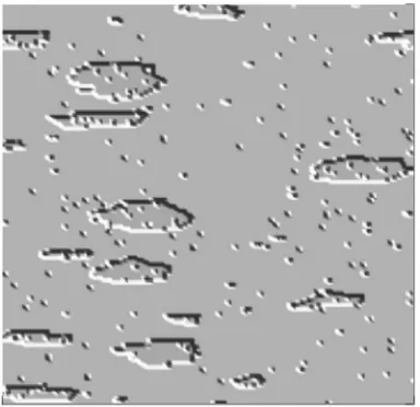
Next, we examine etching behavior again at 550 ° C but for higher oxygen pressurePO2= 8⫻10−7 Torr which serves
to enhance the formation of etch pits on terraces relative to step recession. Figure 7 shows a 100⫻100 nm2 region of a
vicinal Si共100兲surface revealing a mixed pit-nucleation and step-flow etching mode. This mode involves an alternation between nucleation of etch pits on TA terraces where the
dimer rows are parallel to the steps, and pure step recession on TB terraces where the dimer rows are orthogonal to the
steps. This behavior should be expected since the DV density will grow higher on the former terraces where DV’s cannot so easily reach and be incorporated at step edges, and thus nucleation of etch pits is enhanced. The etch pits tend to be aligned with the dimer rows, reflecting their preferred equi-librium elliptical structure.15 Note that the oxygen higher
pressure used in this simulation also produces a substantially higher density of oxide islands.
For completeness, in Fig. 8, we show simulation results for etching of a flat共singular兲Si共100兲 surface purely by pit nucleation and growth also at 550 ° C, but for lower PO2
= 2⫻10−8Torr to enhance pit size. In general, complete
shape equilibration is not expected on the time scale of etching,2,8,11 and shape fluctuations are significant.
Conse-quently, pits somewhat irregular although still reflecting their equilibrium elliptical structure elongated in the direction of the dimer rows.15Such irregular pits have been seen in STM
studies of etching on broad terraces.10 We have already
ob-served in Sec. IV that nucleation in this regime is intermedi-ate between far-from-equilibrium and near-equilibrium. In addition, we should also note that the details of the nucle-ation behavior should be impacted by the strong anisotropy in DV diffusion.42 Furthermore, growth behavior of
indi-vidual pits is expected to be determined by their associated “capture zones”2,11,43 from which they collect diffusing
DV’s. These capture zones will also reflect anisotropy in DV diffusion 关which is presumably much weaker in previous studies at very highT 共Refs. 2 and 11兲兴.
The various features predicted by our simulation model are in fact apparent in STM studies of the etching of vicinal Si共100兲.4,5 The initial preferential etching, i.e., faster
reces-sion, ofSB steps is clear, as is their pinning by some sort of
defect site to create fingers and the subsequent break off of fingers. See particularly Figs. 1 and 2 in Ref. 4, and Fig. 1 in Ref. 5. Clear evidence is provided that the defect pinning sites are directly related to oxygen, and are thus reasonably identified as oxide islands.4,5The behavior of the ratioRof
TA to TB terrace areas with exposure to oxygen at 600 ° C 共Ref. 5兲 is consistent with model predictions, as discussed above. An image of mixed-mode growth can be found in Ref. 12.
VI. DISCUSSION AND SUMMARY
Often etching or erosion processes are regarded as the inverse of growth. Thus, it is instructive to compare morpho-logical evolution described above for etching of vicinal Si共100兲 with growth modes and morphologies for MBE of atomic Si on vicinal Si共100兲. One finds various growth
[image:11.612.78.269.55.264.2]re-FIG. 7. Simulation image共100⫻100 nm2兲 showing alternating formation of etch pits共indicated by arrows兲onTAterraces and step flow acrossTB terraces at 550 ° C and PO2= 8⫻10−7Torr. Light colored regions are 共small兲 oxide islands, which occur at higher density than in Fig. 4.
FIG. 8. Simulation image共100⫻100 nm2兲showing etching of a flat Si共100兲surface at 550 ° C withPO2= 2⫻10−8Torr. The irregu-lar etch pits are elongated along the dimer row direction共which is horizontal in this image兲.
SIMULTANEOUS ETCHING AND OXIDATION OF… PHYSICAL REVIEW B72, 195420共2005兲
[image:11.612.341.533.57.243.2]gimes for Si MBE.14,29 共i兲 Island nucleation at low T of
300 ° C. 共ii兲 A mixed growth mode at 450 ° C initially in-volving step flow of adatoms across TB terraces to rapidly
advancingSBsteps, and island nucleation onTAterraces.共iii兲
Step flow at 500 ° C and high flux, where SB steps almost
catch up toSA steps creating near-double length TB terraces
separated by imperfect biatomic steps. Such steps areSA-like
in the sense that they cannot efficiently capture adatoms, so the adatom density builds up producing some island nucle-ation and a decrease in the relative populnucle-ation ofTBterraces. 共iv兲 Pure step flow at 500 ° C for low flux and at higherT, although perfect bistable steps do not form due to weak pin-ning effects 共or due to entropic step repulsion, which is dominant above 580 ° C兲.
Thus, the more rapid advance ofSBsteps in MBE, and the
corresponding enhancement of TB relative to TA terrace
population, is analogous to behavior seen in etching. Step flow growth would be observed in etching at 550 ° C or above共for lowerPO2兲if not for the strong pinning effects of oxide islands. The weak pinning effects in MBE produce rather different “fatter finger” morphologies than in etching. Entropic step repulsion will also be significant for etching at high enoughT. The mixed mode growth in MBE at 450 ° C mimics that in etching at 550 ° C for higherPO2. The shift of these growth modes to higher T for etching 共relative to MBE兲reflects the larger activation barrier for DV diffusion relative to Si adatom diffusion.
More recent studies of Si MBE on Si共100兲 argue that anisotropic diffusion produces an effective inverse ES barrier which induces a step bunching instability.44Such subtle
in-stabilities could in principle occur for etching, but in practice they do not have a chance to develop in our study as the surface morphology is dominated by strong pinning effects. An even closer analogy with etching of Si共100兲 is pro-vided by studies of step recession during ion sputtering of Si共100兲,45since sputtering produces surface vacancies which
can nucleate vacancy pits at lowerT, or diffuse to and erode steps at higherT.共Sputtering may produce other surface ad-species which play a role in surface evolution, although de-tailed characterization is not available.兲For sputtering, faster retraction of SB steps and dominance of TA terraces is
ob-served, just as in etching. It has been argued that anisotropic accommodation of vacancies beyond just anisotropy in dif-fusion is required for this behavior.46
In summary, our atomistic modeling of the etching and oxidation of vicinal Si共100兲, while still simplifying some as-pects of the process, has been quite successful in generating the main features of the evolving surface morphology as seen in STM studies. Anisotropic energetics guarantees distinct features of smoothSAand roughSBsteps. The kinetic model
recovers the fast retraction ofSB steps due to the anisotropic
accommodation of DV’s at step edges 共favoring SB steps兲.
Oxide islands pin the receding step edges. SB steps, which
are not very stiff, readily bend around these creating ex-tended fingers, one of the most dramatic features of the STM images. For higher etching rates共and also for lowerT兲, our modeling predicts a mixed mode of etching with island nucleation onTAterraces and step flow acrossTBterraces to SB steps. This feature was dependent on anisotropic DV
diffusion. In contrast, the existence of an island nucleation regime in the MBE modeling required formation of bi-atomic steps with low sticking coefficients for Si adatoms共as this simplified modeling did not incorporate anisotropic diffusion兲.29
ACKNOWLEDGMENTS
This work was supported by the SciDAC Computational Chemistry Program and the Division of Chemical Sciences of the U.S. Department of Energy 共USDOE兲. It was per-formed at Ames Laboratory operated by Iowa State Univer-sity under Contract No. W-7405-ENG-82.
APPENDIX A: KMC ALGORITHM
Our kinetic Monte Carlo共KMC兲simulation algorithm for the atomistic LG model of Sec. IV is primarily based on a Bortz-type rejection free approach,47where for each process
occurring with a specific rate, one maintains a corresponding list of eligible species. Then, at each KMC step, one chooses randomly from entries in these lists, weighted by the appro-priate rates. Thus, we maintain lists of isolated Si adatoms, divacancies, and O adatoms, and of O adatoms with one neighboring O 共each of which has a distinct diffusion rate兲. In addition, we maintain lists of isolated and step edge ad-dimers for each of the eight possible lateral coordinations
共since the hop rate depends on this coordination兲.
One complication is that the hop rates for Si ad-dimers also depend on the direction of the hop, and whether it is intralayer or interlayer. Rather than maintaining separate sublists for these different possibilities共which would require significantly more book keeping兲, we implement these pro-cesses with the correct physical rates by accepting some de-gree of rejection as follows. For each of the above eight classes of ad-dimers, a 共maximal兲 hop rate is initially as-signed given by exp关−共Edf+nw+ns兲兴. Then the actual
move will be executed with probability of 1, exp关−共Eds
−Edf兲兴, or exp关−1 / 2共Eds−Edf兲兴, when hops are 共i兲
intra-layer and along the direction of dimer row,共ii兲intralayer and orthogonal to the dimer row, and共iii兲interlayer, respectively. As described in Sec. III, we set Edf= 1.0 eV and Eds
= 1.3 eV. In a sense, the penalty for the initial choice diffu-sion barrier which may be too low is the possibility that the eventual move would be rejected.
Finally, we note that our simulations used periodic bound-ary conditions in the direction of the steps, and skewed pe-riodic boundary conditions in the direction orthogonal to the steps. For the latter, an adspecies exiting from the higher terrace on the right of the simulation images in Figs. 4 and 6, or 7, will reenter on the lower terrace on the left.
APPENDIX B: OTHER MODEL REFINEMENTS
detachment from step edges. Such an enhanced pathway in-troduces an additional parameter into the model. Thus, rather than perform a comprehensive analysis of this extended model, we just consider the case where the overall reaction rate for this pathway is comparable to that of the standard pathway. We also require that the total etch rate is compa-rable to that in the model of Sec. IV. We then ask if there is any discernable difference in the etch morphologies?
To select parameters in the extended model to achieve the desired behavior, we note that the density per site of diffusing Si ad-dimers has the form exp关−共w+s兲兴, so
the overall etch rate from reaction with these has the form exp关−共ESiO* +w+s兲兴, which should be compared with
exp关−ESiO兴 from the standard pathway. Thus, we choose
ESiO* =ESiO−w−s. Since we have two comparable
path-ways, we also increase barriers for both pathways by a small amount to reduce the rate for each by a factor of two. Then, simulation of the extended model reveals oxide cluster den-sity and oxygen uptake behavior essentially identical to the standard model of Sec. IV共as desired兲. Furthermore,
exami-nation of the etch morphologies reveals no significant differ-ence from those of the standard model.
Next, we comment on the treatment of nucleation of oxide islands, including possible enhanced nucleation at step edges. Our treatment of oxide nucleation is somewhat ad hoc, and certainly more input on atomistic energetics for this process would help to refine the modeling. Nonetheless, we can reasonably describe the observed oxide island density and oxygen uptake. However, the modeling presented here has not included a mild enhancement of nucleation of oxide islands at step edges, a feature quantified in one experimental study.37This feature has been implemented in our modeling,
but does not significantly change the behavior described in this study. Finally, we note that our modeling, similar to that of Ref. 6, does not produce the degree of saturation of the oxide island density observed in experiment. One possibility to closer match the latter would be to reduce the oxygen diffusion barrier so as to increaseLOto a value comparable
to the observed oxide island separation as this would inhibit oxide island nucleation.
1T. Engel, Surf. Sci. Rep. 18, 91共1993兲.
2J. B. Hannon, M. C. Bartelt, N. C. Bartelt, and G. L. Kellogg,
Phys. Rev. Lett. 81, 4676共1998兲.
3Fundamental Aspects of Silicon Oxidation, edited by Y. J. Chabal 共Springer, Berlin, 2001兲.
4J. V. Seiple and J. P. Pelz, Phys. Rev. Lett. 73, 999共1994兲. 5J. V. Seiple and J. P. Pelz, J. Vac. Sci. Technol. A 13, 772共1995兲. 6C. Ebner, J. V. Seiple, and J. P. Pelz, Phys. Rev. B 52, 16 651
共1995兲.
7J. V. Seiple, C. Ebner, and J. P. Pelz, Phys. Rev. B 53, 15 432 共1996兲.
8M. A. Albao, D.-J. Liu, C. H. Choi, M. S. Gordon, and J. W.
Evans, Surf. Sci. 555, 51共2004兲.
9M. Suemitsu, Y. Enta, Y. Miyanishi, and N. Miyamoto, Phys.
Rev. Lett. 82, 2334共1999兲.
10K. Wurm, R. Kliese, Y. Hong, B. Rottger, Y. Wei, H.
Nedderm-eyer, and I. S. T. Tsong, Phys. Rev. B 50, 1567共1994兲. 11M. C. Bartelt, J. B. Hannon, A. K. Schmid, C. R. Stoldt, and J. W.
Evans, Colloids Surf., A 165, 373共2000兲.
12J. L. Skrobiszewski, J. C. Moore, J. W. Dickinson, and A. A.
Baski, J. Vac. Sci. Technol. A 22共R兲1667共2004兲. 13H. Zandvliet, Rev. Mod. Phys. 72, 593共2000兲. 14B. Voigtlander, Surf. Sci. Rep. 43, 127共2001兲.
15N. C. Bartelt, R. M. Tromp, and E. D. Williams, Phys. Rev. Lett.
73, 1656共1994兲.
16D. J. Eaglesham, A. E. White, L. C. Feldman, N. Moriya, and D.
C. Jacobson, Phys. Rev. Lett. 70, 1643共1993兲.
17B. S. Swartzentruber, Y.-W. Mo, R. Kariotis, M. G. Lagally, and
M. B. Webb, Phys. Rev. Lett. 65, 1913共1990兲.
18A. Esteve, Y. J. Chabal, K. Raghavachari, M. K. Weldon, K. T.
Queeney, and M. Djafari Rouhani, J. Appl. Phys. 90, 6000 共2001兲.
19M. K. Weldon, B. B. Stefanov, K. Raghavachari, and Y. J.
Cha-bal, Phys. Rev. Lett. 79, 2851共1997兲.
20Y. J. Chabal, K. Raghavachari, X. Zhang, and E. Garfunkel, Phys.
Rev. B 66, 161315共R兲 共2002兲.
21C. H. Choi and M. S. Gordon, inComputational Materials
Chem-istry: Methods and Applications, edited by L. A. Curtiss and M. S. Gordon共Kluwer, Dordrecht, 2004兲, p. 125.
22C. H. Choi, D.-J. Liu, J. W. Evans, and M. S. Gordon, J. Am.
Chem. Soc. 124, 8730共2002兲.
23Y. Miyamoto and A. Oshiyama, Phys. Rev. B 41, 12 680共1990兲. 24Z. Zhang and H. Metiu, Phys. Rev. B 48, 8166共1993兲. 25Z. Zhang, F. Wu, H. J. W. Zandvliet, B. Poelsema, H. Metiu, and
M. G. Lagally, Phys. Rev. Lett. 74, 3644共1995兲.
26B. Borovsky, M. Krueger, and E. Ganz, Phys. Rev. Lett. 78, 4229 共1997兲.
27S. Clarke and D. D. Vvedensky, J. Appl. Phys. 63, 2272共1988兲. 28B. Voigtlander, T. Weber, P. Smilauer, and D. E. Wolf, Phys. Rev.
Lett. 78, 2164共1997兲.
29N. Kitamura, M. G. Lagally, and M. B. Webb, Phys. Rev. Lett.
71, 2082共1993兲.
30Y. W. Mo, J. Kleiner, M. B. Webb, and M. G. Lagally, Phys. Rev.
Lett. 66, 1998共1991兲.
31Q.-M. Zhang, C. Roland, P. Boguslawski, and J. Bernholc, Phys.
Rev. Lett. 75, 101共1995兲.
32C. Pearson, M. Krueger, and E. Ganz, Phys. Rev. Lett. 76, 2306 共1996兲.
33B. S. Swartzentruber, Phys. Rev. B 55, 1322共1997兲.
34D. G. Cahill and Ph. Avouris, Appl. Phys. Lett. 60, 326共1992兲. 35P. Jensen, H. Larralde, and A. Pimpinelli, Phys. Rev. B 55, 2556
共1997兲.
36J. A. Venables, Philos. Mag. 27, 693共1973兲.
37V. Brichzin and J. P. Pelz, Phys. Rev. B 59, 10 138共1999兲. 38H.-C. Jeong and E. D. Williams, Surf. Sci. Rep. 34, 171共1999兲. 39J. W. Evans and M. C. Bartelt, J. Vac. Sci. Technol. A 12, 1800
共1994兲.
40W. Theis and R. M. Tromp, Phys. Rev. Lett. 76, 2770共1996兲. 41The feature of our model that the direct DV diffusion pathway is
inoperative for the last hop producing aggregation of DV means
SIMULTANEOUS ETCHING AND OXIDATION OF… PHYSICAL REVIEW B72, 195420共2005兲
thenDVvalues are somewhat higher than if it was active. 42M. C. Bartelt and J. W. Evans, Europhys. Lett. 21, 99共1993兲. 43M. C. Bartelt, A. K. Schmid, J. W. Evans, and R. Q. Hwang,
Phys. Rev. Lett. 81, 1901共1998兲.
44J. Myslivecek, C. Shelling, F. Schaffler, G. Springholz, P.
Smi-lauer, J. Krug, and B. Voigtlander, Surf. Sci. 520, 193共2003兲. 45P. Bedrossian and T. Klitsner, Phys. Rev. Lett. 68, 646共1992兲.
46In our modeling, DV incorporation just at descending steps
effec-tively provides such an additional anisotropy. However, the claim in Ref. 45 that anisotropic diffusion of vacancies and iso-tropic incorporation at all steps would lead to depletedTA ter-races seems unfounded.
47A. B. Bortz, M. H. Kalos, and J. L. Lebowitz, J. Comput. Phys.