Development of Metal Oxide Solar Cells
through Numerical Modelling
Le Zhu
Doctor of Philosophy
awarded by
The University of Bolton
August, 2012
Acknowledgements
I would like to acknowledge Professor Jikui (Jack) Luo and Professor Guosheng Shao
for the professional and patient guidance during the whole research. I would also like
to thank the kind help by and the academic discussion with the members of solar cell
group and other colleagues in the department, Mr. Liu Lu, Dr. Xiaoping Han, Dr.
Xiaohong Xia, Mr. Yonglong Shen, Miss. Quanrong Deng and Mr. Muhammad Faruq.
I would also like to acknowledge the financial support from the Technology Strategy
Board under the grant number TP11/LCE/6/I/AE142J.
For my beloved parents
Abstract
Photovoltaic (PV) devices become increasingly important due to the foreseeable energy crisis, limitation in natural fossil fuel resources and associated green-house effect caused by carbon consumption. At present, silicon-based solar cells dominate the photovoltaic market owing to the well-established microelectronics industry which provides high quality Si-materials and reliable fabrication processes. However ever-increased demand for photovoltaic devices with better energy conversion efficiency at low cost drives researchers round the world to search for cheaper materials, low-cost processing, and thinner or more efficient device structures. Therefore, new materials and structures are desired to improve the performance/price ratio to make it more competitive to traditional energy.
Metal Oxide (MO) semiconductors are one group of the new low cost materials with great potential for PV application due to their abundance and wide selections of properties. However, the development of MO solar cells is very limited so far mostly due to the poor materials and poor understanding of the materials and devices. This research conducts a systematic numerical investigation on MO thin film solar cells. Various MO semiconductors are used to explore different structures and combinations for solar cells; and the effects of material properties and structures are optimised for the best performances.
For the ideal cases, it is found that a TiO2/CuO hetero-junction solar cell shows a
conversion efficiency of ~16% with the CuO film thickness only 1.5µm. When a back surface field layer, such as Cu2O, is added at the back of this device, the open circuit
voltage (VOC) can be improved by 70% without sacrificing short circuit current,
The effects of defects and interface states are then considered for more realistic cases as there exists vast amount of defects mostly due to oxygen/metal vacancies/interstitials in the films, and vast amount of interface states due to the large lattice mismatch of the two materials used. All defects and interface states in the solar cell layers, hetero-junction interfaces and metal/semiconductor contacts are found detrimental to the cells. For example, if the defect concentration in the CuO layer in TiO2/CuO structure is compatible to the acceptor concentration of 1x1016cm-3, the cell
efficiency would be reduced dramatically to 7%. With defect concentration even as low as 1x1013cm-3, the significant VOC improvements in the TiO2/CuO/Cu2O would be
reduced to an ignorable value. For interface states, they capture and recombine both electrons and hols passing through the hetero-junction interface, leading to deteriorated performance. The simulation shows that the interface states have a detrimental effect on the performance if its density is higher than 1012cm-2. However it was found that by increasing the difference of doping concentration in p-n junctions, the interface state effect minimized significantly.
Furthermore, it is found the optical reflection at hetero-junction interface may induce a serious conversion efficiency loss, if the n-type semiconductors and p-type semiconductors have very different refractive indices. For some MO devices such as TiO2/CuO and ZnO/Cu2O, the reflection rate is around 5%, while for other material
Table of Contents
Table of Contents ... IV
List of Tables and Figures ... VII
List of Abbreviations and Symbols ... XV
Chapter 1 Introduction ... 1
1.1 Background Information ... 2
1.2 Solar Cell Simulation Work, the Research Topic... 4
1.3 Thesis Structure ... 5
Chapter 2 Literature Review ... 8
2.1 History Background... 8
2.2 Modern PV Solar Cells ... 9
2.2.1 Sibased Solar Cells... 9
2.2.2 IIIV Compound Semiconductor Solar Cells ...14
2.2.3 Chalcogenide Semiconductor Solar Cells ...15
2.2.4 Metal Oxide Semiconductor Solar Cells ...18
2.3 Device Simulation ... 22
2.3.1 Key Fundamental Equations and Simulation Tools ...22
2.3.2 OneDimensional Device Simulation ...26
2.4 Summary ... 34
Chapter 3 The Semiconductor Theory Contained in the Simulation Approach ...50
3.1 Materials ... 50
3.1.1 Energy bands and material classification ...50
3.1.2 Intrinsic semiconductors ...52
3.1.3 Extrinsic semiconductors ...53
3.2 Joining Materials Together ... 54
3.2.1 Pn junction formation ...55
3.2.2 Band offsets at interfaces ...57
3.2.3 Interfacestates (ISt) density...60
3.3 Carrier Generation, Transportation and Recombination ... 60
3.3.2 Generation and recombination ...62
3.3.3 Continuity equations ...64
3.3.4 Optical modelling ...66
3.4 Solar cell efficiency ... 67
3.5 Summary ... 68
Chapter 4 Silicon Solar Cell Simulation ...70
4.1 Simulation Settings ... 70
4.2 Results and Discussion ... 72
4.2.1 Validation of simulation packages ...72
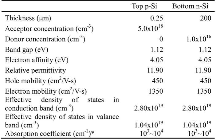
For the purpose of validation of simulation packages, a simple solar cell geometry is used as the testing structure. Comparison between simulation results and analytical results produced by theories and equations in Chapter 3 is made in this section. For a simple double layered solar cell geometry shown in Fig.4.1, the simulation settings for both of the layer can are list in Table 4.2. ...72
4.2.2 Ideal situation ...75
4.2.3 Nonideal situation ...80
4.3 Summary ... 80
Chapter 5 Ideal Metal Oxide Hetero-junction Solar Cells ...83
5.1 Simulation Settings ... 84
5.1.1 Simulation settings for bandgap engineering...85
5.1.2 Simulation settings for WA and WAV structures ...86
5.2 Results and Discussion ... 87
5.2.1 TiO2 bandgap engineering ...87
5.2.2 WA solar cell with various metal oxide semiconductors...93
5.2.3 WAV solar cell and Vlayer BSF effects...105
5.3 Summary ... 114
Chapter 6 Metal Oxide Hetero-junction Solar Cell with Defects and Interface States ... 118
6.1 Simulation Settings ... 119
6.2 Results and Discussions... 121
6.2.1 TiO2/CuO structure defect problems ...122
6.2.2 TiO2/CuO/Cu2O structure defect problems ...129
6.2.3 Interface states problems ...132
Chapter 7 Metal Oxide Schottky Barrier Solar Cells ... 143
7.1 Simulation Settings ... 144
7.2 Results and Discussion ... 145
7.2.1 Schottky barrier solar cell thickness ...146
7.2.2 Barrier height for both of the contacts ...148
7.2.3 Back surface field effect for MSV structure ...151
7.2.4 Comparison of CuO and Cu2O Schottky barrier solar cells ...153
7.3 Summary ... 155
Chapter 8 Hetero-junction Solar Cell Interfacial Optical Reflection ... 158
8.1 Reflection at the Internal Interfaces ... 159
8.2 Error Source of the Reflectance in Simulation ... 163
8.3 Summary ... 165
Chapter 9 Conclusions and Future Work ... 168
9.1 Conclusions ... 168
9.2 Future work ... 171
APPENDIX A ... 175
List of Tables and Figures
Tables
Table 2.1 Energy bandgaps of crystalline silicon and amorphous silicon alloys.
Table 2.2 Properties of some selected metal oxide semiconductors. (*Note: EG for
energy bandgap, Xe for electron affinity).
Table 4.1 Parameter setting ranges for Si-cells. The data in the brackets are constant
settings for the model when varying that parameter. The sequence is (p-layer
thickness, n-layer thickness, p-layer doping concentration, n-layer doping
concentration).
Table 4.2 Device modelling parameter settings for each layer in p/n Si solar cell in
Fig.4.1.
Table 5.1 TiO2 bandgap engineered solar cell variable settings. The values in three
brackets in each table cell represent: (top-layer thickness, bottom-layer
thickness) (top-layer doping concentration, bottom-layer doping concentration)
and (top-layer EG, bottom layer EG). Parameters with ‘~’ are the variables
while all other parameters are set constant.
Table 5.2 Device modelling parameter settings for each layer in WA and WAV
structures.
Table 5.3 Variable setting ranges and the corresponding constant settings. (Parameters in
the brackets are in the sequence of layer thickness, A-layer thickness,
W-layer doping concentration and A-W-layer doping concentration).
Table 6.1 Simulation settings for each material (ideal starting model).
Table 6.2 Simulation settings for defects.
Table 6.3 Simulation settings for interface states.
Table 8.1 Relative permittivity and refractive index (at 550nm wavelength) of some
Figures
Figure 1.1 Global energy transition predicted by German Advisory Council on Global
Change, 2003.
Figure 1.2 Typical solar cell structure, on N-Type Silicon substrates.
Figure 1.3 Mechanism of band gap engineering (EC).
Figure 2.1 Typical screen-printed first-generation solar cell.
Figure 2.2 The OECO-MIS-IL Schottky barrier Si solar cell. (the inversion layer is the
metal layer).
Figure 2.3 The typical structure of thin-film polycrystalline silicon solar cell fabricated by
Yamamoto et al and Gall et al.
Figure 2.4 The structure of HIT solar cell developed by Sanyo Ltd.
Figure 2.5 Typical configuration of CdS/CdTe hetero-junction solar cell.
Figure 2.6 Typical CIGS solar cell configuration and band diagram.
Figure 2.7 The TCO/CuO/C60/Al solar cell configuration.
Figure 2.8 Two cell configurations and the corresponding band diagrams.
Figure 2.9 Graded CIGS band-gap profiles Song et al. proposed.
Figure 2.10 Simulated outputs of tandem cells consist of various numbers of sub-cells.
Figure 3.1 Band diagram for (a) insulator, (b) semiconductor and (c) conductor.
Figure 3.2 P-n junction formation, and the diffusion & drift phenomena.
Figure 3.3 Charge and electric field distribution of (a) abrupt junction and (b) linearly
graded junction.
Figure 3.4 Band diagrams of two semiconductors when they: (a) are isolated, and (b)
form a hetero-junction.
Figure 3.5 Band diagram of isolated (a) and junction (b) of metal and semiconductor;
charge (c) and electric-filed (d) distribution in the junction.
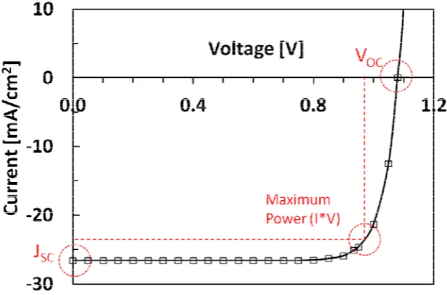
Figure 3.6 I-V curve of a TiO2/CuO/Cu2O solar cell generated by AFORS-HET software
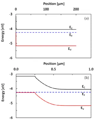
Figure 4.2 Band diagram of validation Si solar cell geometry produced by AMPS-1D. (a)
the overall band diagram, and (b) the detailed diagram at the p/n junction area.
Figure 4.3 I-V curve of the validation Si solar cell produced by AMPS-1D.
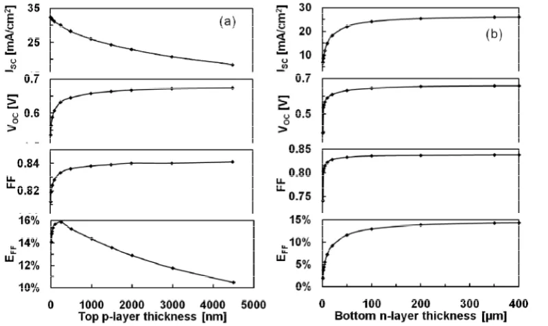
Figure 4.4 Performances vs. layer thickness of (a) p-type top layer and (b) n-type bottom
layer.
Figure 4.5 Performances vs. doping concentration of (a) p-type top layer and (b) n-type
bottom layer.
Figure 4.6 Solar cell performances v.s. BSF barrier height.
Figure 4.7 Performance affected by the concentration of (a) donor-like defects and (b)
acceptor-like defects in top p-type layer.
Figure 4.8 Performance affected by the concentration of (a) donor-like defects and (b)
acceptor-like defects in bottom n-type layer.
Figure 4.9 Current density components in ideal device.
Figure 5.1 Starting structures for the simulation study in this chapter: a) bandgap
engineering –based on TiO2 alloying; b) Window/Absorber (WA) structure
with emphasis on TiO2/CuO system; and c)
Window/Absorber/Voltage-Enhancer (WAV) structure with emphasis on TiO2/CuO/Cu2O.
Figure 5.2 TiO2 two-layered structure, layer thickness effects: (a) top n-type layer and (b)
bottom p-type layer.
Figure 5.3 TiO2 cell performances vs. (a) top layer doping concentration and (b) bottom
layer doping concentration.
Figure 5.4 TiO2 cell performances vs. (a) top layer bandgap, and (b) bottom layer
bandgap.
Figure 5.5 Performances vs. top layer thickness (100nm~500nm) when the
top-layer/bottom-layer EG are set 1.6eV/1.55eV.
Figure 5.6 Band diagrams of solar cells in Fig.5.5 when top layers are set 100nm (a) and
500nm (b).
Figure 5.8 The effects of the W-layer (a) and A-layer (b) thickness on the performances
of the WA cell.
Figure 5.9 The effects of W-layer (a) and A-layer (b) concentration on the cell
performances of WA cell.
Figure 5.10 Band diagram for different A-layer doping levels: curves (a) 1x1018 cm-3; (b)
5x1016 cm-3; (c) 5x1014 cm-3with a constant W-layer doping concentration at
1x1019 cm-3.
Figure 5.11 Band diagram of ZnO/Cu2O solar cell.
Figure 5.12 Thickness effects of (a) ZnO W-layer and (b) Cu2O A-layer.
Figure 5.13 Doping concentration effects of (a) ZnO W-layer and (b) Cu2O A-layer.
Figure 5.14 Cu2O A-layer doping concentration effect when conduction band offset
ΔEC=0eV.
Figure 5.15 Results of band offset (qχCuO – qχTiO2=-0.9eV~+0.7eV) simulation.
Figure 5.16 Band structures for various conduction band offset, ΔEC, within WA structure.
Figure 5.17 Performances vs. absorber A-layer band-gap in WA structure.
Figure 5.18 Band diagram of WAV solar cell (TiO2/CuO/Cu2O).
Figure 5.19 Performances vs. V-layer thickness for different A-layer thickness: (a) 800nm,
(b) 100nm.
Figure 5.20 The CuO (A-layer) thickness effects in TiO2/CuO/Cu2O WAV structure.
Figure 5.21 Effects of V-layer bandgap and hence, ΔEC on WAV cell performances.
Figure 5.22 VOC v.s. V-layer bandgap for various V-layer doping concentration.
Figure 5.23 Band diagram (a) and electric field (b) near A/V interface when V-layer
EG=1.4V (<EGC).
Figure 5.24 VOC v.s. V-layer bandgap for various A-layer thicknesses (same settings as in
Fig. 5.23).
Figure 5.25 Current components of WA and WAV structures under short circuit condition.
Figure 6.2 Band diagrams of WA cell with (a) 1x1018cm-3 acceptor-like defects and (b)
1.1x1019cm-3 acceptor-like defects in the n-type W-layer (doping concentration
=1x1019cm-3).
Figure 6.3 Performances vs. acceptor-like defects (a) and donor-like defects (b) in CuO
A-layer concentration.
Figure 6.4 Band diagram of WA solar cell with donor-like defect concentration of
(a)1x1014cm-3 and (b)1x1017cm-3 in the p-type A-layer(acceptor doping concentration is 1x1016cm-3).
Figure 6.5 Solar cell performances vs. CuO A-layer doping concentration, when A-layer
is set constant acceptor-like defect at 5x1015cm-3 (black squares) and when
A-layer is set free of defects (red triangles).
Figure 6.6 Solar cell performances vs. the energy level (above EV) of defects in p-type
A-layer with 1x1016cm-3 acceptor concentration. (Defects are set acceptor-like,
Gaussian distribution and 5x1015cm-3 concentration).
Figure 6.7 Performances vs. acceptor-like defects-induced p-type A-layer doping
concentration.
Figure 6.8 Effects of acceptor-like defect concentration in the V-layer.
Figure 6.9 Solar cell performances vs. A-layer acceptor-like defect density for WA and
WAV structure.
Fig.6.10 JSC, VOC, FF and EFF vs. density of acceptor-like ISt at W/A interface on WA
solar cell performances. (The energy level of ISt are written as EIST above EV
of TiO2 W-layer, equivalent to EIST-1.58eV above EV of CuO A-layer).
Figure 6.11 Performances of solar cells with different W-layer doping concentration, vs.
interface states density.
Figure 6.12 A/V interface ISt density effects at different V-layer doping concentration:
1x1016cm-3 (black hollow square) and 1x1019cm-3 (red cross).
Figure 6.13 I-V curves of ideal WAV cells when V-layer is doped at 1x1016cm-3 (black
Figure 6.14 I-V curves of solar cells with different V-layer doping concentration: (a)
1x1016cm-3 and (b) 1x1019cm-3 when the ISt are able to effectively capture
‘both electrons and holes’ (black hollow squares), ‘electrons-only’ (red cross)
and ‘holes-only’ (blue hollow triangles).
Figure 7.1 Schematic diagrams of MS (a) and MSV (b) Schottky barrier solar cell
structures.
Figure 7.2 Band diagrams of MS (a) and MSV (b) structure solar cells.
Figure 7.3 Cell performances vs. CuO layer thickness (front illumination and back
illumination).
Figure 7.4 Cell performances vs. Schottky barrier height. All the parameters increase with
the barrier height.
Figure 7.5 Cell performances vs. back contact barrier height (negative BH value
represents an Ohmic contact with heavily-doped layer).
Figure 7.6 Band diagrams for various situations of the back contact: (a) -0.3eV; (b)
0.1eV.
Figure 7.7 Comparison of MS (dots), MSV (square) and WAV (triangle) cell
performances as a function of CuO thickness. Cu2O is assumed to have
EG=2.1eV and 100nm thickness.
Figure 7.8 Carrier generation rate in illuminated MSV solar cell. The generation rate in
V-layer is about six orders of magnitude smaller than that in CuO layer.
Figure 7.9 Comparison of ideal CuO and Cu2O Schottky barrier solar cells. (The data for
CuO MS cell is the same as MS plot in Fig.7.7, and doping concentration is
1016/cm3 for both the materials).
Figure 7.10 Results for CuO MS solar cell with an additional 5nm Cu2O layer at the front,
and the settings are the same as in Fig.9: (a) band diagram (only up to 500nm
is shown for easy view) and (b) I-V characteristic which has a strange
Figure 8.1 Schematic drawing for reflection and refraction at the interface of a
hetero-structure.
Figure 8.2 Reflectance as a function of the window layer refractive index for
hetero-junction solar cells with various A-layer refractive index.
Figure 8.3 Reflectance vs. wavelength for some hetero-junction systems.
Figure 8.4 Comparison of I-V curves of TiO2/CuO cells using different refractive indices
measured and calculated from the permittivity.
Figure AA1 AMPS-1D main user interface.
Figure AA2 Voltage biasing input: -1.50V~1.50V, which is the I-V measurement range.
Figure AA3 Illumination intensity defined by ‘LAMBDA’ and ‘FLUX’, material optical
absorption coefficient defined by ‘ALPHA’, and optical absorption edge
defined by ‘Eopt’
Figure AA4 Simulation temperature settings
Figure AA5 Front and back contact settings.
Figure AA6 Layer information settings.
Figure AB1 AFORS-HET main user interface.
Figure AB2 Structure define.
Figure AB3 Front Contact settings.
Figure AB4 Layer property definition.
Figure AB5 Define the defects.
Figure AB6 Define of interface states.
List of Abbreviations and Symbols
Abbreviations
A-layer Absorption layer
BH Barrier height
BSF Back surface effect
ISt Interface states
M/S Metal/Semiconductor
MSV Metal/Semiconductor/Voltage-enhancement
MO Metal oxide
S/S Semiconductor/Semiconductor
SBH Schottky barrier height
SRH Shockley-Read-Hall recombination process
V-layer Voltage-enhancement layer
WA Window-Absorber double-layer single hetero-junction structure
WAV Window-Absorber-Voltage-enhancement triple layer, double hetero-junction
structure
W-layer Window layer
Symbols (English letters)
cn Electron capture cross-section for a recombination centre
cp Hole capture cross-section for a recombination centre
Dn Electron diffusivity
Dp Hole diffusivity
EC Bottom of conduction band
EF Fermi energy level
EG Energy bandgap of semiconductors
EGC Critical energy bandgap value for Voltage-enhancement-layer in WAV
structure
EV Top of valence band
F(E) Fermi-Dirac distribution
FF Fill factor (solar cell)
G Carrier generation rate
h Planck constant
JSC Short circuit current (solar cell)
Jn Electron current
Jp Hole current
k Boltzmann constant
l Mean free path
Ln Electron diffusion length in p-type semiconductor
Lp Hole diffusion length in n-type semiconductor
m0 Electron rest mass
mn Effective mass of electrons
mp Effective mass of holes
n Electron concentration
ni Intrinsic carrier concentration
NA Acceptor doping concentration
NC Effective density of states in conduction band
ND Donor doping concentration
NV Effective density of states in valence band
p Hole concentration
q Elementary charge
RE Reflection coefficient of light at an interface Sr Surface recombination speed
T Temperature (in Kelvin) vth Average thermal velocity
Vbi Build-in electric field
VOC Open circuit voltage (solar cell)
W Depletion region width
Symbols (Greek letters)
α Absorption coefficient ε Relative permittivity ξ Electric field
κ Attenuation coefficient of light, related to absorption coefficient α μn Electron mobility
μp Hole mobility
σ Capture cross section (recombination centres to carriers) τc Mean free time
Ψ Electrostatic potential
qΧe Electron affinity of semiconductors
qΦM Work function of metal
qΦS Work function of semiconductor
Chapter 1 Introduction
In the progress of human society, each level of civilization could be indicated by the
resources of energy and format of power. The main energy resource in Ancient Age is
human physical power, such as hunting, gathering and human-powered agriculture,
etc. During both feudal and enlightenment ages, human power and animal power are
the main power format, with some simple use of fossil and renewable energies, such as
wood, coal, wind mills and water mills. With the uplift into industrial age, fossil
energy, for example; coal, natural gas and oil began to take the lead in global energy
consumption, in the format of heat in steam engine and modern engines. From
Twentieth century to the present, electricity becomes a main energy format in the
modern electrical age, converted from various energy resources which include fossil
energy and some renewable energy.
However, due to the foreseeable running out of fossil fuels and related environmental
problems, including air pollution and global warming, man-kind has started to develop
clean renewable energy resources. Hydropower, nuclear power, wind power,
geothermal power, tidal power, solar power and biomass, etc. were introduced and are
still being developed as future energy options to replace fossil fuels. Of these
renewable energy formats, solar power is widely considered as one of the key ones for
the 21st century, due to its abundant and wide-accessible characteristics. Fig.1.1 shows
a prediction of the global energy consumption and composition for 21st century by the
German Advisory Council on Global Change in 2003 [1]. The Council indicates that 25% of global energy consumption in 2050 and even up to 65% by the end of 21st
century will be provided by the renewable energy, especially solar photovoltaic
energy. This survey gives the general idea of solar photovoltaic energy being vitally
Nowadays, photovoltaic (PV) solar cells are widely available for practical applications.
Solar power plants and domestic roof top solar panels can be found in many places
around the world. Solarbuzz, a solar market research and analysis group, has
demonstrated that the global PV market size increased by 139% pa, to 18.23GW in
2010, Worthing £82 billion [2]. The energy transition evolution as predicted seems to be moving faster and faster and will gradually lead the world into the
renewable-low-carbon energy era.
Figure 1.1 Global energy transition predicted by German Advisory Council on Global Change, 2003 [1].
1.1 Background Information
Photovoltaic (PV) solar cells are the kind of devices which transform the energy of
photons from solar spectrum directly into electricity. The core of PV solar cells is a p-n
junction, a metallurgical connection between a p-type semiconductor and n-type
semiconductor. This junction provides a built-in electrical field, which separates
electrical carriers activated by photons and transports them to the two cell terminals
coloured n-type silicon and yellow coloured p-type silicon is the p-n junction in this
structure. Other parts, such as the blue oxide anti-reflection layer and P+ back surface
field layer can enhance the performance of the cells or solve various technical
problems.
Figure 1.2 Typical solar cell structure, on N-Type Silicon substrates [3].
Currently, the majority of the solar cells are manufactured using silicon: single
crystalline, polycrystalline and amorphous. They are different in manufacturing cost
and performance due to the perfection levels of the materials. As a result of silicon, a
low optical absorption rate is shown, it is always necessary to manufacture solar cells
at a thickness of several hundred micrometers and hence lots of materials are
consumed. Apart from silicon solar cells, III-V semiconductors, II-VI compounds and
metal oxide semiconductors in thin film structured solar cells have either been
commercialized or are being developed. However, all of the solar panels now available
are either still too expensive, low in material storage or toxic to replace traditional
fossil energy. Therefore the search for low-cost materials, material-saving structures
and low-cost-easy processes is always ongoing.
Metal oxide semiconductors, both abundant and cheap, are considered to be a
sustainable group of the future PV materials. They have a wide spread of energy
bandgap to allow flexible combinations for various structures. For example, ZnO, a
natural n-type semiconductor with a wide energy bandgap over 3.0eV is suitable for
the fabrication of solar cell window layers as it is transparent to most of solar
electrode due to its perfect conductivity and transparency characteristics. Furthermore,
Cu2O and CuO, natural p-type semiconductors with an energy bandgap about 2.1eV
and 1.2~1.8eV, can absorb a considerable proportion of the solar spectrum effectively
within only several micrometers thickness. Therefore, they are candidate materials for
the absorption layer of thin film solar cells.
Apart from the natural properties, the bandgap value of some metal oxides could be
engineered manually by introducing some foreign elements. TiO2, for example, has a
natural bandgap of 3.0~3.2eV and can absorb only the ultraviolet part, about 5%, of
the solar spectrum. It could be doped or alloyed, most currently, with other elements to
reduce the bandgap to 2.9eV, 2.6eV, 2.2eV and 1.5eV to allow much more solar
absorption [4-10]. As shown in Fig.1.3, this bandgap engineering is mostly realised by the widening of mini-energy bands to merge with either conduction band or valence
band so hence the miniband edge becomes the new band edge. The bandgap, therefore,
is engineered as desired.
Figure 1.3 Mechanism of band gap engineering (EC).
1.2 Solar Cell Simulation Work, the Research Topic
By using various candidate semiconductors, researchers can develop various solar cells
in a wide range of structures. However, to save development costs, before the practical
work commences a simulation study is always needed for the materials selection and
For this reason, various solar cell simulation software have been developed around the world, and many others are in development. There are generally two kinds of models, first-principal simulation and neural-network simulation. The former one is usually used in simple solar cell simulation, the mechanisms of which are understood well in the early stage of device development. The latter one is always used for the performance predictions of complex structures such as multi-junction cells and solar arrays; the interference factors of which are massive and are thus, difficult to be considered comprehensively. These simulation tools make huge contributions during the development of solar cells with new materials and new structures.
This thesis records a systematic, first-principal simulation study of solar cell devices by using various candidate semiconductors, mainly consisting of natural or bandgap engineered metal oxides in various structures. The solar cell performances of these materials and structures are predicted and optimised for fabrication work. Nevertheless, at the same time, the understanding of functions of layers in solar cells is deepened. Therefore, guidance is drawn for cell fabrications and future solar cell designs.
1.3 Thesis Structure
This thesis presents the whole PhD study in the following parts: Introduction; Literature Review; The Semiconductor Theory Contained in the Simulation Approach; Silicon Solar Cell Simulation; Ideal Metal Oxide Hetero-junction Solar Cell; Metal Oxide Hetero-junction Solar Cell with Defects and Interface States; Metal Oxide Schottky-barrier Solar Cells; Hetero-junction Solar Cell Interfacial Optical Reflection and Conclusions and Future Work.
Chapter 3 The Semiconductor Theory Contained in the Simulation Approach: The simulation tools, AMPS-1D and AFORS-HET will be introduced. In addition, some basic theory and equations for semiconductor physics and solar cell physics, used in the simulation, will be presented.
Chapter 4 Silicon Solar Cell Simulation: This chapter is about a brief simulation study of well understood Si-solar cells. By the comparisons to existing Si-cells and theory, the understanding to solar cell principles can be deepened and the simulation tools could be calibrated.
Chapter 5 Metal Oxide Hetero-junction Solar Cell Simulation (Ideal): This is one of the main parts of this study, concentrating on the study of solar cell structures. In this Chapter, various MO solar cells will be simulated, including TiO2 bandgap-engineered
solar cells, TiO2/CuO solar cell, ZnO/Cu2O solar cell and TiO2/CuO/Cu2O solar cell.
All of these solar cells are in Window/Absorber (WA) or
Window/Absorber/Voltage-enhancer (WAV) structures. The functions and mechanisms of each layer will be
studied and understood. The feasibility of MO solar cell will be discussed.
Chapter 6 Metal Oxide Hetero-junction Solar Cell with Defects and Interface States: Chapter 5 discussed the ideal metal oxide (MO) solar cell performances and
application. This chapter will present a simulation study on MO solar cell considering defects and interface states which are serious practical problems for hetero-junction solar cells under development. Based on the study, the functions of defects and interface states will be understood, and relevant principals will be summarized for design and fabrication in the future.
Chapter 7 Metal Oxide Schottky Barrier Solar Cell Simulation: As another important part of the study, this Chapter is a full record of systematic simulation study on Schottky barrier solar cells, similar to Chapter 5, and still based mainly on metal oxide semiconductors.
considerable error to the output. Comparison of practical and simulation results of various solar cells will be discussed, in detail, within this Chapter.
Chapter 9 Conclusions and Future Work: The whole research and the important understandings of solar cells, conducted from the research, are summarized. Therefore guidance for solar cell fabrication and future invention and design will be concluded. Future work based on this research is proposed.
References
1 WBGU, German Advisory Council on Global Change, 2003
2 Solarbuzz, Global PV Market,
http://solarbuzz.com/facts-and-figures/market-facts/global-pv-market, 2010
3 High-Efficiency Solar Cell on N-Type Silicon Substrates, University of New South Wales,
Sydney, Australia, http://www.pv.unsw.edu.au/Research/heeg_High_Eff_N.asp, 2012
4 Y. Nakano, T. Morikawa, T. Whwaki and Y. Taga, Band-gap Narrowing of TiO
2 Films
induced by N-doping, Physica B: Condensed Matter,376-377 (2006), pp. 823-826 5 Y.C. Hong, C.U. Bang, D.H. Shin, H.S and Uhm, Band gap Narrowing of TiO
2 by Nitrogen
doping in Atmospheric Microwave Plasma, Chemical Physics Letters, 413 (2005), pp.
454-457
6 L. Wan, J.F. Li, J.Y. Feng, W. Sun and Z.Q. Mao, Anatase TiO
2 Films with 2.2 eV Band gap
Prepared by Micro-arc Oxidation, Materials Science and Engineering: B, 139 (2005),
pp.216-220
7 Y. Nakano, T. Morikawa, T. Ohwaki and Y. Taga, Origin of Visible-light Sensitivity in
N-doped TiO2 Films, Chemical Physics, 339 (2007), pp. 20-26
8 V. Nadtochenko, N. Denisov, A. Gorenberg, Y. Kozlov, P. Chubukoy, J.A. Rengifo, C.
Pulgarin and J. Kiwi, Correlations for Photocatalytic Activity and Spectral Features of the Absorption Band Edge of TiO2 modified by Thiourea, Applied Catalysis B: Environmental, 91 (2009), pp. 460-469
9 F. Dong, W. Zhao, Z. Wu and S. Guo, Band Structure and Visible LIght Photocatalytic
Activity of Multi-type Nitrogen doped TiO2 Nanoparticles Prepared by Thermal
Decomposition, Journal of Hazardous Materials162 (2009), pp. 763-770
10 I. Takahashi, D.J. Payne, R.G. Palgrave and R.G. Egdell, High Resolution X-ray
Photoemission Study of Nitrogen doped TiO2 Rutile Single Crystals, Chemical Physics
Chapter 2 Literature Review
2.1 History Background
Invented in the 19th century, photovoltaic solar cells didn’t become practical until 1954, producing a conversion efficiency of approximately 6% [1]. It was made of a thin layer of p-type silicon (<0.0001 inch) on an n-type silicon substrate. Almost at the same time, the early development in thin film solar cell was conducted by Reynolds et al [2] on cross-section illumination of a 3mm thick CdS sample, producing an open-circuit voltage of 0.4V and a short-open-circuit current of 15mA/cm2 in 1954. Silicon solar cell was then first applied on satellite Vanguard 1 in 1958 [3]. Due to the great success achieved by using solar cells, many other satellites were also designed to be powered by solar PV energy.
The intensive effort for wide-spread terrestrial application of solar cells, due to the fossil energy crisis, was started to be made from the 1970s [4]. The research at the time was not only on improving performance/cost ratio of silicon solar cells, but also on developing new material systems and structures, such as GaAs, AlGaAs, CdS, CdTe, indium tin oxide (ITO) , Cu2O, InP, polymers etc. in tandem,
Metal/Insulator/Semiconductor (MIS), etc structures [5-20]. In the 1980s and 1990s
2.2 Modern PV Solar Cells
In the past 20 years, the technologies have been developed and the fabrication cost has been reduced significantly for many solar cells. Silicon, III-V semiconductors and chalcogenide compounds solar cells are widely available. Due to the still high energy-production costs compared to fossil fuels and un-sustainable resources of some semiconductors, some other substitute semiconductors such as metal oxides and polymers are being developed.
2.2.1 Si-based Solar Cells
Silicon is an indirect bandgap semiconductor with an energy bandgap of 1.12eV [21]. The materials used in PV application can generally be classified into single-crystalline, poly-crystalline and amorphous silicon.
2.2.1.1 Single-crystalline silicon solar cells
Generally single-crystalline silicon solar cells were fabricated on single-crystalline silicon wafers, and the electrodes were deposited by using screen printing technology, as shown in Fig.2.1
Figure 2.1 Typical screen-printed first-generation solar cell [22].
achieve high conversion efficiency >18% [22-25]. Zhao et al. [26] also reported recently an efficiency of 24.5% achieved on the so-called ‘passivated-emitter, rear locally/totally (singly)/totally (doubly) diffused’ cell structures using various silicon substrates with thickness of 250~400μm. The best performance was achieved from the cells of 400μm Si-substrate with an open circuit voltage, VOC, of ~704mV, short circuit
current density, JSC, of ~41.6mA/cm2, fill factor, FF, of ~0.835, and conversion
efficiency, EFF,of ~24.5%. These advanced contact structures and surface passivation
techniques have made the cell performance close to the theoretical limit of 29~31% [27-29] for the conventional single junction silicon solar cell.
Many single junction silicon solar cells have a heavily doped back surface field (BSF)
layer [22-26,30,31], similar to the bottom p+ layer shown in Fig.2.1. It is found the
VOC, JSC, FF and hence, EFF can be improved by introducing this BSF effect layer. A
large amount of work has been done to understand the mechanism of this BSF effect. Experimentally, Godlewski et al. [32] reported the BSF effect can only be significant if the distance between the p/n junction and the BSF layer is smaller than approximately 3 times of minority carrier diffusion length in the absorption layer. Theoretically, Singh and Jain [33] explained the BSF effect most successfully as followed: the BSF layer can block and reflect minority carriers to contribute to VOC. The effectiveness of
the blocking and reflection effects may vary depending on the comparison between minority carrier concentration and doping concentration, or the distance between BSF layer and p/n junction.
Apart from the main body of the cell, some additional structures such as the pyramid-shaped anti-reflection coating and optical reflective rear metal contacts are also used to improve the performance to the theoretical limit. With these structures, the light can be trapped effectively within the cell maximum 40 times compared to those without the structures [34,35].
Apart from p-n junction type solar cells, metal/semiconductor (MS) Schottky type and
metal/insulator/semiconductor (MIS) type structured solar cells have been developed
solar cells, such as simple structure, simple fabrication process, low temperature processing, reasonably good efficiencies, limited problems from the interface states introduced by semiconductor lattice mismatch etc [41-48], but these have lower efficiencies.
Figure 2.2 The OECO-MIS-IL Schottky barrier Si solar cell. (the inversion layer is the metal layer) [40].
2.2.1.2 Poly-crystalline and amorphous silicon solar cells
In order to reduce the cost of PV solar cells, polycrystalline and amorphous silicon materials have been developed to be applied in various techniques. For solar cells it is always necessary to texture the surface to achieve good performances and it is the same for solar cells on polycrystalline silicon wafers [49]. Efficiency was achieved of 19.8% (VOC~654mV, JSC~38.1mA/cm2, FF~0.795) on a 260μm thick wafer with a
honeycomb surface texture by Zhao et al. [50] in 1998. The conversion efficiency of mass produced poly-crystalline solar cells varies from 12% to 15% [27].
Poly-crystalline silicon is also used for thin-film structured cells, the thickness of which can be reduced to several micrometers on low-cost substrates, hence reducing the fabrication cost significantly. Yamamoto et al. reported that a stabilized efficiency of 12% is achieved on a-Si:H/poly-Si/poly-Si structured cells with a thickness of approximately 1.5μm, which is fabricated by using plasma chemical vapour deposition (CVD) on a glass substrate, as shown in Fig.2.3 [51]. Recently, CSG Solar Company
has demonstrated a PV solar cell module made of poly-crystalline silicon on glass with an efficiency of 10.4% using solid-phase crystallization (SPC) technique [52].
1-2μm, close to the cell thickness. This means although the solar cells are poly-crystalline, the carriers would travel in single crystals in the vertical direction, facing limited interface barriers caused by grain boundaries. In order to improve poly-crystalline silicon grain quality and hence thin film solar cell performance, seed layers were introduced by Gall et al. [53] The cell was fabricated with the structure shown in Fig.2.3 showing an efficiency of 5.8% (VOC~570mV, JSC~13.3mA/cm2 and FF~0.76).
The cell has an absorber thickness of about 1800nm, a p+ back surface field seed layer
thickness of 375nm.
Figure 2.3 The typical structure of thin-film polycrystalline silicon solar cell fabricated by Yamamoto et al (left) [51] and Gall et al (right) [53].
Due to its very low carrier mobility (<1cm2/V-s) [54] and high absorption coefficient (about hundreds of times higher than that of crystalline silicon), amorphous silicon is usually used to fabricate solar cells in p-i-n or n-i-p thin film structure. Due to the amorphous nature, the material always shows a very high density (up to 1019/cm3) of defects, which reduces solar cell performance severely. To overcome this, various passivation technologies have been developed. In the passivation treatment, hydrogen atoms were introduced to terminate the silicon dangling bonds to reduce the defect density to a level of approximately 1015/cm3, acceptable for working cells. As thus,
reported in ref. [27] the bandgap of a-Si:H ranges from 1.7eV to 1.8eV. Other Si-based alloys have also been explored. For instance a-SiC:H with 10% carbon, has shown a bandgap of 2.0~2.2eV. Information for the representative materials is summarized in Table 2.1
Because the bonding between silicon and hydrogen atoms in the intrinsic material is unstable under illumination, the cell performance always degrades gradually [27]. It was found that by reducing the intrinsic layer thickness, controlling the process carefully and using tandem structure, this degradation of cell performance can be reduced significantly [55]. Kroll et al. [56] reported that an amorphous silicon a-Si:H solar cell of 0.3μm thickness with a p-i-n structure, has an initial efficiency of 10.1%
(VOC~893mV, JSC~15.33mA/cm2, FF~0.740), which stabilizes at 8.2% (VOC~861mV,
JSC~14.68mA/cm2, FF~0.645). Apart from the single junction structure,
multiple-junction cells were developed by Guha [57] with a conversion efficiency of 13.7%.
Table 2.1 Energy bandgaps of crystalline silicon and amorphous silicon alloys [27].
Material EG min (eV) EG max (eV)
c-Si 1.1 1.1 μc-Si:H 1.0 1.2 a-Si:H 1.7 1.8 a-SiC:H 2.0 (in 20% C) 2.2 a-SiGe:H 1.3 (in 60% Ge) 1.7 a-Ge:H 1.1
Another usage of amorphous silicon, a-Si:H, is the recently developed high efficiency hetero-junction solar cell with intrinsic thin-layer (the so-called HIT cell) by Sanyo
Ltd. [58,59]. The structure is shown in Fig.2.4. The present achieved performance of the HIT cells is JSC~39.52mA/cm2, VOC~729mV, FF~0.800 and EFF~23.0%, one of the
best performances from mass-production cells. Generally there are three main layers for this type of p+-n-n+ structure cell, the p+ type a-Si:H, n type c-Si and n+ type a-Si:H,
novel structure to explain and solve related problems. The detailed work will be reviewed in the sessions about simulation.
Figure 2.4 The structure of HIT solar cell developed by Sanyo Ltd. [59].
2.2.2 III-V Compound Semiconductor Solar Cells
III-V compounds are a group of semiconductors suitable for the fabrication of high quality hence, high efficiency solar cells. GaAs, AaGaAs, GaP, InSb, InP etc. have been used to fabricate single junction and multi-junction tandem solar cells, mostly for space applications, due to their wide choices of energy bandgap, high optical absorption coefficient, feasibility of high quality material fabrications and resistance to illumination degradation [5-7,27,60-63]. However, due to the sensitivity of cell performance to material quality, low cost techniques are not suitable for III-V solar cell fabrication. Therefore, one of the disadvantages for these solar cells is the high cost. As a result, they are mostly applied for space usage and light concentrated terrestrial applications with light concentrators and trackers.
It is reported by Geisz et al. [64] that a conversion efficiency of 40.8% was achieved on a triple junction solar cell of Ga0.5In0.5P (top cell) – In0.04Ga0.96As (middle cell) –
In0.37Ga0.63As (bottom cell) under 326 suns concentration illumination. This device
shows EFF~33.2% (VOC~2.79V, JSC~13.9mA/cm2, FF~0.85) even under AM1.5
maximum absorption of solar spectrum. It is calculated that for these tandem solar cells, the maximum conversion efficiency can reach from 52.4% to 63% [67,68].
For single-junction structures, III-V materials with an optimum bandgap of approximately 1.4eV, which fits solar spectrum best, such as GaAs and InP have been fabricated into solar cells. Gale et al. [69] reported that the upper cell GaAs in a tandem structure has EFF~23.3% (VOC~1.011V, JCS~27.55mA/cm2, FF~0.838) under
AM1.5 illumination with GaAs thickness of 5μm. Additionally, InP solar cells were fabricated by Keavney et al. [70] producing an efficiency of 19.2% (VOC~887mV,
JSC~34.81mA/cm2, FF~0.852) under AM0 illumination. The cell consists of a 25nm
emitter (top window layer) with a doping concentration of 3x1019cm-3 at the contact and 3x1018cm-3 near the p/n junction, forming a front-surface field. The base
(absorber) InP is approximately 3μm in thickness, with a doping concentration of 2x1016cm-3 [71]. For a similar structure with homogeneously doped emitter (no front-surface field) at the level of 4x1018cm-3, the efficiency is EFF~18.8% (VOC~873mV,
JSC~35.72mA/cm2, and FF~0.829) [71]. The comparison between the two structures
shows clearly the importance of the front surface-field structure for solar cells.
2.2.3 Chalcogenide Semiconductor Solar Cells
Chalcogenide compounds are a group of semiconductors which contain Group VI elements in periodic table, such as sulphur, selenium and tellurium (but exclude oxygen) [72]. Chalcogenide semiconductors have many properties suitable for solar PV application. For example, they usually show very high absorption coefficient up to 104~105/cm, therefore suitable for thin film (several micrometers) solar cells fabrication. Furthermore, they have a wide range of energy bandgaps from 0.31eV (PbTe) to ~3.68eV (ZnS), therefore can be designed into various types of hetero-junction solar cells with advanced structures and properties [21,27]. CdS, CdTe, CuInSe2 (CIS) and Cu(In,Ga)Se2 (CIGS) are some of the common chalcogenides
which have already been commercialized for terrestrial solar PV applications.
2.2.3.1 CdS/CdTe-based solar cells
configuration of CdS/CdTe solar cell. The p-n hetero-junction is composed of a thin window layer, a heavily doped wide bandgap n-type CdS (2.42eV), and a lightly doped narrow bandgap p-type CdTe (1.45eV) [21,73]. On top of the n+-p junction, there is a transparent conductive oxide layer, used as the front electrical contact. At the back of the n+-p junction, there are a heavily doped p+-type BSF layer and a back contact. As
the bandgap of CdTe (1.45eV) is close to the optimal bandgap of 1.40eV for single junction solar cell application [74,75], CdTe is one of the ideal materials as the absorption layer. Several micrometers of CdTe layer can absorb more than 90% absorbable photons due to its high absorption coefficient, α>104~105/cm [76]. CdS window layer, however, due to its high donor concentration and wide bandgap, the power generation contribution from this layer is very limited.
The highest conversion efficiency, 16.5%, of CdS/CdTe solar cell was obtained by Wu et al. on the so-called ‘CTO/ZTO/CdS/CdTe’ polycrystalline thin-film solar cell, which produces VOC~845.0mV, JSC~25.88mA/cm2, FF~0.7551, and EFF~16.5% [77].
The CTO (cadmium stannate, Cd2SnO4) was applied instead of the traditional TCO as
it shows a resistivity of ρ~1.5x10⁻⁴ Ω•cm, 2~6 times lower than the TCO [78]. Similarly, ZTO (ZnSnOx) was fabricated as a high resistivity buffer layer. By applying
CdCl2 treatment, the recombination caused JSC loss was found only about 0.5mA/cm2
in the junction region, much smaller than those in untreated cells [79]. Britt and Ferekides [82] also reported a high conversion efficiency, 15.8%, CdS/CdTe solar cell with VOC~842.9mV, JSC~25.09mA/cm2 and FF~0.7448 with the structure shown in
Fig.2.5. The thickness of the window layer CdS is about 70~100nm, and the p-type absorption layer CdTe is approximately 5μm with a carrier concentration of (1~3)x1014/cm3. It was suggested that an inter-diffused Cd
xS1-xTe region may be
formed between the CdS and CdTe layer due to the high temperature deposition process, and this layer could shift the junction away from the metallurgical p/n junction and improve the cell performances. Additionally, another high efficiency of 16% CdS/CdTe solar cell was fabricated by Ohyama et al. [80], which delivered VOC~840.3mV, JSC~26.08mA/cm2 and FF~0.731. The cell was also fabricated on the
Figure 2.5 Typical configuration of CdS/CdTe hetero-junction solar cell. (left figure from Ref. [27], and right figure from Ref. [82]).
2.2.3.2 CIS and CIGS solar cells
CuInSe2 (CIS) is a very attractive PV material due to its high absorption coefficient
(~105/cm) [83] where the type of conductivity can be easily controlled [84]. More importantly, CIS can be alloyed with gallium to replace indium at various concentrations to form Cu(In,Ga)Se2 (CIGS) and CuGaSe2 (CGS), in order to
engineer the optical bandgap continuously (from 1.04eV for CIS to 1.68eV for CGS) for better PV performances. [27,83-86].
The highest conversion efficiency of the CIS and CIGS cells was achieved by Repins et al. [87] on soda-lime glass substrates in a ZnO/CdS/CIGS structure, with EFF~19.9%, JSC~35.5mA/cm2, VOC~0.690V and FF~81.2%. The CIGS layer has 2.2μm
Figure 2.6 Typical CIGS solar cell configuration and band diagram [27].
2.2.4 Metal Oxide Semiconductor Solar Cells
Since the manufacturing cost of aforementioned solar cells for large-scale terrestrial application is still very high, great efforts have always been made to develop the new generation solar cells, aiming at reducing the cost by using low cost materials and processes. Metal oxides are abundant in resources, and can be wet-chemically synthesized with relatively good electrical properties and hence, low-cost. There exists a wide range of metal oxide materials with different properties, potentially suitable for solar cell applications. They are proposed as a group of potential semiconductors for PV applications [90]. However, due to various problems, MO solar cells still cannot be applied practically. Firstly, the large amount of defects always exists in MO semiconductors which are unable to be effectively reduced currently. Secondly, for most of the MO semiconductors, it’s not able to achieve both n-type and p-type controllable conductivity, and the mere poor natural n-type or p-type conductivity are introduced by oxygen/metal vacancies/interstitials which also act as effective recombination centres. Therefore, hetero-junction structures have to be applied in most of the design. Additionally, the hetero-junction interface states caused by lattice mismatch are also effective recombination centres to deteriorate MO solar cell performances. Table 2.2 lists the properties of some common and potential metal oxide semiconductors.
Materials EG (eV) Xe (eV) EG + Xe (eV) Ref.
ZnO 3.40 4.2~4.6 7.6~8 [91-93]
TiO2 3.0~3.3 3.9~4.1 6.9~7.4 [94-96]
ITO 3.6~4.06
>4.7(work
function) 8.3~8.76 [92,97,98]
CuO 1.21~1.51 4.07 5.28~5.58 [99-101]
Cu2O 2.10 3.20 5.30 [92,96,102]
Fe2O3 2.0~2.1 3.88 5.88~5.98 [103,104]
2.2.4.1 Cu2O-based solar cells
Cuprous oxide, Cu2O, was intensively studied during 1970s and 1980s because it was
considered as one of the most suitable low-cost PV materials with a theoretical conversion efficiency of about 12% [105], and can be the substitution of high purity silicon which was expensive at the time. However Cu2O solar cells, with various
structures fabricated, always show a conversion efficiency of, up to now, less than 2% due to the large lattice mismatch between the hetero-junction materials such as ZnO, also due to the existence of a copper-rich-region in Metal/Cu2O interfaces [106-111].
Cu2O is a p-type semiconductor induced by non-stoichiometic defects [112]. Due to
the difficulty in obtaining n-type materials, current structures for Cu2O solar cells are
either in n+/p hetero-junction structure, or in Metal/Cu
2O or Metal/Insulator/Cu2O
Schottky barrier structures. A few attempts were made to fabricate n-type Cu2O and
homo-junction Cu2O cells, but the efficiency is very low currently, less than 0.1%
under AM1.0 illumination [113-115].
For hetero-junction Cu2O solar cells, devices such as ZnO/Cu2O,
transparent-conductive-oxide (TCO)/Cu2O and CdO/Cu2O have been fabricated [ 107,108,116-118]. A low resistance Al-doped-zinc-oxide (AZO)/Cu2O solar cell was fabricated
recently by Tanaka et al. [108], demonstrated an efficiency of EFF~1.2%, with
VOC~0.4V, JSC~7.1mA/cm2 and FF~0.4. The carrier (hole) concentration and mobility
of poly-crystalline p-type Cu2O layer were measured to be about 4x1014cm-3 and
90cm2/V-s respectively, whereas the n-type AZO had a carrier concentration of 6.9x1020cm-3~8.1x1020cm-3. EFF of 0.9% was obtained for the cell with a high
resistivity ZnO layer. More recently, Mittiga et al. [107] made a device with MgF2/ITO/ZnO/Cu2O structure, obtained the highest conversion efficiency of
that a proper doping mechanism by using a foreign element of chlorine, rather than defect-induced self-doping, can reduce the resistivity of Cu2O layer from 22000 Ω.cm
to about 1000 Ω.cm, which in turn improved the device performance significantly though not good enough for production. Similar results were achieved on Cu2O
devices with efficiency >1% which were doped with nitrogen rather than self-doping [109,119].
Schottky barrier solar cells, as another suitable structure for Cu2O, always have
problems in obtaining good barrier heights no matter what metal was used except Au and Ag. It was confirmed that there always exist a copper-rich region between the metal layer and Cu2O layer, caused by the Cu2O reduction by metal contacts. It is
believed because of this thin interfacial layer that the barrier heights are always between 0.7~0.9eV hence, low efficiency [105,110,111,119,120]. The best conversion efficiency obtained on Cu2O Schottky barrier solar cell is Cu/Cu2O with EFF~1.8%
under AM1 illumination [119].
With the progress of deposition technology, n-type Cu2O can now be synthesized
which are useful to homo-junction structured cell application [113-115]. A recent Cu2O homo-junction solar cell has shown an efficiency of 0.1% with VOC~0.321V,
JSC~1.228mA/cm2 and FF~35.33% under AM1 illumination. The low efficiency is due
to the very high electrical resistivity in the range of 3.2x10⁵ Ω·cm ~2x10⁸ Ω·cm of the materials. This device consists of a 0.5μm n-type Cu2O and a 2μm p-type Cu2O both
with measured donor/acceptor concentration of 1018cm-3~1019cm-3. Ohmic contacts electrodes were fabricated with gold and a thin adhesion layer of chromium [114,115]. Although the efficiency is very low at the moment, a homo-junction structure is expected to significantly reduce the density of interface states caused by lattice mismatch, which is one of the major issues for hetero-junction solar cells.
2.2.4.2 TiO2 and CuO for PV applications
TiO2 is a natural n-type semiconductor with a direct bandgap of 2.96~3.31eV
junction cells, or can be alloyed (bandgap-engineered) with other elements to reduce bandgap for better absorption of solar spectrum.
TiO2 can possibly be alloyed with elements, such as nitrogen, neodymium, tantalum,
manganese, etc. to reduce the energy bandgap to as low as 1.5eV [125-134]. For pure TiO2, the absorption coefficient for ultraviolet photons are measured about 105~106cm -1 [135]. By considering this fact and their direct-bandgap nature, various alloyed TiO
2
with narrower bandgap may also show an estimated absorption coefficient >104~105cm-1. This estimation can be partially supported by ref. [136].
CuO is a natural p-type semiconductor with an indirect bandgap between 1.0 and 1.9eV [99,137-139], and has recently attracted significant renewed interests as another potential low-cost PV material with an optimum bandgap value for single junction solar cells. It shows a very high optical absorption coefficient, approximately 105~106 cm-1 [140-142].
Recently, nano-structured forms (nano-particles or nanorods) of CuO have also been studied for some practical applications in solar energy conversion in dye-sensitized solar cells [143,144]. Some researchers also used it as an insulator rather than semiconductor for Metal/Insulator/Semiconductor structure and high-volume capacitors [145,146].
Figure 2.7 The TCO/CuO/C60/Al solar cell configuration in [150].
effect with an estimated barrier height of about 1.0~1.5eV. It is also estimated that the CuO acceptor concentration of this device is about 2.1x1017cm-3, which is too high to be used as the absorption layer. Other diodes using CuO material such as p-CuO/n-SnO2, p-CuO/n-Cu2O and p-CuO/n-BiVO4 have also been fabricated [145,148,149].
For the diode of p-CuO/n-Cu2O, the device was fabricated into a Ti/CuO/Cu2O/Au
structure, producing JSC~310μA/cm-2, VOC~210mV, FF~0.26 and EFF~0.02% under
90mWcm-2 white light illumination [148]. More recently, Oku et al. [150] also tried to fabricate CuO solar cells with a thin layer (100nm) of fullerene to make devices of p-CuO/C60, on indium-tin-oxide (ITO) and fluorine-doped-tin-oxide (FTO) substrates,
as shown in Fig.2.7. However, due to the heterogeneous grain size and defects caused by inadequate crystallinity of the CuO films, the device showed a very poor performance, with VOC~0.025mV, JSC~0.036mA/cm2, FF~0.25 and EFF~2.3x10⁻⁴%,
under AM1.5 illumination. Apart from inorganic solar cell application, CuO has also been applied in organic based solar cells. Instead of as an absorption layer, CuO is used as an anode in this structure [151].
2.3 Device Simulation
As an early step of new solar cell development or existing solar cell improvements, theoretical simulation on devices and structures with known materials are always necessary. Therefore, targets for practical development can be set, and the cost and failures during development through trial-and-error method can be reduced. In dipole structures, including solar cells, following some basic equations, the charge carriers are always generated, transported and recombined. The first-principle device simulation tools usually follow these rules. Using these simulation tools, many theoretical calculations and predictions are made to study and propose new PV semiconductors, new solar cell structures and potential improvements to available devices, etc.
2.3.1 Key Fundamental Equations and Simulation Tools
reviewed in simple formats. More details of the equations, for solar cells under various conditions, will be discussed in Chapter 3.
2.3.1.1 P-n junction formation
Under equilibrium conditions, when any two materials such as n-type semiconductors, p-type semiconductors, metals or insulators, etc. form a junction, the electrons and holes in these materials will diffuse and drift from each other to form an energy-steady state across the junction. In the steady state, the Fermi energy levels, EF, of the two
materials are equal. Here, EF is the material-state-energy-level at which the probability
of occupation by an electron is exactly ½, which can be derived from the equation of Fermi-Dirac Distribution Function:
���� � �1 � �������/����� (2.3.1a)
Where, F(E) is the probability of occupation by an electron of the energy state, E, k and T are the energy of the state, Boltzmann constant and temperature (in Kelvin), respectively.
When a n-type semiconductor and a p-type semiconductor are joined together, a space charge region is formed due to carrier diffusion and drifting. The width of this region of a homo-junction, W, can be expressed as
� � ���� � �
�����
���� ���� (2.3.1b)
Where εs, q, Vbi, NA and ND are semiconductor relative permittivity, electron charge,
build-in electric field, acceptor concentration in p-type semiconductor and donor concentration in n-type semiconductor, respectively.
2.3.1.2 Carrier generation and recombination process
For generation process, the charge generation rate, G, can be expressed as
Where GL is the light-induced carrier generation rate and Gth is the thermal generation
rate. Under equilibrium conditions, the recombination rate, R, is equal to Generation Rate.
� � ��� ��� � � (2.3.1d)
Where RD and RID are direct and indirect recombination rates, respectively.
2.3.1.3 Poisson’s equation and continuity equations
The charge transportation process follows two basic equations: Poisson’s equation and the continuity equations.
Basic Poisson’s equation is given as,
������� ������ �������
(2.3.1e)
Where ψ, E and ρs(x) are the electrostatic potential, electric field and the space charge
concentration at position (x) in the device, respectively. For solar cells, equation (2.3.1e) can be further expressed as,
������� � ���� ������ � � � ���� ���� ��� ���
(2.3.1f)
Where p, n, ND+, NA-, pt and nt are free hole, free electron, ionized donor-like doping,
ionized acceptor-like doping, trapped hole and trapped electron concentrations at position x.
Basic one dimensional continuity equations for electrons and holes are given as,
�� �� �
� �
���
�� � ���� ��� (2.3.1g)
�� �� � �
� �
���
�� � ���� ��� (2.3.1h)
Where Jn and Jp are electron current and hole current, respectively. Gn, Rn, Gp, Rp are
For a p-n junction or a solar cell device, the total current is the sum of the electron current and hole current. Owing to the continuity of the current, the total current through the diode is the sum of Jn and Jp at any location x. The related equations are
given as follow,
������ ��������
� �� ��
��� 1� (2.3.1i)
������� � �������
� �� ��
��� 1� (2.3.1j)
������ � ������ � ������� � ��������� 1� (2.3.1k)
�� � ������
�� �
������
�� ��2.3.1l��
Where Jp(xn) and Jn(-xp) are the hole and electron currents at depletion region edge (xn)
in n-side and (-xp) in p-side. Dn and Dp are electron and hole diffusivity. Ln and Lp are
electron and hole (minority carrier) diffusion lengths in p-side and n-side, respectively. Js is the saturation current density.
2.3.1.4 Simulation tools
2.3.2 One-Dimensional Device Simulation
Many studies have been carried out on how to explore materials and structures for solar cell applications using simulation tools. Most of these studies are dimensional owing to its simplicity but still realistic models. In this section, one-dimensional device simulation is discussed with emphasis on single junction, Schottky barrier,graded bandgapand tandem cells.
2.3.2.1 Single junction structure (with/without functional layers) simulation
The simulation work on single homo- or hetero- junction solar cells occupies the majority of the PV device simulation studies. They focus mainly on the special functions of some materials or layers, such as hetero-junction with intrinsic thin layers (HIT), back surface field (BSF) effect layers, etc. While some of them try to predict
on the performance of various PV semiconductors and their combined systems; study the feasibility of a new material or structure, or even explain problems encountered during practical development.
Como and Acevedo [167] recently studied the commercialized high efficiency HIT silicon solar cells [58,59] developed by Sanyo Ltd using AMPS-1D software. HIT structure has an extra intrinsic thin layer of a-Si:H of about 10nm between each two layers of the traditional p+-a-Si:H/n-c-Si/n+-a-Si:H structure as shown in Fig.2.4. This structure can realise the excellent passivation of silicon surfaces without high temperature processing which normally causes degradation to the cell performance. It is concluded that if the quality of the intrinsic layer can be improved and the interface state density between each layer can be controlled to be less than 5x1010cm-2, the conversion efficiency of the cells could be higher than 24% compared to that of 22% without these thin layers. In addition, the doping concentration in the p+-a-Si:H emitter
layer is set between 1018~1020 cm-3, and the cell performance improves with the
![Figure 1.1 Global energy transition predicted by German Advisory Council on Global Change, 2003 [1]](https://thumb-us.123doks.com/thumbv2/123dok_us/108915.2012417/20.595.116.536.228.499/figure-global-transition-predicted-german-advisory-council-global.webp)
![Figure 2.1 Typical screen-printed first-generation solar cell [22].](https://thumb-us.123doks.com/thumbv2/123dok_us/108915.2012417/27.595.230.416.458.634/figure-typical-screen-printed-generation-solar-cell.webp)
![Figure 2.6 Typical CIGS solar cell configuration and band diagram [27].](https://thumb-us.123doks.com/thumbv2/123dok_us/108915.2012417/36.595.152.489.72.231/figure-typical-cigs-solar-cell-configuration-band-diagram.webp)
![Figure 3.2 p-n junction formation and the diffusion & drift phenomena. [1]](https://thumb-us.123doks.com/thumbv2/123dok_us/108915.2012417/73.595.170.488.357.583/figure-p-n-junction-formation-diffusion-drift-phenomena.webp)