_____________________________________________________________________________________________________ *Corresponding author: Email: [email protected], [email protected];
Estimation of Solder Ball Collapse Height in
Semiconductor Packaging Using Theoretical and
Solid Modeling Techniques
Jefferson Talledo
1*1ST Microelectronics, Inc., Calamba City, 4027, Laguna, Philippines.
Author’s contribution
The sole author designed, analysed, interpreted and prepared the manuscript.
Article Information
DOI: 10.9734/JERR/2019/v7i116962 Editor(s): (1) Dr. P. Elangovan, Sreenivasa Institute of Technology and Management Studies, India. Reviewers: (1) Yuan-Tsung Chen, National Yunlin University of Science and Technology, Taiwan. (2) Boyan Karapenev, Technical University of Gabrovo, Bulgaria. Complete Peer review History:http://www.sdiarticle3.com/review-history/51011
Received 11 June 2019 Accepted 26 August 2019 Published 02 September 2019
ABSTRACT
Semiconductor packages using solder balls as interconnect to the printed circuit board (PCB) are very popular especially in mobile products like smart phones. Recent requirement to make the package much thinner is very challenging. The solder ball collapse height after the solder ball is reflowed on the package substrate metal pad would need to be tightly controlled and aligned with the required height to meet the target overall package thickness. Another challenge is that the package has to be developed in a short period of time. In this study, theoretical and solid modeling techniques were developed to estimate the solder ball collapse height and compared with actual evaluation results. With these, the solder ball collapse height could be quickly estimated to make the package design and development faster avoiding several trial evaluations on different combinations of solder ball size, substrate pad solder mask opening diameter and solder mask thickness. Based on the estimation results, using these techniques showed good agreement with actual solder ball height measurements and have now been successfully used in coming up with final package designs in a fast and cost-effective way.
1. INTRODUCTION
Ball grid array package (BGA) is commonly used for devices in mobile applications. It is a substrate-based package that has solder balls for
connecting to the printed circuit board
(PCB) or flexible board in a surface mount technology (SMT) process. Fig. 1 shows a BGA package used for sensors in smart phones.
The solder balls in BGA packages are attached to the substrate by a pin-transfer process in which flux is used from a dipping tray and the solder balls are then placed into the deposits and the whole assembly is reflowed [1]. After reflow, the solder ball or solder sphere would collapse as it attaches to the substrate metal pad. The reflowed solder ball is commonly called solder bump. The final solder ball height after
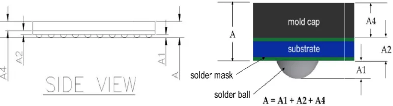
the focus of this study. Control of the package thickness needs to be tighter when the package gets thinner for applications like in mobile devices and sensors with very limited space in the thickness direction. As shown in Fig. 2, the overall package thickness A of a BGA package is composed of the solder ball collapse height A1, substrate thickness A2 and epoxy mold cap thickness A4. To get the target overall package thickness A, the solder ball collapse height A1 needs to be identified. However, this parameter A1 is dependent on the solder ball size to be used, the solder mask opening diameter and the solder mask thickness. For finer solder ball pitch, the solder mask opening size needs to be reduced as well.
Therefore, correctly predicting the
collapse height is very important in meeting the required overall package thickness. Most studies
Fig. 1. BGA package showing the solder balls Ball grid array package (BGA) is commonly used
for devices in mobile applications. It is a based package that has solder balls for
connecting to the printed circuit board (PCB) or flexible board in a surface mount
T) process. Fig. 1 shows a BGA package used for sensors in smart
The solder balls in BGA packages are attached transfer process in which flux is used from a dipping tray and the into the deposits and the whole assembly is reflowed [1]. After reflow, the solder ball or solder sphere would collapse as it attaches to the substrate metal pad. The reflowed solder ball is commonly called solder bump. The final solder ball height after reflow is the focus of this study. Control of the package thickness needs to be tighter when the package gets thinner for applications like in mobile devices and sensors with very limited space in the thickness direction. As shown in Fig. 2, the ackage thickness A of a BGA package is composed of the solder ball collapse height A1, substrate thickness A2 and epoxy mold cap thickness A4. To get the target overall package thickness A, the solder ball collapse height A1 , this parameter A1 is dependent on the solder ball size to be used, the solder mask opening diameter and the solder mask thickness. For finer solder ball pitch, the solder mask opening size needs to be
Therefore, correctly predicting the solder ball collapse height is very important in meeting the required overall package thickness. Most studies
[2-7] used Surface Evolver software to predict the shapes of full array BGA solder joints with different solder volumes. This software i very helpful especially for resulting solder joints with complex shapes. As discussed in one previous study [3], Surface Evolver allows 3 problems to be examined by discretizing an initial surface into a set of inter-connected triangular facets and then iterating this initial surface toward a minimal energy configuration by conjugate gradient methods. It is basically an energy-based method that considers surface tension of the material, gravitational effects, and internal/external pressures. This Surfac
software is robust and quite powerful but it is not very convenient to use for semiconductor package designers whose tools are mainly solid modeling or CAD (computer aided
software like SolidWorks or Autodesk Inventor. It is also observed that solder ball shape after reflow of a BGA package is not complex and
could be estimated by some simple
approximation.
This study presents simplified techniques developed for predicting solder ball collapse height that would be very useful for package designers to use and make the design and development much faster. Aside from being necessary in meeting the overall package thickness requirement even during the design stage, accurate prediction of solder ball collapse height is also very important as it
several studies [8-13] that solder joint shape and height have significant effect on solder joint reliability or fatigue life. The accuracy of any solder joint reliability modeling would be dependent on the accuracy of the solder joint shape and height estimation.
Fig. 1. BGA package showing the solder balls
7] used Surface Evolver software to predict the shapes of full array BGA solder joints with different solder volumes. This software is very helpful especially for resulting solder joints with complex shapes. As discussed in one previous study [3], Surface Evolver allows 3-D problems to be examined by discretizing an initial connected triangular n iterating this initial surface toward a minimal energy configuration by conjugate gradient methods. It is basically an based method that considers surface tension of the material, gravitational effects, and internal/external pressures. This Surface Evolver software is robust and quite powerful but it is not very convenient to use for semiconductor package designers whose tools are mainly solid modeling or CAD (computer aided-design) software like SolidWorks or Autodesk Inventor. It that solder ball shape after reflow of a BGA package is not complex and
could be estimated by some simple
2. SOLDER BALL COLLAPSE ESTIMATION
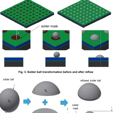
When the solder ball is reflowed after being placed on the substrate metal pad, the shape is basically transformed from a sphere to a hemispherical cap and a cylindrical volume within the solder mask thickness, t. This happens when the solder melts during reflow and fills the circular metal pad area as shown in Fi
study, a solder mask defined (SMD)
considered. For SMD substrate pad, the pad size is defined by the solder mask opening diameter. The solder mask opening exposes the metal pad on which the solder ball would be reflowed.
2.1 Theoretical Technique
Since the solder ball is just transformed to a different shape during ball attach and reflow, conservation of mass is considered. For solder material, the volume of the original solder ball (sphere) would be equal to the volume of the reflowed solder ball with a certain collapse height. This is illustrated in Fig. 4. In the study, the volume of the reflowed solder ball was simplified as the sum of volume of the
hemispherical cap, Vs, and the cylindrical
volume, Vc.
The original solder volume, V0, is given by the
formula below:
Fig. 5 shows details of a hemispherical cap from which the volume estimation of one portion of the reflowed solder was derived. This spherical cap
volume, Vs, could be calculated using the
formula:
Fig. 2. Package thickness
SOLDER BALL COLLAPSE HEIGHT
When the solder ball is reflowed after being substrate metal pad, the shape is basically transformed from a sphere to a hemispherical cap and a cylindrical volume within the solder mask thickness, t. This happens when the solder melts during reflow and fills the circular metal pad area as shown in Fig. 3. In this (SMD) pad is considered. For SMD substrate pad, the pad size is defined by the solder mask opening diameter. The solder mask opening exposes the metal pad on which the solder ball would be reflowed.
Since the solder ball is just transformed to a different shape during ball attach and reflow, conservation of mass is considered. For solder material, the volume of the original solder ball (sphere) would be equal to the volume of the d solder ball with a certain collapse height. This is illustrated in Fig. 4. In the study, the volume of the reflowed solder ball was simplified as the sum of volume of the , and the cylindrical
, is given by the
(1)
Fig. 5 shows details of a hemispherical cap from which the volume estimation of one portion of the reflowed solder was derived. This spherical cap , could be calculated using the
(2)
The other portion of the reflowed solder volume is shown in Fig. 6 and this cylindrical volume, could be calculated with the formula shown below:
The volume of the original solder ball is dependent only on the solder ball size or diameter, d0. On the other hand, the volume of
the reflowed solder ball is dependent on the solder mask thickness t, solder mask opening diameter d, and solder ball collapse height value of in Fig. 5 is equal to half of the solder mask opening diameter d.
Using the solver macro of Microsoft Excel and selecting the “GRG Nonlinear” solving method, the value of the reflowed solder ball collap
height h was determined by minimizing the
difference between the original solder ball volume and the reflowed solder ball, where the difference is given by the equation below:
= − ( + )
The solution method is basically an iter process to find the value of the solder ball
collapse height given the other known
parameters. In situations where the target solder ball collapse height h is given, then the same process is also applicable to find the correct solder ball size to be used.
2.2 Solid Modeling Technique
Semiconductor package designers are usually using solid modeling or CAD (computer design) software like SolidWorks and Autodesk Inventor to create 3-D package designs. CAD software enables the designer to see the designed part as if it were real. The solid model The other portion of the reflowed solder volume is shown in Fig. 6 and this cylindrical volume, Vc,
could be calculated with the formula shown
(3)
The volume of the original solder ball is dependent only on the solder ball size or . On the other hand, the volume of the reflowed solder ball is dependent on the , solder mask opening , and solder ball collapse height h. The in Fig. 5 is equal to half of the solder
Using the solver macro of Microsoft Excel and selecting the “GRG Nonlinear” solving method, the value of the reflowed solder ball collapse was determined by minimizing the difference between the original solder ball volume and the reflowed solder ball, where the difference is given by the equation below:
(4)
The solution method is basically an iterative process to find the value of the solder ball
collapse height given the other known
parameters. In situations where the target solder is given, then the same process is also applicable to find the correct
Solid Modeling Technique
Fig. 3. Solder ball transformation before and after reflow
Fig. 4. Original solder ball to a reflowed solder ball
can be rotated or viewed in different directions and helps the designer identify any problem with the design that needs to be corrected before actual manufacturing. Solid models created could also be directly used for any package stress or deformation analysis to make sure the packag structure is robust.
CAD software has the capability of determining the volume of any solid model created even how complex the shape is. When package designs
Fig. 3. Solder ball transformation before and after reflow
Fig. 4. Original solder ball to a reflowed solder ball
different directions and helps the designer identify any problem with the design that needs to be corrected before actual manufacturing. Solid models created could also be directly used for any package stress or deformation analysis to make sure the package
CAD software has the capability of determining the volume of any solid model created even how complex the shape is. When package designs
solder ball as a separate part would make the evaluation of the reflowed solder ball volume easy. In this study, Autodesk Inventor was used to create the solid model parts.
Fig. 5. Hemispherical cap
Fig. 6. Cylindrical volume
Fig. 7. Volume of the original solder ball determined using solid modeling software solder ball as a separate part would make the
evaluation of the reflowed solder ball volume asy. In this study, Autodesk Inventor was used
Fig. 5. Hemispherical cap
Fig. 6. Cylindrical volume
3. RESULTS AND DISCUSSION
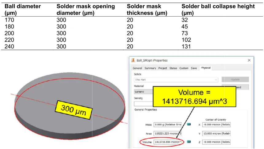
For the specific BGA package considered, the requirement from customer was to maintain the solder mask opening diameter at 300
solder mask thickness at 20 µm. The required solder ball collapse height was around 100 Different solder ball sizes were considered based on standard sizes and availability. For the theoretical calculation, the initial condition for the solder ball height was set at an arbitrary value. Different initial values were also tried and when Excel’s solver macro performed the it process, it was still able to converge to the correct solution even when initial setting was not close to the final solution. There was no issue in terms of solution convergence. The initial setting could also be based on prior experience or using preliminary CAD estimation.
With the theoretical technique applied, the results are now summarized in Table 1. It shows that using 220 µm solder ball would produce 102 µm solder ball collapse height. From this, it was then decided to use the available solder ball with µm diameter.
With solid modeling technique, the volume of the solid model part was easily determined as shown in Fig. 7 for the solder ball before reflow. The solid model shown (sphere) is having a diameter equal to 220 µm.
Fig. 8 shows the solid model of the cylindrical volume of the reflowed solder ball. It has 300 diameter, which is also the same as the solder mask opening. The thickness is 20 µm and this is the same as the solder mask thickness.
7. Volume of the original solder ball determined using solid modeling software
SSION
For the specific BGA package considered, the requirement from customer was to maintain the solder mask opening diameter at 300 µm and . The required solder ball collapse height was around 100 µm. re considered based on standard sizes and availability. For the theoretical calculation, the initial condition for the solder ball height was set at an arbitrary value. Different initial values were also tried and when Excel’s solver macro performed the iterative process, it was still able to converge to the correct solution even when initial setting was not close to the final solution. There was no issue in terms of solution convergence. The initial setting could also be based on prior experience or using
With the theoretical technique applied, the results are now summarized in Table 1. It shows that µm solder ball would produce 102 µm solder ball collapse height. From this, it was then lder ball with 220
With solid modeling technique, the volume of the solid model part was easily determined as shown in Fig. 7 for the solder ball before reflow. The solid model shown (sphere) is having a diameter
s the solid model of the cylindrical volume of the reflowed solder ball. It has 300 µm diameter, which is also the same as the solder mask opening. The thickness is 20 µm and this is the same as the solder mask thickness.
After evaluating the volume of the original solder ball and the cylindrical volume of the portion of the reflowed solder ball, the hemispherical cap solid model was adjusted so that the volume of the original solder ball would be equal to the volume of the reflowed solder ball. Fig. 9 shows that the final solder ball collapse height determined from the solid model is 102 Results show that theoretical calculation yields the same result as the solid modeling approach.
To validate the techniques developed, actual solder ball collapse height measurements were compared with estimation. Actual results were
Table 1. Summary of
Ball diameter (µm)
Solder mask opening diameter (µm)
170 180 200 220 240
300 300 300 300 300
Fig. 8. Volume of the reflowed solder ball w
Fig. 9. Volume of the hemispherical cap port After evaluating the volume of the original solder
ball and the cylindrical volume of the portion of the reflowed solder ball, the hemispherical cap d model was adjusted so that the volume of the original solder ball would be equal to the volume of the reflowed solder ball. Fig. 9 shows that the final solder ball collapse height determined from the solid model is 102 µm. alculation yields the same result as the solid modeling approach.
To validate the techniques developed, actual solder ball collapse height measurements were compared with estimation. Actual results were
analyzed using Minitab, a statistical analysis software. The actual data distribution is shown in Fig. 10. As we can see, the mean value of the solder ball collapse height is 100 µm. This is very close to the estimation obtained by the theoretical and solid modeling techniques.
Fig. 11 shows the actual image of the reflowed solder. The final solder shape is very similar to the solid model simplified approximation created using CAD software. The estimation of solder ball collapse height was also confirmed with the measurements done on this actual BGA package as shown.
Summary of solder ball collapse height calculation results
mask opening (µm)
Solder mask thickness (µm)
Solder ball collapse height (µm)
20 20 20 20 20
32 45 73 102 131
Fig. 8. Volume of the reflowed solder ball within the solder mask thickness
Fig. 9. Volume of the hemispherical cap portion of the reflowed solder ball
analyzed using Minitab, a statistical analysis are. The actual data distribution is shown in Fig. 10. As we can see, the mean value of the µm. This is very close to the estimation obtained by the theoretical and solid modeling techniques.
ge of the reflowed solder. The final solder shape is very similar to the solid model simplified approximation created using CAD software. The estimation of solder ball collapse height was also confirmed with the measurements done on this actual BGA package
ball collapse height
ithin the solder mask thickness
Fig. 10. Actual solder ball collapse height
Fig. 11. Package side view showing the solder ball collapse height measured in this study
4. CONCLUSION
Based on the actual solder ball collapse height
measurements, the theoretical and solid
modeling techniques explored here were able to give quite accurate results for the specific BGA package analyzed. Solder ball collapse height
Fig. 10. Actual solder ball collapse height measurements
Fig. 11. Package side view showing the solder ball collapse height measured in this study
Based on the actual solder ball collapse height
measurements, the theoretical and solid
modeling techniques explored here were able to give quite accurate results for the specific BGA package analyzed. Solder ball collapse height
estimations were very close to the actual measurements. Simple use of Microsoft Excel and solid modeling software readily available to package designers would be able to provide quick estimation of the solder ball collapse height and is very useful in assessing design options to meet the target overall package thickness for Fig. 11. Package side view showing the solder ball collapse height measured in this study
semiconductor BGA packages. The estimation techniques presented would also be very useful for exploring different BGA package design options like reduction in solder mask opening size especially for BGAs requiring finer solder ball pitch, reduction in solder mask thickness, and other package design adjustments based on available solder ball size.
ACKNOWLEDGEMENTS
The author would like to acknowledge the support of ST-Calamba assembly operations in the actual package assembly especially the ball attach process.
COMPETING INTERESTS
Author has declared that no competing interests exist. The products used for this research are commonly and predominantly use products in our area of research and country. There is absolutely no conflict of interest between the authors and producers of the products because we do not intend to use these products as an avenue for any litigation but for the advancement of knowledge. Also, the research was not funded by the producing company rather it was funded by personal efforts of the authors.
REFERENCES
1. Indium corporation. Variables of pin
transfer. Application Note; 2008. Available: https://www.indium.com
2. Tian YH, Wang CQ. Shape prediction and
reliability design of ball grid array solder joints. Key Engineering Materials. 2007; 2944-2947.
3. Chiang KN, Yuan CA. An overview of
solder bump shape prediction algorithms with validations. IEEE Transaction on Advanced Packaging; 2001.
4. Zheng JO. Equilibrium configurations of
oxygen bubbles on surfaces for
applications in nanostructured hematite
electrodes. Thesis submitted to
Massachusetts Institute of Technology; 2015.
5. Lin HC, Kung C, Chen RS. Evaluations of the BGA solder ball shape by using energy method. Tech Science Press; 2007.
6. Josell D, Wallace WE, Warren JA, Wheeler
D, Powell IV AC. Misaligned flip-chip solder joints: Prediction and experimental
determination of force-displacement
curves. Journal of Electronic Packaging; 2002.
7. Lim SF, Nurulakmal MS. Wetting
characterization of flip chip’s lead-free solder interconnect using surface Evolver. Journal of Physics; 2018.
8. Liu X, Lu G. Effects of solder joint shape and height on thermal fatigue lifetime. IEEE transactions on components and packaging technologies. 2003;26(2):455-465.
9. Ogunsemi B, Ikubanni P, Adediran A,
Agboola O. Effect of stand‑off height on the shear strength of ball grid array solder joints under varying pad sizes. SN Applied Sciences; 2018.
10. Njoku JE, Mallik S, Bhatti R, Emeka HA, Ekere NN. Effect of component standoff height on thermo-mechanical reliability of Ball Grid Array (BGA) solder joints operating in high-temperature ambient. IEEE 38th International Spring Seminar on Electronics Technology. 2015;231–236.
11. Lau CS, Abdullah MZ, Mujeebu MA, Yusop
NMD. Finite element analysis on the effect of solder joint geometry for the reliability of ball grid array assembly with flexible and rigid PCBs. Journal of Engineering Science and Technology. 2014;9(1):47-63.
12. Che FX, Pang JHL. Fatigue reliability
analysis of Sn–Ag–Cu solder joints subject to thermal cycling. IEEE Transactions on Device and Materials Reliability. 2013; 13(1).
13. Choubey A, Ghaffarian R. FEA and
analysis for BGA/CGA assemblies under thermal cycling. Proceedings of SMTA International; 2016.
© 2019 Talledo; This is an Open Access article distributed under the terms of the Creative Commons Attribution License (http://creativecommons.org/licenses/by/4.0), which permits unrestricted use, distribution, and reproduction in any medium, provided the original work is properly cited.
Peer-review history: