O R I G I N A L A R T I C L E
Effect of Surface Roughness in Micro-nano Scale on Slotted
Waveguide Arrays in Ku-band
Na LI1•Peng LI1 •Liwei SONG1
Received: 6 May 2016 / Revised: 7 February 2017 / Accepted: 2 April 2017 / Published online: 12 April 2017
ÓThe Author(s) 2017. This article is an open access publication
Abstract Modeling of the roughness in micro-nano scale and its influence have not been fully investigated, however the roughness will cause amplitude and phase errors of the radiating slot, and decrease the precision and efficiency of the SWA in Ku-band. Firstly, the roughness is simulated using the electromechanical coupled(EC) model. The relationship between roughness and the antenna’s radiation properties is obtained. For verification, an antenna proto-type is manufactured and tested, and the simulation method is introduced. According to the prototype, a contrasting experiment dealing with the flatness of the radiating plane is conducted to test the simulation method. The advantage of the EC model is validated by comparisons of the EC model and two classical roughness models (sine wave and fractal function), which shows that the EC model gives a more accurate description model for roughness, the maxi-mum error is 13%. The existence of roughness strongly broadens the beamwidth and raises the side-lobe level of SWA, which is 1.2 times greater than the ideal antenna. In addition, effect of the EC model’s evaluation indices is investigated, the most affected scale of the roughness is found, which is 1/10 of the working wavelength. The proposed research provides the instruction for antenna designing and manufacturing.
Keywords Slotted waveguide arraysRoughness model Micro/nano-scaleAmplitude and phase errorsRadiation characteristics
1 Introduction
A Slotted Waveguide Array(SWA) antenna has the unique advantages of having a compact configuration, stable me-chanical characteristics, low loss and high-efficiency, and is consequently widely used in communication systems. However, any structural deficiencies present, such as the surface error on slots and planes [1, 2], have a direct influence on its electrical properties. Although the surface error can be reduced to its limit value by machining the surface as flat as possible, roughness on a micro/nano-scale is inevitable [3–5]. Since a major functionality requirement is that the antenna is expected to operate at high frequen-cies such as the Ku band, the amplitude of roughness is equivalent to the working wavelength. In this case, roughness will result in amplitude and phase errors of radiating slots, and affect the self-admittance, coupling relationship, and the matching condition of slots, which can adversely affect the antenna’s electrical properties [6,7]. Since this type of antennas is currently developed for high-frequency bands, high gain, low side-lobe level, high per-formance, ultra-wide band and high precision, the influence of roughness on SWA is becoming a hot topic for research. Because the electrical performance of a SWA is directly affected by the degradation of its structural characteristics, some researchers have explored different structural factors that influence the antenna’s electrical properties. In terms of general array antennas, the prime interest has been on determinations of the pointing gain loss. On this subject, RUZE [8] published the first work related to this field and Supported by National Natural Science Foundation of China (Grant
Nos. 51305322, 51405364, 51475348). & Peng LI
1 Key Laboratory of Electronic Equipment Structure Design of Ministry of Education, Xidian University, Xi’an 710071, China
pursued issues regarding the effect of the position and amplitude-phase errors of radiating elements on the antenna gain loss. HSIAO [9] extrapolated that the effect formula of error on the beam’s width, which provided a very beneficial and applicable supplement to extant theo-ries on antenna gain loss. Subsequently, WANG [10] investigated the influence of random errors for each radi-ating element on the performance of a phased array antenna based on the probability method. However, both RUZE and WANG assumed that the structural error was within a priori determined distribution and failed to analyze prac-tical structural deficiencies through a finite element anal-ysis of the antenna structure. Recently, TAKAHASHI, et al. [11], and SONG, et al. [12], investigated the dynamics related to distortions of the radiating surfaces and their impact on the antenna’s electrical performance. However, the majority of research concentrated on the relation between radiating slot information and the elec-trical performance of the antenna, and an extensive number of research papers has been published on this topic. Research has also been conducted on the relationship between radiating slot information and cavity errors, but no concrete associations have yet been determined. Moreover, the roughness of the inner wall of the radiating waveguide has hardly been studied.
Through his modeling research on the roughness of the waveguide, MORGAN [13] obtained a result which is now considered classical. The following analyses are found to be consistent with MORGAN’s results [14–16]. However, in MORGAN’s and the other analyses, some periodic functions were used. In the other hand, TSANG, et al. [17], used a random function to simulate roughness, which was charac-terized using the root mean square(RMS), correlation length, and the correlation function. Certainly, an advantage of using a random model was that it allows a similar approach as in the case of roughness occurring in copper intercon-nects. LUKIC and FILIPOVIC [18] modeled a rectangular-coaxial roughness by investigating the cubical, semi-ellip-soidal and pyramidal indentation, and his results showed that roughness accounted for up to 9.2% of their overall loss for frequencies below 40 GHz. Nonetheless, the roughness on the radiating waveguide is neither totally random nor clearly deterministic, and the altitude distribution, the slope and curve of the random model are associated with resolution and sampling length of the measuring instrument, while it is not unique [19–21]. Fractal geometry has provided an additional means of description and roughness analysis [22–24]. In our previous works, a one-dimensional fractal analysis of roughness is investigated [25], but the scope of its applicability is limited, because it is based on a deter-ministic mathematical form.
Based on previous studies, this paper seeks to investi-gate the relationship between surface roughness and
antenna electrical properties. For this reason, an EC model was used to simulate roughness, based on which an influ-ence mechanism equation was deduced.
2 Roughness Model
2.1 Electromechanical Coupled Roughness Model
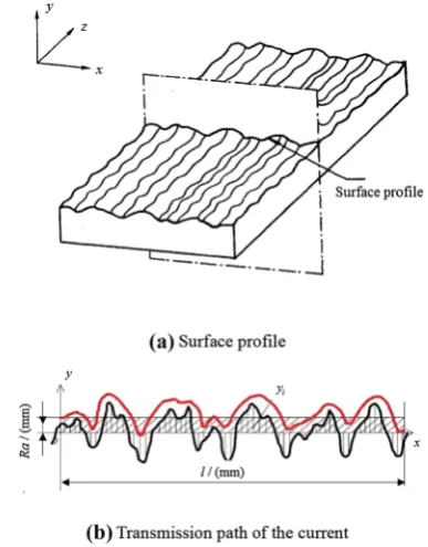
In the mechanical field, roughness is the surface profile of an object separated from its surrounding environment, which is the intersection transversal between the vertical plane and actual surface, as shown in Fig. 1(a). However, on the inner wall of a waveguide, the transmission path of the electromagnetic wave is not completely consistent with the surface profile. Even though roughness (black line in Fig.1(b)), may be bigger or smaller relative to the working wavelength of the waveguide, the surface profile has little influence on the transmission path (red line in Fig.1(b)) [26]. Therefore, an effective model should be built according to the most influential surface profile, and profile elements that are too big or too small should be considered as sources producing noise and this noise should be filtered out. Since roughness is a basic mechanical parameter, while filtering concerns is the electrical properties, the proposed novel roughness modeling method can be called the electromechanical coupled roughness model and abbreviated as the EC model.
In order to model roughness, a Monte Carlo simulation was first used [27]. Since two dimensional roughness
exhibits waviness in both directions, if we denote the root mean square (RMS) value of roughness as Ra, then the power spectral density function of the fractal function is [28]
Sðwx;wyÞ ¼ G2ðD1Þ .
ð2 lnðcxcyÞ ðwxwyÞð 52DÞÞ
h i
; ð1Þ
whereDis the fractal dimension, andGis the characteristic length,cx¼1=Lx,cy¼1
Ly, whereLxandLyare the
sam-pling lengths of roughness in thexand y directions, whilewx
andwyare the frequencies of the roughness in thexandy
directions, respectively. If the power spectral density func-tions in each direction areS(wx) andS(wy), respectively, and
Ra/GD1, then Eq. (1) can be expressed as
Sðwx;wyÞ ¼
1
Ra2SðwxÞSðwyÞ: ð2Þ
We performed a uniform discretization of roughness, where the numbers of discrete points in each direction are M andN, the corresponding separation distances of adja-cent points areDxandDy, whereDx¼Lx=M,Dy¼Ly
N, and the height of each data points on the surface is given by
fðxm;ynÞ ¼
1 LxLy
XM=2
ðmk¼1M=2Þ
XN=2
ðnk¼1N=2Þ
Fðkmk;knkÞ
expðiðkmkxmþknkynÞÞ;
ð3Þ
where xm¼mDx;yn¼nDy, m¼1M=2*M=2,
n¼1N=2*N=2, whileFðkmk;knkÞis given by
Fðkmk;knkÞ ¼2p
ffiffiffiffiffiffiffiffiffiffiffiffiffiffiffiffiffiffiffiffiffiffiffiffiffiffiffiffiffiffi
LxLySðkmk;knkÞ q
; ð4Þ
wherekmk¼2pmk=Lxandknk¼2pnk
Ly.
For fðxm;ynÞ to be real, Fðkmk;knkÞ should satisfy the
relationship:
Fðkmk;knkÞ ¼Fðkmk;knkÞ; Fðkmk;knkÞ
¼Fðkmk;knkÞ;
whereFðÞ is the Fourier transformation. Therefore, the roughness modelfðx;yÞcan be expressed as
fðx;yÞ ¼ 1
Ra2fðxÞfðyÞ; ð5Þ
and the one dimension roughness model are
fðxÞ ¼GD1X
1
n¼1
cosð2pcnxþu nÞ
cð2DÞn ; ð6Þ
fðyÞ ¼GD1X
1
m¼1
cosð2pcmyþu mÞ
cð2DÞm : ð7Þ
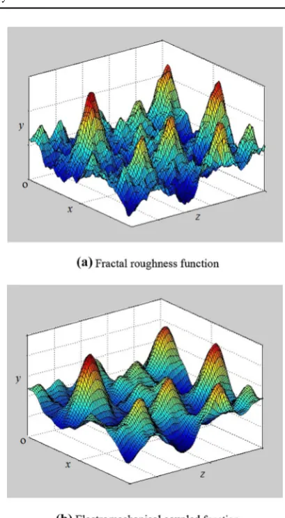
As shown in Fig.2(a), a two-dimensional Weierstrass-Mandelbrot (W-M) fractal function was used as the basic model to describe the surface profile as comprehensively as
possible [21]. Then, the effective roughness profile was determined based on the transmission path, and the filter function’s upper and lower limits were chosen. Finally, the EC model was built as shown in Fig.2(b). The specific modeling parameters were detailed and illustrated in sub-sequent equations. A two-dimensional Gaussian was used as the filter function:
hðx;yÞ ¼ 1
A2kxkyexp pðx=AkcxÞ 2
pyAkcy2
h i
; ð8Þ
wherekxandkyare the working wavelengths in thexandy directions, while kcx, kcy and A are the truncation wave-lengths and width coefficient of the filter, respectively.
According to the electrical characteristics of the antenna, 94% of the surface current was distributed within 3 times the skin depth, so the upper and lower limits of the filter are
kmax¼2 ffiffiffiffiffiffiffiffiffiffiffiffiffiffiffiffiffiffiffiffiffi1=ðpfl0rÞ p
; ð9Þ
kmin¼kmax=3; ð10Þ
thefis the current frequency of the waveguide, andl0and rare the permeability and conductivity of the waveguide’s inner wall, respectively.
The basic model given in Eq. (5) can be divided into two parts as
fðx;yÞ ¼f1ðx;yÞ þf2ðx;yÞ; ð11Þ
wheref(x,y) is the basic model, which is composed of two parts: f1(x, y) is the representationof noise in the surface profile, which has little influence on the transmission path of electromagnetic wave, andf2(x,y) is the effective profile data, which is just the EC roughness model. Usingf1(x,y) as the assessment base level:
f1ðx;yÞ ¼fðx;yÞ hðx;yÞ
¼
Z 1
1
Z 1
1
fðn;gÞh xð n;ygÞdndg: ð12Þ
The EC model becomes: f2ðx;yÞ ¼fðx;yÞ f1ðx;yÞ
¼fðx;yÞ
Z 1
1
Z 1
1
fðn;gÞh xð n;ygÞdndg:
ð13Þ
If the measured data are discrete, the assessment base levelf1
i;j becomes
fi1;j¼ X
M
k¼M XN
l¼N
zik;jlhk;lDxDy; ð14Þ
where i¼M; ;LXM; j¼N; ;LYN, hk;l¼ 1
a2kcxkcyexp pðkDx=akcxÞ 2
plDyakcy2
h i
. The EC modelf2
i;jis
fi2;j¼fi;jfi1;j¼fi;j XM
k¼M XN
l¼N
fik;jlhk;lDxDy: ð15Þ
2.2 Evaluation indices of the EC roughness model
Traditional definitions of the surface roughness usually contain only local and one-dimensional information, and the arithmetical mean error Rais regarded as the unique evaluation indices [29]. The features of two or three dimensional roughness cannot be fully represented by this conventional index. Moreover, Ra is a non-deterministic index, which means that different roughness contours processed by different technologies may yield the sameRa. For the fractal geometric model, two parameters(DandG) are introduced to describe roughness characteristics. Index Dis the dimension parameter, whileGis the fundamental frequency in space and represents roughness density. Although these two indexes allow more accurate roughness
quantification, they cannot be adequately measured directly and it is hard to relate them to the measured parameters of roughness. For these reasons, the applicability of the fractal model is limited. Studies have shown that the main dif-ferences between roughness contours processed by differ-ent technologiesbut with the same Raare the density and regularity of peaks and valleys. The information appears as the expansion length of the roughness profile, which is the principal reason for changing of the transmission path. Therefore, two parameters,RaandRlare introduced as the roughness model indexes.Rais the main parameter, and its value is equal to the arithmetical mean deviation;Rlis the auxiliary parameter, and its value is the length of effective roughness contour. The equations for these two indices are
Rað Þ ¼1 1 lx
Z lx
0
fðxÞ j jdx1
n
Xn
i¼1
yi
j j;
Rlð Þ ¼1 1 lx
Z lx
0
ffiffiffiffiffiffiffiffiffiffiffiffiffiffiffiffiffiffiffi
1þf02ðxÞ q
dx
1 lx
Xn1
i¼1
ffiffiffiffiffiffiffiffiffiffiffiffiffiffiffiffiffiffiffiffiffiffiffiffiffiffiffiffiffiffiffiffiffiffiffiffiffiffiffiffiffiffiffiffiffiffiffiffiffiffiffi
ðxiþ1xiÞ 2
þ ðyiþ1yiÞ 2 q ; 8 > > > > > > > > > < > > > > > > > > > : ð16Þ
where lx and f(x) are the sampling length and roughness
model in the x direction, while the (xi, yi) is a discrete
measured datumof roughness.
Using the two-dimensional roughness indices as the description model can not only reflect the relief intensity but also the fluctuationgradientfor roughness, which required for both mechanical and electromagnetic field analyses. Even though using a calculation based on a one-dimensional model displays a clear mathematical principle and its simple structural equation is easily calculated, it is revealed to be inadequate since the electromagnetic field dispersed over the waveguide inevitably demonstrates some directional properties. Furthermore, the real surface roughness is anisotropic and should be considered simul-taneously from the length wise and transverse directions. Thus, [Ra(2),Rl(2)] for the two-dimensional EC model are formulated as follows:
Rað Þ ¼2 1 lxly
Z lx
0 Z ly
0
fðx;yÞ j jdxdy;
Rlð Þ ¼2 1 lxly
Z lx
0 Z ly
0
ffiffiffiffiffiffiffiffiffiffiffiffiffiffiffiffiffiffiffiffiffiffiffiffiffiffiffiffiffiffiffiffiffiffiffiffiffiffiffi
1þ of ox 2 þ of oy 2 s dxdy: 8 > > > > < > > > > : ð17Þ
3 Factors Affecting Roughness
antenna working in the GHz range, roughness of the waveguide becomes a critical reason for position and directional offset of the radiation slot. Therefore, in order to establish a connection between the roughness and radi-ating slot error, the key difficulty lies in antenna error analysis. Based on the model f(x, y), the roughness infor-mation should be primarily represented using antenna coordinates [30].
Given a point on the roughness surfaceA(xA,yA,zA) and
an anglea, an elliptical curve can be obtained using a line drawn through the pointA, whose axis is the origin andais the angle. Let the center of this ellipse beQ(xQ,yQ,zQ) and
an intersection point of the axis and the ellipse be denoted by S(xS, yS, zS). Thus, an area corresponding to the
roughness coordinatedðxd
n; ydn; zdnÞis established, where the
pointQis its origin and the elliptical surface is on thexdnoydn plane. If the antenna coordinate is (x, y, z), the transfor-mation process needs to be shifted twice and rotated as follows:
x0
y0
z0þzQ 0 @
1
A¼
1 0 0
0 cosxx sinxx
0 sinxx cosxx 0 @ 1 A x d n yd n zd n 0 @ 1
A; ð18Þ
xþxQ
yþyQ
z
0 @
1
A¼
cosxz sinxz 0 sinxz cosxz 0
0 0 1
0 @
1 A xy00
z0 0 @
1
A; ð19Þ
where xx¼p=2x0x, and x0x can be deduced by tanx0x¼
cosbþcosa
sinb , while (x0, y0, z0) is the inter mediate coordinate during the transformation process.
If the roughness model is zd
nðxdn;ydnÞ, then according to
Eqs. (18), (19), the slot error characteristics are
D~rn¼
ffiffiffiffiffiffiffiffiffiffiffiffiffiffiffiffiffiffiffiffiffiffiffiffi
x2þy2þz2 p
ffiffiffiffiffiffiffiffiffiffiffiffiffiffiffiffiffiffiffiffiffiffiffiffiffiffiffiffiffix2d n þy2ndþz2nd q ; ð20Þ
fhn¼ arccosðz=xÞ arccosðzdn
xdnÞ
; ð21Þ
fun¼ arctanðy=xÞ arctanðydn
xdnÞ
: ð22Þ
If the excitation current of unitnisIn, its coordinate are
(xn,yn,zn), andInis symmetrical on two coordinate axes,
the radiation field intensity of the antenna on the plane (u¼u0) is [31]
E0ðh;u0Þ ¼ X
n
Inexp j½kðxndxcosu0þyndysinu0Þ
ðsinhsinh0Þ
, X
n
In;
ð23Þ
whereE0ðh;u0Þ is the far field pattern, h; u are the
azi-muth in the far field,dxanddyare the distances of the array
element, xn andynare the position coordinates of unit n,
andkis the transfer constant. When the position error of
unitnisðxd
n;ydn;zdnÞ, the radiation field intensity becomes as
follows:
E0ðh;uÞ ¼ X
n
Jnexpj½kððxnþxdnÞdxcosu0þ
ðynþydnÞdysinu0Þðsinhsinh0Þ ,
X
n
Jn; ð24Þ
where
Jn ¼Inexp j½kðxdndxcosðuþnunÞþ
ydndysinðuþnunÞÞsinðhþnhnÞ þkzdndzcosðhþnhnÞ:
4 Testing of Proposed Methods
4.1 Experiment on a planar slot antenna
In order to provide evidence supporting the EC roughness model and how factors related to its influence antenna performance, a miniature planar slot array antenna was processed as an experimental project case. The antenna operated in the Ku band, with a central frequency of 12 GHz, a gain of no less than 17 dB, and the first lobe level was no higher than -16 dB. Its structural dimensions were 150 mm9126 mm, and it had ten radiating waveguides and eight vertical offset slots on each waveguide.
Roughness on the inner wall of the radiating waveguides was measured using the Taylor Hobson profile measuring instrument. Indexes Ra and Rl of the measurement data [Ra1, Rl1] and the EC roughness model [Ra2, Rl2] were calculated as follows:
Ra1¼1 lx
Z lx
0
zðxÞ
j jdx; ð25Þ
Ra2\2G
D1
p
cðD2Þn
1cD2; Ra
2 /GD1; ð26Þ
Rl1¼
ffiffiffiffiffiffiffiffiffiffiffiffiffiffiffiffiffiffiffiffiffiffiffi
1 m
Xm
i¼1
fðxiÞ 2 s
; ð27Þ
Rl2¼
Z w2
w1
SðwÞdx¼ G
ðD1Þ
wð2DÞ½2 lncð42DÞ1=2: ð28Þ
for S3 it is 0.703 mm, with a maximum error of 13%, which demonstrates the accuracy of the EC model.
The antenna was fixed on the test turning platform to ensure that the radiating plane was parallel to the direction of gravity and the scanning plane of the measuring waveguide probe. The near-field data of the antenna was measured by the plane near-field scanning method, while the far-field data were obtained through the near-field to far-fieldtransformation(nffft) method [32,33]. The plotting radiating pattern is for the H-plane. The electrical perfor-mance was evaluated using the antenna gain, the maxi-mumsidelobe level, and the 3-dB beamwidth on azimuth plane, as well as the maximum sidelobe level, and 3-dB beamwidth on the pitch plane.
4.2 Simulation of the SWA with Roughness
High-precision characteristics of SWA result in high costs and a long manufacturing cycle. Thus, manufacturing antennas in large quantities for experimental reasons is difficult and even impractical. Therefore, antenna simula-tion analysis is gaining increasing attensimula-tion and interest from the scientific and industrial community, because of repeatability and low cost. However, the key to accurate simulations is to incorporate surface roughness in the numerical model. Only a small number of existing com-mercial software can accurately analyze the antenna taking roughness into account, and the structural and electro-magnetic analyses are usually carried out separately, which will cause a mismatch in structural and electromagnetic meshes. In order to deal with these issues, the grid con-version and roughness data adding methods are presented in this paper. As shown in Fig.3, the simulation was conducted as follows:
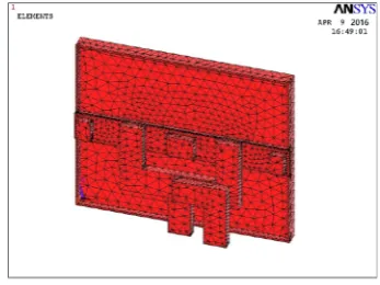
First, the finite element model of the antenna was con-structed using ANSYS 11.0, as shown in Fig.4. The number of nodes was 19263, while there were 55169 units. The material chosen was Al-6063, with a modulus of elasticity of 70 GPa, a Poisson ratio of 0.33, and a density of 2.79103(kgm-3).
The second step was to add the roughness information to the ideal antenna model. The structural boundary of the antenna was determined by the shape of the data stream, and the roughness model was added into it as an additional
boundary. The finite element model of the antenna with roughness was built using the GUI.
The third step was to translate the structural model to an electromagnetic analysis model by converting the tetrahe-dral body elements of the structural model into triangular surface elements, which were necessary for the electro-magnetic analysis. Based on the surface elements, a surface model of the antenna was built and the intracavity model was extracted from it. Finally, the intracavity model of the antenna was introduced into HFSS 11.0 and the electrical properties of the model were obtained.
4.3 Results and Discussion
To verify the accuracy of the proposed simulation method, a flatness comparison of the radiating plane was made between the simulation results and the test data, as shown in Fig.5, where the series of radiating slots forms the
Table 1 Comparison of two indexes of measurement data and EC model
Methods Indexes Region S1 Region S2 Region S3 Measurement Ra/mm 0.495 1.477 0.703
Rl/mm 0.874 3.453 1.367 EC model Ra/mm 0.508 1.501 0.635 Rl/mm 0.970 3.415 1.248
Fig. 3 Simulation process of the antenna with roughness
abscissa and thezcomponent was the vertical coordinate. The simulation results along with the slot numbers are all highly consistent with the test data results. A small error occurs, because the simulation was based on an antenna working under ideal circumstances, which was not the case in the practical antenna test.
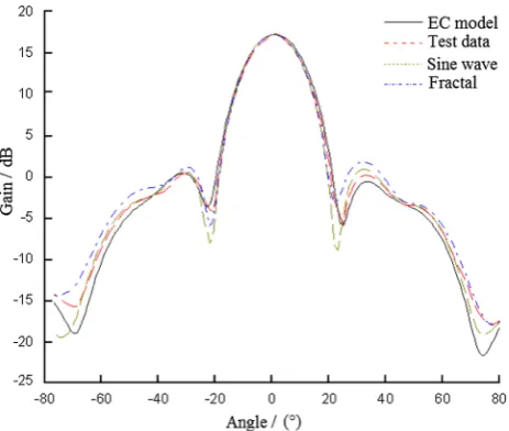
To verify the proposed roughness model, a comparison was made using the test data of the antenna pattern, where the sine wave represents the period model and the Gaussian represents the random model. As shown in Fig.6, the results of the periodic model(based on the sine wave approximation) have a lower first side-lobe than the test data, because most of the roughness information has been lost. The results obtained from the performance degrada-tion analysis of the fractal model appears more severe than
the result of the periodic models, due to the fact that the fractal model contains more roughness information, which severely changes the transmission path of the electromag-netic wave. However, it does not completely coincide with the test data, because it is built according to the actual surface profile, not the transmission path. The results of the EC model are closest to the test data, indicating that it can describe the roughness information more precisely than any of the other models can.
As shown in Fig.7, increasing the roughness indices also broadens the beam width and raises the side-lobe level of the antenna, while it had little impact on the antenna’s gain. The antenna is affected the most when the amplitude of roughness is equal to approximately one tenth of the working wavelength. Relative to Ra, Rl has a stronger influence on the first side-lobe level of the antenna. These findings suggest that the strongest influence indexes, and reducing them in the manufacturing process is an effective way to ensure the design accuracy of the antenna, which will greatly reduce the production cost and shorten the production cycle as well.
5 Conclusions
(1) An EC roughness model is presented to characterize the roughness by using the Gaussian filter. Two evaluation indices of the EC model are introduced. (2) ARelationship between the roughness and the array’s
radiation properties is obtained by analyzing the positional difference of the radiating slots.
(3) A novel simulation method for the non-ideal antenna is introduced.
Fig. 5 Flatness comparison of the simulation result to the test data
Fig. 6 Comparison of different models to the test data of the antenna pattern
(4) Existence of roughness strongly broadens the beam width and raises the side-lobe level of SWA, with the maximum value being 1.2 times greater than obtained by a smooth antenna.
(5) The most affected scale of the roughness is found, which is 1/10 of the working wavelength.
Open Access This article is distributed under the terms of the Creative Commons Attribution 4.0 International License (http://crea tivecommons.org/licenses/by/4.0/), which permits unrestricted use, distribution, and reproduction in any medium, provided you give appropriate credit to the original author(s) and the source, provide a link to the Creative Commons license, and indicate if changes were made.
References
1. CHEN X, HUANG K, XU X. A Novel planar slot array antenna with omnidirectional pattern[J].IEEE Transactions on Antennas & Propagation, 2011, 59(12): 4853–4857.
2. LIU F,XU G,LIANG L,et al. Least squares evaluations for form and profile errors of ellipse using coordinate Data[J]. Chinese Journal of Mechanical Engineering, 2016, 29(5): 1–9.
3. CHENG Z, LIAO R. Effect of surface topography on stress concentration factor[J]. Chinese Journal of Mechanical Engi-neering, 2015, 28(6): 1141–1148.
4. BARBARINO S, FABRIZIO C. Effect of the substrate permit-tivity on the features of a UWB planar slot antenna[J].Microwave & Optical Technology Letters, 2010, 52(4): 935–940.
5. HESSAINIAA Z, BELBAHA A, YALLESEA M, et al. On the prediction of surface roughness in the hard turning based on cutting parameters and tool vibrations[J]. Measurement, 2013, 46(5): 1671–1681.
6. MORINI A, ROZZI T, VENANZONI G. On the analysis of slotted waveguide arrays[J].IEEE Transactions on Antennas & Propagation, 2006, 54(7): 2016–2021.
7. MONTISCI G, MAZZARELLA G, CASULA G. A. Effective analysis of a waveguide longitudinal slot with cavity[J]. IEEE Transactions on Antennas & Propagation, 2012, 60(7): 3104–3110. 8. RUZE J. Pattern degradation of space fed phased arrays[R]. M.I.T. Lincoln Laboratory, Lexington, MA, Project report SBR-1, 1979.
9. HSIAO J. Array sidelobes, error tolerance, gain and beam-width[R]. NRL Report 8841, Interim Report Naval Research Lab., Washington, DC. Electromagnetics Branch, 1984. 10. WANG H S C. Performance of phased-array antennas with
mechanical errors[J].IEEE Transactions on Aerospace & Elec-tronic Systems, 1992, 28(2): 535–545.
11. TAKAHASHI T, NAKAMOTO N, OHTSUKA M, et al. On-board calibration methods for mechanical distortions of satellite phased array antennas[J]. IEEE Transactions on Antennas & Propagation, 2012, 60(60): 1362–1372.
12. SONG L W, DUAN B Y, ZHENG F, et al. Performance of planar slotted waveguide arrays with surface distortion[J].IEEE Trans-actions on Antennas & Propagation, 2011, 59(9): 3218–3223. 13. MORGAN P. Effect of surface roughness on eddy current losses
at microwave frequencies[J].Journal of Applied Physics, 1949, 20(4): 352–362.
14. HOLLOWAY C L, KUESTER E F. Power loss associated with conducting and superconducting rough interfaces[J]. IEEE Transactions on Microwave Theory & Techniques, 2000, 48(10): 1601–1610.
15. GU X X, TSANG L, BRAUNISCH H. Modeling effects of random rough interface on power absorption between dielectric and conductive medium in 3-D problem[J].IEEE Transactions on Microwave Theory & Techniques, 2007, 55(3): 511–517. 16. WU Z, DAVIS L E. Surface roughness effect on surface
impe-dance of superconductors[J].Journal of Applied Physics, 1994, 76(6): 3669–3672.
17. TSANG L, BRAUNISCH H, DING R. H, et al. Random rough surface effects on wave propagation in interconnects[J]. IEEE Transactions on Advanced Packaging,2010, 33(4): 839–856. 18. LUKIC M V, FILIPOVIC D S. Modeling of 3-D Surface
roughness effects with application to l-coaxial lines[J]. IEEE Transactions on Microwave Theory and Techniques, 2007, 55(3): 518–525.
19. CHEN Q, CHOI H W, WONG N. Robust simulation methodol-ogy for surface-roughness loss in interconnect and package modelings[J].IEEE Transactions on Computer-Aided Design of Integrated Circuits And Systems, 2009, 28(11): 1654–1665. 20. GUO X C, JACKSON D R, KOLEDINTSEVA M Y, et al. An
analysis of conductor surface roughness effects on signal propa-gation for stripline interconnects[J]. IEEE Transactions on Electromagnetic Compatibility,2014, 56(56): 707–714. 21. DING R H, TSANG L, BRAUNISCH H. Wave propagation in a
randomly rough parallel-plate waveguide, microwave theory and techniques[J]. IEEE Transactions on Microwave Theory & Techniques, 2009, 57(5): 1216–1223.
22. PERROTTI V, APRILE G, DEGIDI M, et al. Fractal analysis: a novel method to assess roughness organization of implant surface topography[J]. International Journal of Periodontics & Restorative Dentistry,2011, 31(6): 633–639.
23. MAJUMDAR A, BHUSHAN B. Role of fractal geometry in roughness characterization and contact mechanics of surfaces[J]. Journal of Tribology, 1990, 112(2): 205–216.
24. ZHAO H,WU Q. Application Study of fractal theory in mechanical transmission[J]. Chinese Journal of Mechanical Engineering, 2016, 29(5): 871–879.
25. LI N, ZHENG F. Effect of micro/nano-scale rough surface on power dissipation of the waveguide: model and simulate[J]. Journal of Nanoscience & Nanotechnology, 2011, 11(12): 11222–11226. 26. DING R, TSANG L, BRAUNISCH H. Random rough surface
effects in waveguides using mode matching technique and the method of moments[J].Components Packaging & Manufacturing Technology IEEE Transactions on, 2012, 2(1): 140–148. 27. ZHANG J, GUO F. Statistical modification analysis of helical
planetary gears based on response surface method and monte carlo simulation[J].Chinese Journal of Mechanical Engineering, 2015, 28(6):1194–1203.
28. JAHN R, TRUCKENBRODT H. A simple fractal analysis method of the surface roughness[J]. Journal of Materials Pro-cessing Technology, 2004, 145(1): 40–45.
29. WHITEHOUSE D J. Surfaces and their Measurement[M]. Oxford: Elsevier, Butterworth-heinemann, 2004.
30. JAMNEJAD-DAILAMI V, SAMII Y R. Some important geo-metrical features of conic-section-generated offset reflector antenna[J]. IEEE Transactions on Antennas & Propagation, 1980, 28(6): 952–957.
31. HUNG Y. Impedance of a narrow longitudinal shunt slot in a slotted waveguide array[J]. IEEE Transactions on Antennas & Propagation, 1974, 22(4): 589–592.
32. OLINER A. The impedance properties of narrow radiating slots in the broad face of rectangular waveguide: Part I —theory[J]. IEEE Transactions on Antennas & Propagation, 1957, 5(1): 4–
11.
representation on arbitrary surfaces in near-field antenna mea-surements[J]. IEEE Transactions on Antennas & Propagation. 2013, 61(4): 2025–2033.
Na LI, born in 1982, is currently a associate professor at Key Laboratory of Electronic Equipment Structure Design, Ministry of Education, Xidian University, China. She received her PHD degree fromXidian University, China, in 2012. Her research interests include surface error modeling, surface error reconstruction and the func-tionality design of the surface. Tel: ?86-029-88203040; E-mail: [email protected]
Peng LI, born in 1981, is currently a associate professor at Key Laboratory of Electronic Equipment Structure Design, Ministry of Education, Xidian University, China. His research interests include multidisciplinary design optimization of the Slotted Waveguide Array. Tel:?86-029-88203040; E-mail: [email protected]