ter Maten et al.Journal of Mathematics in Industry (2017) 7:2 DOI 10.1186/s13362-016-0025-5
E S S AY
Open Access
Nanoelectronic COupled problems
solutions - nanoCOPS: modelling, multirate,
model order reduction, uncertainty
quantification, fast fault simulation
E Jan W ter Maten
1*, Piotr A Putek
1,2, Michael Günther
1, Roland Pulch
2, Caren Tischendorf
3,
Christian Strohm
3, Wim Schoenmaker
4, Peter Meuris
4, Bart De Smedt
4, Peter Benner
5, Lihong Feng
5,
Nicodemus Banagaaya
5, Yao Yue
5, Rick Janssen
6, Jos J Dohmen
6, Bratislav Tasi´c
6, Frederik Deleu
7,
Renaud Gillon
7, Aarnout Wieers
7, Hans-Georg Brachtendorf
8, Kai Bittner
8, Tomáš Kratochvíl
9, Jiˇrí Petˇrzela
9,
Roman Sotner
9, Tomáš Götthans
9, Jiˇrí Dˇrínovský
9, Sebastian Schöps
10, David J Duque Guerra
10,
Thorben Casper
10, Herbert De Gersem
10, Ulrich Römer
10, Pascal Reynier
11, Patrice Barroul
11,
Denis Masliah
11and Benoît Rousseau
11*Correspondence:
[email protected] 1Bergische Universität Wuppertal, Gauß-Straße 20, Wuppertal, 42119, Germany
Full list of author information is available at the end of the article
Abstract
The FP7 project nanoCOPS derives new methods for simulation during development of designs of integrated products. It covers advanced simulation techniques for electromagnetics with feedback couplings to electronic circuits, heat and stress. It is inspired by interest from semiconductor industry and by a simulation tool vendor in electronic design automation. The project is on-going and the paper presents the outcomes achieved after the first half of the project duration.
Keywords: multirate; model order reduction; co-simulation; uncertainty quantification; power-MOS devices; RF-circuitry; bond wires; coupled problems; multiphysics; fault simulation
1 Introduction
Designs in nanoelectronics often lead to large-size simulation problems and include strong feedback couplings. Industry demands the provisions of variability to guarantee quality and yield. It also requires the incorporation of higher abstraction levels to allow for sys-tem simulation in order to shorten the design cycles, while at the same time preserving accuracy. The nanoCOPS FP project addresses the simulation of two technically and commercially important problem classes identified by our industrial partners (NXP Semi-conductors, ON Semiconductor, ACCO Semiconductor, and MAGWEL):
• Power-MOS devices, with applications in energy harvesting, that involve couplings between electromagnetics (EM), heat and stress, and
• RF-circuitryin wireless communication, which involves EM-circuit-heat coupling and multirate behaviour, together with analogue-digital signals.
To meet market demands, the scientific challenges are to:
ter Maten et al.Journal of Mathematics in Industry (2017) 7:2 Page 2 of 19
• create efficient and robust simulation techniques for strongly coupled systems, that exploit the different dynamics of sub-systems within multiphysics problems and that allow designers to predict reliability and ageing;
• include a variability capability such that robust design and optimization, worst case analysis, and yield estimation with tiny failure probabilities are possible (including large deviations like -sigma);
• reduce the complexity of the sub-systems while ensuring that the operational and coupling parameters can still be varied and that the reduced models offer higher abstraction models that are efficient to simulate.
Achieving solutions to these challenges has considerable industrial impact. The overall
objectiveof nanoCOPS is to advance a methodology for circuit-and-system-level mod-elling and simulation based on best practice rules to deal with coupled electromagnetic
field-circuit-heat problemsas well as coupled electro-thermal-stress problems that
emerge in nanoelectronic designs. The new methods developed are robust and allow for strong feedback coupling when integrating systems to increase the performance of both existing devices and when integrating systems to produce new devices.
First outcomes have been reported in [, ]. The project is on-going and the paper presents the outcomes achieved after the first half of the project duration. Recently, at the DATE- conference in Dresden, Germany, we gave dedicated presentations to de-signers and to engineers with backgrounds in mathematics and in electronics [–]. On the project website http://www.fp-nanocops.eu/ special videos have been made available. Here also more publications can be found. The current paper addresses mathematicians and points out how mathematics as essential ingredient for innovation is transfered for successful use in industry.
With the new techniques it is possible to efficiently analyze the effects due to variability. Our methods are designed to solve reliability questions resulting from
manufacturabil-ity. They facilitate robust design as well as enable worst case analysis. They can also be used to study effects due to ageing. Ageing causes variations in parameters over a long-term period, which cannot be predicted exactly and thus are typically uncertain. The chal-lenges for an Integrated Circuit (IC) are that each device has its own electrical and thermal conditions, which are changing over time (due to ageing, for example). Here, each device has its own required life-time.
Novel Model Order Reduction techniques, developed here for the fast repeated simula-tion of the coupled problems under considerasimula-tion, are applicable to both coupled systems and parameterized sub-systems. As such they are an essential ingredient for the Uncer-tainty Quantification.
In summary, our solutions are
• advanced co-simulation/multirate/monolithic techniques, combined with envelope/wavelet approaches;
• new generalized techniques in Uncertainty Quantification (UQ) for coupled problems, tuned to the statistical demands from manufacturability;
• enhanced, parametric Model Order Reduction techniques for coupled problems and for UQ.
ter Maten et al.Journal of Mathematics in Industry (2017) 7:2 Page 3 of 19
Table 1 Partners in nanoCOPS
Abbr. Partner
BUW Bergische Universität Wuppertal, Germany (coordinator) HUB Humboldt Unversität zu Berlin, Germany
TUD Technische Universität Darmstadt, Germany UGW Ernst-Moritz-Arndt-Universität Greifswald, Germany
FHO FH OÖ Forschungs- und Entwicklungs GmbH, Hagenberg im Mühlkreis, Upper Austria, Austria KUL Katholieke Universiteit Leuven, Belgium
BUT Vysoké u˘cení technické v Brn ˘e, Brno University of Technology, Czech Republic MPG Max Planck Institute for Dynamics of Complex Technical Systems, Magdeburg, Germany NXP NXP Semiconductors Netherland B.V., Eindhoven, The Netherlands
ONN ON Semiconductor Belgium, Oudenaarde, Belgium MAG MAGWEL NV, Leuven, Belgium
ACC ACCO Semiconductor, Louveciennes, France
measurements and supply material data as well as process data. A thorough comparison to
measurementson real devices is being made to demonstrate the industrial applicability. Our consortium brings together extensive R&D experience in nanoelectronic IC simu-lation and complementary areas of expertise. It includes seven universities, one research institute, two large-scale semiconductor companies, and two SMEs, see Table .
2 Progress and results
In this section we give an impression of outcomes achieved in the first half of the project duration. We refer with the abbreviations in Table to the various project partners.
2.1 Simulation environment
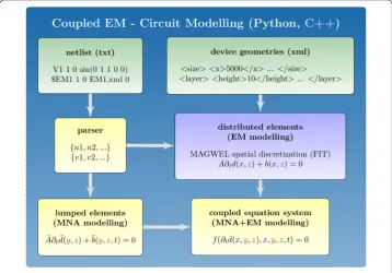
Electronic devices consist of a large number of components. Many parts are accurately described by a circuit model, whereas semiconductor parts and configurations suffering from electromagnetic interference necessitate the use of field models. The overall be-haviour of the device needs to be simulated by a field-circuit coupled method. Improve-ments on such coupled techniques indirectly lead to more reliable and better integrated devices. In order to be able to incorporate the mutual electromagnetic influence of neigh-boring elements (e.g., cross talking), one needs refined models based on a sufficiently exact discretization of the full Maxwell equations. An interface model for such refined models was derived that can be used for lumped circuit net lists.
ter Maten et al.Journal of Mathematics in Industry (2017) 7:2 Page 4 of 19
Figure 1 Coupled modelling.Set up for modelling coupled problems involving electromagnetics and circuit equations. Emphasis was made to cast outcomes in terms of Differential-Algebraic Equations.
2.2 Bondwire modelling and simulation
Nowadays integrated circuits (ICs) are important components of daily life. Moreover, the ever tightening specifications imposed on modern integrated circuits (ICs) by the semiconductor roadmap demand more energy-efficient chips which become smaller and smaller in size. Bond-wires are commonly used to connect the chip and the pins during device assembling. These wires are heated up due to Joule effects and their temperature. Figure shows a diagram of a classic IC lead-frame package. TUD and ONN have focused an improved electro-thermal formula that is the basis for a bondwire calculator for ONN []. Bondwire temperature can increase substantially since the electric power is supplied through the wires. If the wires cannot properly dissipate this power, then permanent dam-age will occur to the wires and surrounding material. A mathematical formula has been developed that improves the prediction of this heating compared to known models from literature [].
Figure depicts a simplified thermal problem upon which the model is built. The rectan-gular shape of the package compound is retained and suitable boundary conditions (BCs) are used; () adiabatic on the rightmost wall except on the wire portion. This facilitates the inclusion of the lead into the model; () iso-thermal on the leftmost and bottom walls amounting to the chip and die-attach temperatures; () convective on lateral and upper walls; () thermal radiation on the wire surface. The temperature dependence of the wire’s thermal and electrical conductivities is also included. The heat equation is solved by means of anad-hoclinearization which involves the compound heat equation and its heat kernel [], viz.
Tw(y,t)∼=To+
ακθw(y,t) + ακ
–
ακ
ter Maten et al.Journal of Mathematics in Industry (2017) 7:2 Page 5 of 19
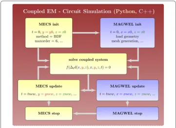
Figure 2 Coupled simulation.Set up for simulating coupled problems involving electromagnetics and circuit equations. Here there is integration between a circuit simulator (MECS) and an EM-solver. Note that the MAGWEL software provides contributions to specific equations as well as associated Jacobian values.
Figure 3 Bond wire.Classic IC lead-frame package.
Figure 4 Bond wire.Bond-wire heat transfer problem.
Above,Twis the wire temperature,Tois the reference (ambient) temperature,ακ is the
temperature coefficient of the wire thermal conductivity, andθwis an auxiliary variable.
esti-ter Maten et al.Journal of Mathematics in Industry (2017) 7:2 Page 6 of 19
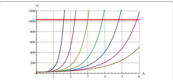
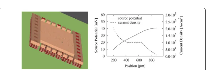
Figure 5 Bond wire.Au-wire current capacities for several diameters and a fixed length. The plotted temperature is at the wire mid-point, where the hottest point is expected.
mated current capacity (temperature vs current amplitude) for a gold wire after ms. The formula retains important geometrical parameters defining the package, which adds high flexibility. This reduces the over-design of the wires during fabrication. The evaluation of this formula is computationally inexpensive such that time-consuming D simulation can be avoided. However, a coupling of the bondwire model to a D simulator is necessary if the integration in the overall system behaviour should be simulated. Thus, TUD also implemented a nonlinear in-house simulation code based on the Finite Integration Tech-nique (FIT) to analyze the coupling before transferring the concept to partner MAG [].
ONNaims to use the algorithm within a GUI (Graphical User Interface).
ONNand BUT made measurements of DC and dynamical fusing of bondwires [].
ONNfabricated test chips (SOIC package so far), where the individual bondwires with different lengths, diameters and materials have been encapsulated. BUT prepared a com-plete methodology and experimental setup to do such investigations.
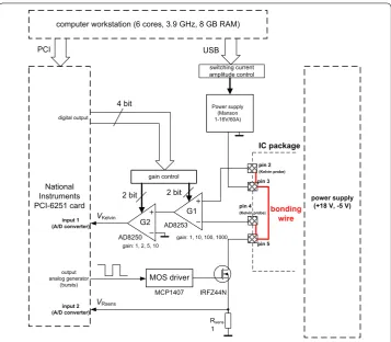
The setup (hardware tester and MATLAB GUI) allows measurements of all six bond-wires in one IC package. The tester consists of the independent channels, the driving stages, the Kelvin probe sensing stages, the demultiplexing core for the driving stages (specification of address of the bondwire) and the multiplexing core for the Kelvin probe sensing stages.
The block structure, the single channel operation and photographs of the final hardware solution are shown in Figure , Figure and Figure . The frequency limitation of the measurement setup is about kHz (limits of the used MOS power-switches and PCI card). The software part of the project consists of two executable MATLAB scripts with a GUI. MATLAB software is also used for the generation of testing sequences and signals that drive the tester. Finally, the measurements have been used to validate the bondwire formula.
2.3 Electro-thermal coupled simulation
large-ter Maten et al.Journal of Mathematics in Industry (2017) 7:2 Page 7 of 19
Figure 6 Bond wire.Final hardware solution of the bondwire tester prototype: overall block structure.
scale (millimeter) structures and the small-scale (sub-micron) of the finger architecture in a single simulation. The computation deals with the coupling of the electrical response and with the thermal response in first-principle field solving. Figure illustrates today’s capabilities [].
2.4 Multirate simulations
In coupled problems one often encounters multiscale differences (in space) and large vari-ations in dynamics in time-domain: multirate effects []. In this book especially partitions in space with different dynamics lead to couplings between subsets of DAEs. A careful formulation of the coupling is key in being able to guarantee convergent dynamical itera-tions in a co-simulation. In [] the partition between physical quantities (electromagnet-ics, heat) was exploited to study this convergence.
ter Maten et al.Journal of Mathematics in Industry (2017) 7:2 Page 8 of 19
Figure 7 Bond wire.Final hardware solution of the bondwire tester prototype: single channel principle.
is a severe bottleneck for PLL simulation and for the multirate technique in general. In de-riving Figure , adaptive methods were employed for the different stages of the divider. Table shows the drastic improvement of the run time using adaptivity. No commercial circuit simulator provides this facility yet.
2.5 Parametric model order reduction
MPGand MAG developed efficient parametric/parameterized Model Order Reduction (pMOR) methods and techniques for fast simulation of electro-thermal coupled models [, ] and for fast Uncertainty Quantification [] of nanoelectronic, electro-thermal models with random variables or stochastic processes. Given the system matrices at dif-ferent values of the parameters or realizations of random variables, we extract system ma-trices which are independent of the parameters (random variables), so that parametric models can be constructed, and the parameters (random variables) symbolically appear in the model. Reduced-order models of the large-scale parametric models are obtained us-ing parametric model order reduction techniques. For general complex geometries, like in Figure , an accurate, physical model in the form of heat transfer partial differential equations is required. The electrical transport is controlled by Ohm’s law and the current continuity equation in conductive material
ter Maten et al.Journal of Mathematics in Industry (2017) 7:2 Page 9 of 19
Figure 8 Bond wire.Final hardware solution of the bondwire tester prototype: final version of the PCB.
Figure 9 Power MOS transistor.Analysis of a power MOS (left figure) resulting into an asymmetric current density due to thermally induced conductance variations in the metallic interconnect (right figure).
The generated-energy transport is controlled by Joule’s law
∂U
∂t = –∇ ·Q+, Q= –κ(T)∇T, U=CV
T–T∗. () Of particular interest is the local heat generation, which is given by
ter Maten et al.Journal of Mathematics in Industry (2017) 7:2 Page 10 of 19
Figure 10 Divider block diagram.A divider block diagram for a PLL (phase lock loop) in the 5.6GHz ISM band (industrial, scientific and medical (ISM) radio band).
Figure 11 Multirate solution.The solutions show time-varying multirate behaviour, which was efficiently solved by the implementation of FHO.
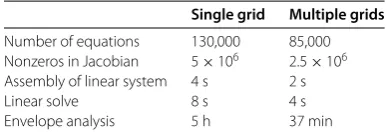
Table 2 Performance summary multirate simulation
Single grid Multiple grids
Number of equations 130,000 85,000 Nonzeros in Jacobian 5×10⁶ 2.5×10⁶ Assembly of linear system 4 s 2 s
Linear solve 8 s 4 s
Envelope analysis 5 h 37 min
Figure 12 A thermal package model(provided by MAG).
Hereκ(T) is the heat diffusion,CVis the constant-volume heat capacitance of the material,
large-ter Maten et al.Journal of Mathematics in Industry (2017) 7:2 Page 11 of 19
scale system of ODEs in the form of
Edx(t)
dt =Ax(t) +x(t)
TFx(t) +Bu(t), ()
where xis the state vector including the nodal voltages and nodal temperatures vary-ing with time. The tensor F∈Rn×n×nrepresents the non-linear character of the heat
source. Roughly speaking,Fcan be considered as a D array ofnmatrices. Each matrix is inRn×n. The matrixE∈Rn×nis a capacity matrix for both the electrical and the
ther-mal part, and the matrixA∈Rn×nis the conductivity matrix for both the electrical and
the thermal part. Linear parametric models in state-space-form were constructed based on the discrete data provided by MAG, resulting from a finite-integration technique (FIT). As an example we consider a parametric thermal package model, see Figure . When con-sidering meshes that are topologically equivalent for different package thicknessesp, the parametric dependence of the matrices as well as the matrices in the tensorF will take the form as
M(p) =M+pM+
pM. ()
The second term in () originates from the linear dependence of dual areas corresponding to the cell edges perpendicular to the thickness, whereas the third term originates from dual areas associated to cell edges tangential to the thickness orientation.
If the parameterpsymbolically appears in the model, the system in () becomes a para-metric model,
E(p)dx(t,p)
dt =A(p)x(t,p) +x(t,p)
TF(p)x(t,p) +B(p)u(t), ()
where the matrixE(p),A(p),B(p) and each matrix inF(p) are in the form ofM(p). Some mathematical calculations are needed to extract the parametric system from the system in (). However, the calculations are independent of the dimension of the matrices in (), which makes the calculation very cheap and flexible [].
Using a robust parametric model order reduction algorithm in [], a reduced paramet-ric model () with the same parametparamet-ric structure as the full parametparamet-ric model, in (), but with much fewer equations, has been derived
ˆ
E(p)dz(t,p)
dt =Aˆ(p)z(t,p) +z(t,p)
TFˆ(p)z(t,p) +Bˆ(p)u(t). ()
ter Maten et al.Journal of Mathematics in Industry (2017) 7:2 Page 12 of 19
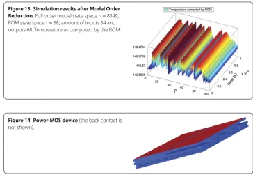
Figure 13 Simulation results after Model Order Reduction.Full order model state spacen= 8549, ROM state spacer= 58, amount of inputs 34 and outputs 68. Temperature as computed by the ROM.
Figure 14 Power-MOS device(the back contact is not shown).
an efficient method: BDSM-ET [], which uses the superposition principle to construct a ROM with block-wise sparsity. The size of the ROM isr= , and thus almost two orders of magnitude smaller than the Full Order Model (FOM). A most important feature is that the ROM is also much sparser than the ROM obtained using the standard method. With an error less than –, the thermal part of the ROM has been used together with
Spectre, and validated to be efficient.
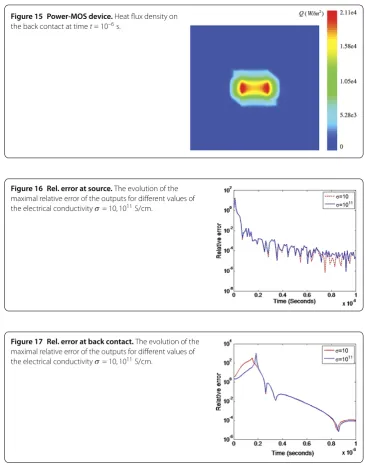
In developing pMOR methods for fast UQ of nanoelectronic, electro-thermal models with random variables or stochastic processes, we applied pMOR techniques to a Power-MOS device (Figure ), provided by MAG, and obtained a parametric reduced order model (pROM) that is of high accuracy over a very large parameter range. We have em-bedded the parametric reduced model into the Stochastic Collocation Method [], which proved to be both efficient and accurate.
Figure displays the Power-MOS chip. Figure shows the heating of the chip. We built an order- pROM for the order- FOM of the electrical part, and an order- pROM for the order- FOM of the thermal part. Figure and Figure depict the evolution of the ‘maximal relative error at the outputs’, which is defined as the maximal relative error at all outputs. When the system starts, the maximal relative error is high because the sys-tem is hardly heated up (exact values close to zero) and the thermal parts are dominated by modelling error and numerical error. However, as time elapses, the maximal relative error goes down to the order of –and therefore, the dominant physical properties are accurately captured over a large parameter range.
2.6 Uncertainty quantification
ter Maten et al.Journal of Mathematics in Industry (2017) 7:2 Page 13 of 19
Figure 15 Power-MOS device.Heat flux density on the back contact at timet= 10–6s.
Figure 16 Rel. error at source.The evolution of the maximal relative error of the outputs for different values of the electrical conductivityσ= 10, 1011S/cm.
Figure 17 Rel. error at back contact.The evolution of the maximal relative error of the outputs for different values of the electrical conductivityσ= 10, 1011S/cm.
ter Maten et al.Journal of Mathematics in Industry (2017) 7:2 Page 14 of 19
Figure 18 Power transistor.Power Transistor optimized to reduce power hotspots while taking geometrical variations into account.
stochastic Partial Differential Equations (PDEs). Its solution enables to investigate the propagation of uncertainties through a -D model, which affect yield and performance of a power transistor. In particular as parametersp(ω) = [σ(ω),W(ω),Cυ(ω),VD(ω),VS(ω)]
are taken, in which the conductivity of the Metal layer,σ, the thickness of the Metal,
W, and the thermal capacitance of the Via,Cυ, and the drain and source contacts are
considered, see also Figure . Hereωvaries over some event space and the probability distributions of the parameters are predetermined. The PDEs are equipped with random Dirichlet boundary conditions that describe the potentials at the drain and source pads.
To reduce the current density overshoots in the area of the contact layer of the power device, as basic random-dependent cost functional
F(υ) =w
D
Qe
υ,V(υ)dx+w
hV(υ)dγ, ()
was taken, where the dissipation powerQeis analyzed in the area of Metal layer D⊂R,
and the source voltage termhis represented by the random Dirichlet boundary condition in the area of the source and drain pads⊂R. The variableυis defined asυ= (x,p(ω)), whereas the weightswandwrefer to known a priori information about objectives.
For the robust optimization one considers a PDE-constrained minimization problem
min
υ E
F(υ)+η
VarF(υ), ()
whereη= was taken. The Stochastic Collocation Method, based on Polynomial Chaos Expansion (PCE) [, ], provided a response surface model to estimate the expectation
E[F(υ)] and the standard deviation√Var[F(υ)]. Combining with a Topological Derivative Method, we could reduce hot spot phenomena in a robust sense, see Figure . The op-timization results for a relevant nanoelectronics problem demonstrate that the proposed method is robust and efficient [].
We finally remark that our implementations are also able to identify dominant parameter contributions to the variance when varying parameters [].
ter Maten et al.Journal of Mathematics in Industry (2017) 7:2 Page 15 of 19
Figure 19 Power transistor.The pictures give a temperature distribution in the Metal3 layer and the Contact Layer for the structure after optimization (joint work by UGW, BUW, MAG).
industry because it is much faster than Monte Carlo. Our UQ implementation exploits sparse grid techniques and can easily deal with up to independent parameters.
2.7 Fast fault simulation
NXP, BUW and TU Eindhoven developed a special algorithm for fast fault simulation in NXP’s in-house circuit simulator Pstar. NXP’s simulator is the best in the world for this functionality [, ]. Imperfections in manufacturing processes may cause unwanted connections (faults) that are added to the nominal, ‘golden’, design of an electronic cir-cuit. When considering faults from the point of view of parameter variations this is well in the range of large deviations. In [] the faulty elements are represented by adding linear conductivities to the circuit. The approach also works for analyzing the effect of additional linear capacitors. However, the main interest is in adding linear conductivities: thuspuvTx(t,p), wherep= /R, with resistanceR, and given vectorsu,v, to the system of
circuit equations of which the solution becomesx(t,p). By fault simulation we simulate all situations: a huge number of new connections of pairs of vectors (u,v) and each with many different values ofp, up to the regime of large deviations, for the newly added el-ement and comparing the resultx(t,p) at specific time points with the ‘golden’ solution
˜
x(t) =x(t, ) of the fault-free circuit, corresponding withp= . If the deviation between
ter Maten et al.Journal of Mathematics in Industry (2017) 7:2 Page 16 of 19
Figure 20 Fast fault imulation.Speed up in fast fault simulation for the TJA1021 chip.
The results are stored in a database. This database is of help to first externally diag-nose a faulty IC and to identify the candidate circuit submodels where the fault may have happened. After that the IC can be studied further internally. This can help to improve next productions. Moreover, the collection of simulations can also be helpful as a priori check before layouting. NXP can identify locations on a chip that are probably affected by tiny manufacturing accuracies, which case faulty behaviour at predefined time points for measurements.
Inclusion of sensitivity analysis brought speeds up in CPU time of a factor or more. See Figure for an indicative result. Later invoking of faults gave an additional order of magnitude in speed up. By this reduction of simulation time candidate faults could be detected that would have been impossible otherwise because of excessive CPU time [].
Note that essentially one is looking to the weak spots in the circuit. In our approach the manufacturing process is the immediate cause of the problem. However it can also show up later, due to effects of ageing of the design, or by stress effects due to heating. It is also related to other network problems, e.g., in analyzing traffic behaviour in a city when suddenly a road is blocked, or when a new connection pops up. Our approach can be extended to energy distribution networks, sewage systems, and even to networks that are not constant of size in time.
This algorithm also offers interesting ingredients to combine with Uncertainty Quan-tification.
2.8 Test examples, measurements
ter Maten et al.Journal of Mathematics in Industry (2017) 7:2 Page 17 of 19
boards. They served for step by step study, for comparison to measurements and for val-idation of the enhanced MAGWEL software, in close cooperation with BUT, NXP and
ONN.
As simple example, we mention here test chips that include passive structures (induc-tances, capaci(induc-tances, baluns, resonators). These structures, that are easily measurable, are used to validate further EM extraction and model reduction. Simulated results are com-pared to measurements, EM solver extraction and then with extraction plus netlist reduc-tion in terms of accuracy, memory usage and time simulareduc-tion.
3 Conclusion
The unique combination of the nanoCOPS consortium allows to already report the fol-lowing intermediate, innovative highlights halfway the project, to which all partners have contributed.
• The coupling interface with the MAGWEL software has been improved, tested and is operational.
• Successful large-scale EM-heat simulation was achieved. • Grid-adaptive multirate circuit simulation was established.
• Model Order Reduction was successfully applied to coupled EM-heat problems. • Accurate bond wire modelling for fast usage at industry was demonstrated and was
validated by measurements.
• Uncertainty Quantification was applied to variations of material parameters and geometry and was used in robust topology optimization. Apart from the topics, this at best demonstrates the robustness of the integrated software - to achieve optimization one addresses all parts of the codes.
• Innovative methods for improving yield as well as to identify faults were derived. • Advanced measurements environments have been set up both at academia and at
industry.
• Outcomes have been presented at conferences. Joint papers have been published in various journals.
• Interaction between academia and industrial partners addressed a broad range: test examples, new algorithms, implementations, practical use of new methods, ways to improve measurements.
The focus in the second half of the project is on further validation and demonstra-tion of the methods by applying them to the broad range of IC building blocks. To-gether with the industry partners methodologies are defined how best to use the meth-ods. All three industrial partners started work on reliability and the impact of age-ing. Also steps to yield optimization have been developed. Techniques with adjoint approaches are currently introduced. Also inverse problems are addressed. Presen-tations will be given at SCEE-, Scientific Computing in Electrical Engineering, http://wwwdev.ricam.oeaw.ac.at/events/conferences/scee/.
Competing interests
The authors declare that they have no competing interests.
Authors’ contributions
ter Maten et al.Journal of Mathematics in Industry (2017) 7:2 Page 18 of 19
Author details
1Bergische Universität Wuppertal, Gauß-Straße 20, Wuppertal, 42119, Germany.2Ernst-Moritz-Arndt-Universität Greifswald, Walther-Rathenau-Straße 47, Greifswald, 17487, Germany.3Humboldt Universität zu Berlin, Unter den Linden 6, Berlin, 10099, Germany.4MAGWEL NV, Vital Decosterstraat 44 bus 27, Leuven, 3000, Belgium.5Max Planck Institut für Dynamik komplexer technischer Systeme, Sandtorstr. 1, Magdeburg, 39106, Germany. 6NXP Semiconductors, High Tech Campus 46, Eindhoven, 5656 AE, The Netherlands.7ON Semiconductor Belgium BVBA, Westerring 15, Oudenaarde, 9700, Belgium. 8Fachhochschule Oberösterreich, Softwarepark 11, Hagenberg im Mühlkreis, 4232, Austria. 9Vysoké u˘cení technické v Brn˘e, Brno University of Technology, Purky ˇnova 464/118, Královo Pole, Brno, 61200, Czech Republic.10Technische Universität Darmstadt, Dolivostraße 15 & Schloßgartenstraße 8, Darmstadt, 64293, Germany. 11ACCO Semiconductor, 36-38 Rue de la Princesse, Louveciennes, 78430, France.
Acknowledgements
This FP7 Collaborative Project nanoCOPS is supported by the European Union in the FP7-ICT-2013-11 Programme under Grant Agreement Number 619166 (Project nanoCOPS - nanoelectronic COupled Problems Solutions). For further details see http://www.fp7-nanocops.eu/.
Received: 10 February 2016 Accepted: 20 June 2016
References
1. Janssen HHJM, Benner P, Bittner K, Brachtendorf H-G, Feng L, ter Maten EJW, Schöps S, Tischendorf C. The European project nanoCOPS for nanoelectronic coupled problems solutions. In: Russo G, Capasso V, Nicosia G, Romano V, editors. Progress in industrial mathematics at ECMI 2014. Mathematics in industry. vol. 22. Berlin: Springer; 2016. 2. Janssen R, ter Maten J, Tischendorf C, Brachtendorf H-G, Bittner K, Schoenmaker W, Benner P, Feng L, Pulch R, Deleu F,
Wieers A. The nanoCOPS project on algorithms for nanoelectronic coupled problems solutions. In: Schreffler B, Oñate E, Papadrakakis M, editors. Coupled problems in science and engineering VI - COUPLED PROBLEMS 2015. Barcelona: CIMNE - International Center for Numerical Methods in Engineering; 2015. p. 1029-36. ISBN 978-84-943928-3-2. 3. Banagaaya N, Feng L, Schoenmaker W, Meuris P, Wieers A, Gillon R, Benner P. Model order reduction for
nanoelectronics coupled problems with many inputs. In: Proceedings of design, automation and test in Europe (DATE). 2016. p. 313-8. Paper 0996.
4. Casper T, De Gersem H, Gotthans T, Schoenmaker W, Schöps S, Wieers A. Electrothermal simulation of bonding wire degradation under uncertain geometries. In: Proceedings of design, automation and test in Europe (DATE). 2016. p. 1297-302. Paper 0776.
5. Putek P, Meuris P, Pulch R, ter Maten EJW, Günther M, Schoenmaker W, Deleu F, Wieers A. Shape optimization of a power MOS device under uncertainties. In: Proceedings of design, automation and test in Europe (DATE). 2016. p. 319-24. Paper 0998.
6. Schoenmaker W, Meuris P, Strohm C, Tischendorf C. Holistic coupled field and circuit simulation. In: Proceedings of design, automation and test in Europe (DATE). 2016. p. 307-12. Paper 0995.
7. Tasi´c B, Dohmen JJ, Janssen R, ter Maten EJW, Beelen TGJ, Pulch R. Fast time-domain simulation for reliable fault detection. In: Proceedings of design, automation and test in Europe (DATE). 2016. p. 301-6. Paper 0994. 8. Duque Guerra DJ, Schöps S. A fractional step method for the dynamic electro-thermal modelling of device
structures. IFAC-PapersOnLine. 2015;48(1):932-3.
9. Kaufmann C, Günther M, Klagges D, Knorrenschild M, Richwin M, Schöps S, ter Maten EJW. Efficient frequency-transient co-simulation of coupled heat-electromagnetic problems. J Math Ind. 2014;4:1.
10. Schoenmaker W, Dupuis O, De Smedt B, Meuris P. Fully-coupled electro-thermal power device fields. In: Russo G, Capasso V, Nicosia G, Romano V, editors. Progress in industrial mathematics at ECMI 2014. Mathematics in industry. vol. 22. Berlin: Springer; 2016.
11. Baumanns S, Jansen L, Selva-Soto M, Tischendorf C. Analysis of semi-discretized differential algebraic equation from coupled circuit device simulation. Comput Appl Math. 2015;34(3):933-55.
12. Strohm C, Tischendorf C. Interface model integrating full-wave Maxwell simulation models into modified nodal equations for circuit simulation. IFAC-PapersOnLine. 2015;48(1):940-1.
13. Duque D, Schöps S, De Gersem H, Wieers A. nanoCOPS: analytical approach for estimating the heating of bond-wires. ECMI Newsletter. 2014;56:70-1. http://www.mafy.lut.fi/EcmiNL/issues.php?action=viewar&ID=353.
14. Nöbauer GT, Mose H. Analytical approach to temperature evaluation in bonding wires and calculation of allowable current. IEEE Trans Adv Packaging. 2000;23(3):426-35.
15. Duque D, Schöps S, Wieers A. An extended analytical approach for the estimation of the heating of bond-wires. In: Russo G, Capasso V, Nicosia G, Romano V, editors. Progress in industrial mathematics at ECMI 2014. Mathematics in industry. vol. 22. Berlin: Springer; 2016.
16. Petrzela J, Sotner R, Gotthans T, Drinovsky J, Kratochvil T, Wieers A, Gillon R. Different DC fusing scenarios of encapsulated bonding wires. Accepted for presentation at SCEE-2016, Scientific Computing in Electrical Engineering, St. Wolfgang / Strobl, Austria.
17. Günther M, editor. Coupled multiscale simulation and optimization in nanoelectronics. Mathematics in industry. vol. 21. Berlin: Springer; 2015.
18. Bittner K, Brachtendorf H-G. Fast algorithms for adaptive free knot spline approximation using nonuniform biorthogonal spline wavelets. SIAM J Sci Comput. 2015;37(2):B283-304.
19. Banagaaya N, Feng L, Meuris P, Schoenmaker W, Benner P. Model order reduction of an electro-thermal package model. IFAC-PapersOnLine. 2015;48(1):934-5.
20. Benner P, Feng L. Model order reduction for coupled problems. Appl Comput Math Int J. 2015;14(1):3-22. 21. Yue Y, Feng L, Meuris P, Schoenmaker W, Benner P. Application of Krylov-type parametric model order reduction in
efficient uncertainty quantification of electro-thermal circuit. In: Proceedings PIERS. 2015. p. 379-84. 22. Feng L, Meuris P, Schoenmaker W, Benner P. Parametric and reduced-oder modeling for the thermal analysis of
ter Maten et al.Journal of Mathematics in Industry (2017) 7:2 Page 19 of 19
23. Benner P, Feng L. A robust algorithm for parametric model order reduction based on implicit moment matching. In: Quarteroni A, Rozza G, editors. Reduced order methods for modeling and computational reduction. Springer MS&A series. vol. 9. Cham: Springer; 2014. p. 159-85.
24. Xiu D. Numerical methods for stochastic computations - a spectral method approach. Princeton: Princeton University Press; 2010.
25. Putek P, Meuris P, Pulch R, ter Maten EJW, Schoenmaker W, Günther M. Uncertainty quantification for robust topology optimization of power transistor devices. IEEE Trans Magn. 2016;52(3):1700104.
26. Dakota 6.3 - Algorithms for design exploration and simulation. Albuquerque, NM, USA: Sandia National Laboratories; 2015. https://dakota.sandia.gov/.
27. Le Maître OP, Knio OM. Spectral methods for uncertainty quantification. With applications to computational fluid dynamics. Dordrecht: Springer; 2010.
28. Pulch R, ter Maten EJW, Augustin F. Sensitivity analysis and model order reduction for random linear dynamical systems. Math Comput Simul. 2015;111:80-95.
29. Zhang H, Chen T-H, Ting M-Y, Li X. Efficient design-specific worst-case corner extraction for integrated circuits. In: IEEE design automation conference (DAC). 2009. p. 386-9.