dividers and development of an event-driven
model for system simulations
Christoph Beyerstedt, Jonas Meier, Fabian Speicher, Ralf Wunderlich, and Stefan Heinen
Integrated Analog Circuits and RF Systems, RWTH Aachen University, Templergraben 55, 52056 Aachen, Germany Correspondence:Christoph Beyerstedt ([email protected])
Received: 31 January 2019 – Accepted: 28 April 2019 – Published: 19 September 2019
Abstract. This paper presents a frequency domain analysis of spurious tones in frequency dividers. The results of the analysis are used to develop an event-driven model for sys-tem simulations which work entirely in the frequency do-main. The proposed approach is able to provide a fast and accurate model in a SystemVerilog/C++ environment which takes the frequency conversion effects of the spurious tones into account. A virtual prototype which includes the model was simulated and due to the fast simulation speed it was possible to determine the influence of spurious tones on the bit error rate in a complex receive scenario.
1 Introduction
The trend in modern system-on-chips (SoCs) is going to-wards integration of many different subsystems on a single die. Especially for integrated RF-transceivers it brings a chal-lenge due to the complex modulation schemes needed for high data rates and flexibility of the system. On the one hand, a high sensitivity for the receivers and a pure spectral mask of the transmitters are crucial, on the other hand, due to the in-tegration of multiple transceive paths with control logic and digital signal processing on one chip, many sources of dig-ital supply noise exist which can couple in sensitive analog blocks and harm the performance of a transceiver (Hung and Muhammad, 2010). One component, which is crucial for ev-ery transceive system is the high frequency clock generation block used for up- and downconversion of the baseband sig-nals. Usually a phase locked loop (PLL) is used for this pur-pose (Elsayed et al., 2013). Ideally the PLL output is a per-fect sine signal but in reality the output signal contains other
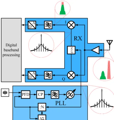
unwanted frequency components due to switching events in-side the blocks and coupling of noise in the components of the PLL (Gao et al., 2010; Lee et al., 2001; Saeed, 2012). In many transceiver architectures the PLL output signal is not directly used but first divided by a frequency divider (FD) before being fed to a mixer. This is advantageous because the pulling of the output power amplifier (PA) on the oscil-lator can be attenuated if the PA output frequency is not the same as the VCO frequency (Razavi, 1999). Furthermore, in complex valued receivers, a frequency divider can be used to generate two local oscillator (LO) signals shifted by 90◦for an IQ mixer (Bardin and Weinreb, 2008).
Figure 1.RF receiver with PLL for LO signal generation.
frequency divider model should not work in the time domain but uses a spectral representation of the signal (see Sect. 3).
2 Analysis
Due to the fact that frequency dividers are strongly nonlinear and have a memory, the conversion of the spurious tones are not straightforward as one would expect. Naively one would say that the frequency of every spectral component just gets divided by the divider factor but frankly this is not the case. A circuit simulation of a frequency divider by two and a divider by three showed, that only the frequency of the main (largest) tone is divided by the divider factor. The spurious component at the offset frequency (foff) of 32 MHz can be found in the output signal at the same offset but with reduced amplitude (see Fig. 2).
A deeper look in the mathematics of spurs and frequency dividers can explain this behavior. The input signal with spu-rious tones of a FD is a quasiperiodic signal with constant amplitude. Simplified, these class of signals can be described as follows:
sin(t )= <{Ainexp(j (ωLOt+φin+φspur(t )))} with:
φspur(t )= N X
i=1
asp,icos(ωsp,it+φsp,i) (1)
Under the assumption that the amplitudesasp,iare small, the
amplitude of the spurious tones can be derived from Eq. (1)
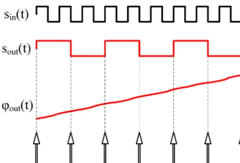
Figure 3.Sampling of the output phase.
by splitting the equation with the trigonometric theorems: As can be seen the spurs originate in the periodic changes in the phase of the clock signal.
sin(t )= <{Ainexp(j (ωLOt+φin+φspur(t )))} = <{Ainexp(j (ωLOt+φin))·exp(j φspur(t ))} ≈ <{Ainexp(j (ωLOt+φin))·(1+j φspur(t ))} =Aincos(ωLOt+φin)+
N X
i=1
<{xi(t )}
with: xi(t )=
j Ainasp,i
2 exp(j ((ωLO−ωsp,i)t+φin−φsp,i)) +j Ainasp,i
2 exp(j ((ωLO+ωsp,i)t+φin+φsp,i)) (2) The output signal of a frequency divider can be easily de-rived from the FD input signal as described in Eq. (1). The FD counts the input rising or falling edges and toggles its output depending on the divider factor N. When looking on the phase of the input and output signal, this behavior can be described by dividing the input phase byN(Egan, 1990). Thus, the output signal of the FD can be described as follows:
sout(t )= <{Aoutexp
jωLOt+φin+φspur(t ) N
} (3)
By splitting Eq. (3) the same way as Eq. (1), the output spec-trum of the FD can be calculated.
sout(t )=Aoutcos
ω
LOt+φin N
+ N X
i=1
<{yi(t )}
with: yi(t )=
j Ainasp,i
2N exp
j
ωLO
N −ωsp,i
t+φin
N −φsp,i
+j Ainasp,i
2 exp
j
ωLO
N +ωsp,i
t+φin
N +φsp,i
(4)
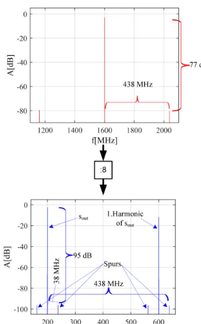
of the spurious tones can only be observed at the transitions of the output signal. Thus, as a good approximation, it can be said that the spurious output tones get sampled by the posi-tive and negaposi-tive edges of the output main signal component of the FD (Apostolidou et al., 2008). Figure 3 gives shows graphically the sampling of the phase by the output main tone. A FD with a divider ratio of 8 and a output duty cycle of 0.5 was simulated on transistor level. The input signal is com-posed of a large tone at 1.6 GHz and a spur at 2.038 GHz. At the output there are not only the downconverted spurious out-put tones but also replica of them in the distance of 400 MHz due to the sampling of the spurs by the edges of the 200 MHz output main tone (Apostolidou et al., 2008). As one can see in Fig. 4 spurious tones with offset frequencies larger than twice the output frequency (438 MHz) can be folded very close to the output main tone and lead to unexpected spurs (38 MHz).
3 Spectral signal description
For understanding the modeling approach of the FD, a small detour to the signal description in the used simulation envi-ronment is necessary. The spectral signal description is sim-ilar to the baseband equivalent signal description, which is a widely used approach to speed up simulations of event-driven real number models of RF systems. It is based on the fact that every modulated RF signal can be represented as: sRF(t )=I (t )cos(ωRFt )−Q(t )sin(ωRFt )
= <{ I (t )+j Q(t )·ej ωRFt} (5) wherefRFis the carrier frequency andI andQdescribes the baseband information (Chen, 2009). The complete informa-tion is inI,Qand the carrier frequency and so it is sufficient to pass the baseband equivalent signal
seq.BB(t )=I (t )+j Q(t )
and the center frequencyfRFbetween the models to recover the full signal. Since the high frequent oscillation ej ωRFt
Figure 4.Simulation result of a FD by 8 with far off spurs.
signal in frequency domain. A solution to this problem is to allow an array of baseband equivalent signal for every car-rier frequency in the signal. To capture nonlinear effects it is also beneficial to store harmonics and possible intermodula-tion products of the frequency components. This is possible by using a multidimensional vector space (Speicher et al., 2018). Furthermore switching between spectral and time do-main can be easily done by using multidimensional fourier transforms. This is advantageous when modeling nonlinear-ities or mixing processes. Like in a harmonic balance simu-lator (Kundert, 1999), the signal is first transformed in time domain, the nonlinearity is applied and the signal is trans-formed back in the spectral domain (see Fig. 5). The spec-tral signal is implemented in a SystemVerilog/C++ modeling framework (see Fig. 6). The advantage of this approach is, that the hardware description language SystemVerilog (SV) can be natively used in the state-of-the-art Cadence EDA en-vironment. A SV model can simply be added to the designed blocks of the system. The structural information of the com-plete design stays the same when using the models instead of the transistor level implementation and the netlist can be reused. Also the event handling can be easily done in SV and does not have to be implemented in another program-ming language. The direct programprogram-ming interface (DPI) of
Figure 5.Example of the processing of nonlinearities.
Figure 6.SV/C++ modeling framework.
SV gives the possibility to access and use functionality of precompiled code of languages like C++. All necessary cal-culations in the models are executed in C++ and benefit from the powerful algorithms and data containers already avail-able there. For the switching between the time and the spec-tral domain, the powerful FFTW library (Frigo and John-son, 2005) is used, which can efficiently execute multidimen-sional fourier transforms. A more detailed description of the spectral signal can be found in Speicher et al. (2018).
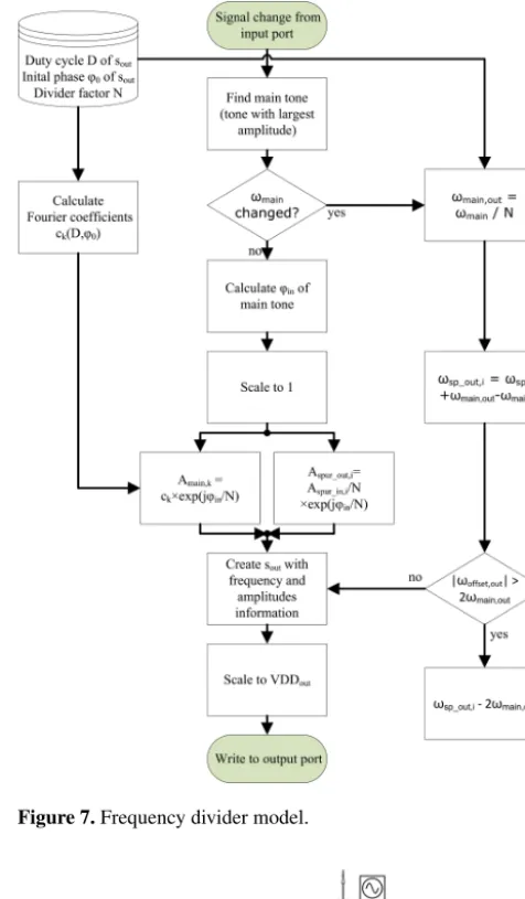
4 Model development
a reasonable size, only the aliasing component of the spurs which are closest to the output main tone and therefore for the most scenarios most critical are attached in the output spectrum. The amplitudes of the output spectrum are calcu-lated separately, depending on whether it is the amplitude of the main tone or it is a spur amplitude. Furthermore, the current, time dependent phase of the input main tone is de-termined. It is coded in the I andQpart of the main tones amplitude. For a fast phase calculation, the current input fre-quency deviation is calculated by differentiation of the input phaseφinof the main tone.
1ωin= d dtφin = d
dtarctan
Q(t )
I (t )
=I (t )Q
0(t )−Q(t )I0(t ) I2(t )+Q2(t ) ≈
I (tn)Q(tntn)−Q(t−tn−n−1)
1 −Q(tn)
I (tn)−I (tn−1)
tn−tn−1
I2(t
n)+Q2(tn)
(7) The output frequency deviation for the main tone can be cal-culated by dividing the input frequency by N. The output phase can be calculated from the output frequency and in-cluded in the calculation of the output amplitudes (see Eq. 4).
1ωout= ωin
N
⇒φout=φout,t0+1ωout(tn−tn−1)
Due to the fact that the input and the output level of the signals might be different, a scaling before and after the am-plitude calculation is done.
5 Example
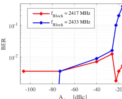
The frequency divider model was used in a virtual prototype of an integrated 2.4 GHz low-if receiver shown in Fig. 8. It consists of an LNA, anI Qmixer driven by a frequency di-vider, which generates theI andQLO signals, a polyphase channel filter and a16-ADC. The output signal of the ADC is fed to a digital demodulator. Furthermore, the digital part contains calibration and control routines and a serial interface to control the chip. Bit error rate simulations of the complete system were done using SystemVerilog/C++ models for the analog components of the receiver. The LO signal was as-sumed to be at 4.8 GHz with spurs at an offset frequency of
Figure 7.Frequency divider model.
Figure 8.Virtual prototype of a 2.4 GHz receiver.
transmit-Figure 9.BER simulation results.
ted bits were simulated per spur level. The simulation speed can be calculated to 10.64 µs simulated time per second. For speed comparison a reference transistor level simulation was run. For 1 µs simulated time it takes 9381s CPU time. Thus the event-driven model is about 99821.7 times faster than the transistor level simulation.
6 Conclusions
In this work a frequency domain analysis of frequency di-viders and an event-driven modeling approach which works with a spectral signal description was presented. The analy-sis focussed on the conversion of spurious tones and showed, that against the intuition the frequency of the spurs are not simply divided by the factor of the frequency divider. It can be shown, that the offset frequency to the main tone stays the same and the spur amplitude gets divided by the divider factor. Furthermore, the sampling of the spurs by the dom-inant output frequency component can lead to unexpected spurs close to the main tone. On basis of these analysis an event-driven frequency divider model was developed which calculates the output in the spectral domain and allows fast system simulations. The model was used in a virtual proto-type of a 2.4 GHz receiver and it was possible to simulate the BER of the system and observe the influence of spurs in the local oscillator signal.
Code availability. Due to the fact that the modeling and verification code is still used in other projects, the code cannot be published.
Data availability. The simulation data of the frequency dividers and the sent and received bitstream for the BER calculation can be found under https://doi.org/10.5281/zenodo.2551231 (Beyerst-edt, 2019).
Competing interests. The authors declare that they have no conflict of interest.
Special issue statement. This article is part of the special issue “Kleinheubacher Berichte 2018”. It is a result of the Klein-heubacher Tagung 2018, Miltenberg, Germany, 24–26 September 2018.
Review statement. This paper was edited by Jens Anders and re-viewed by two anonymous referees.
References
Apostolidou, M., Baltus, P. G. M., and Vaucher, C. S.: Phase noise in frequency divider circuits, in: 2008 IEEE Inter-national Symposium on Circuits and Systems, 2538–2541, https://doi.org/10.1109/ISCAS.2008.4541973, 2008.
Bardin, J. C. and Weinreb, S.: A 0.5–20 GHz quadra-ture downconverter, in: 2008 IEEE Bipolar/BiCMOS Circuits and Technology Meeting, 186–189, https://doi.org/10.1109/BIPOL.2008.4662740, 2008.
Beyerstedt, C.: Frequency Divider and BER simulation data [Data set], Zenodo, https://doi.org/10.5281/zenodo.2551231, 2019. Chen, J. E.: A modeling methodology for verifying
func-tionality of a wireless chip, in: 2009 IEEE Behav-ioral Modeling and Simulation Workshop, 96–101, https://doi.org/10.1109/BMAS.2009.5338880, 2009.
Egan, W. F.: Modeling phase noise in frequency dividers, IEEE T. Ultrason. Ferr., 37, 307–315, https://doi.org/10.1109/58.56498, 1990.
Elsayed, M. M., Abdul-Latif, M., and Sánchez-Sinencio, E.: A Spur Frequency Boosting PLL With a−74 dBc Reference Spur Sup-pression in 90 nm Digital CMOS, IEEE J. Solid-St. Circ., 48, 2104–2117, https://doi.org/10.1109/JSSC.2013.2266865, 2013. Frigo, M. and Johnson, S.: The Design and
im-plementation of FFTW3, P. IEEE, 93, 216–231, https://doi.org/10.1109/JPROC.2004.840301, 2005.
Gao, X., Klumperink, E. A. M., Socci, G., Bohsali, M., and Nauta, B.: Spur Reduction Techniques for Phase-Locked Loops Exploit-ing A Sub-SamplExploit-ing Phase Detector, IEEE J. Solid-St. Circ., 45, 1809–1821, https://doi.org/10.1109/JSSC.2010.2053094, 2010. Hung, C. and Muhammad, K.: RF/analog and digital faceoff –
friends or enemies in an RF SoC, in: Proceedings of 2010 Inter-national Symposium on VLSI Technology, System and Applica-tion, 19–20, https://doi.org/10.1109/VTSA.2010.5488968, 2010. Kundert, K. S.: Introduction to RF simulation and its application, IEEE J. Solid-St. Circ., 34, 1298–1319, https://doi.org/10.1109/4.782091, 1999.
Lee, C.-H., McClellan, K., and Choma, J.: A supply-noise-insensitive CMOS PLL with a voltage regulator using DC-DC capacitive converter, IEEE J. Solid-St. Circ, 36, 1453–1463, https://doi.org/10.1109/4.953473, 2001.