REALIZATION OF DYNAMIC DOUBLE-TILE COMPARATOR PROPOSED FOR
HIGH SPEED 4G NETWORK COMS APPLICATION
Merugu Chandramouli*, VaddeArunaRai
*Department of Computer Engineering, Eritrea Institute of Technology, Mai nefhi, Asmara, Eritrea.
Department of Electrical and Electronics Engineering, Eritrea Institute of Technology, Mai nefhi, Asmara, Eritrea.
KEYWORDS
:
dynamic clocked comparator, Double-tail comparator, low-power analog design high-speed analog-to-digital converters (ADCs).ABSTRACT
In the current circumstance, necessity for ultra-low-control, domain capable and quick easy to-cutting edge converters (ADCs) is pushing toward the use of component Clocked regenerative comparators to improve the power profitability and pace. In this work, we changed the structure of the Dynamic Double-Tile Comparator by adding couple of additional transistors to the present structure. The proposed changed Double-Tail Dynamic Comparator is used for fast operations even as a piece of little supplies voltages. We can execute the proposed structure and existing structures of Dynamic Comparator in Mentor Graphics Tool. From entertainment results in 0.18-μm CMOS advancement, we find that the proposed arrangement yields less Delay than the present structures.
INTRODUCTION
Comparator is one of the crucial building obstructs in the vast majority of the simple to-computerized converters (ADCs) [1]. Numerous high speeds ADCs, for example, streak ADCs require low power fast comparators with in a little chip zone. Fast comparators in ultra-profound sub micrometer (UDSM) CMOS innovations experience the ill effects of low supply voltages particularly while considering actuality that edge voltages of the gadgets have not been scaled at the equivalent pace as the supply voltages of the advanced CMOS forms[2,3]. Thus, planning rapid comparators is various difficulties, when the supply voltage is littler. At the end of the day, in an offered innovation to accomplish rapid, bigger transistors are expected to repay the diminishment of supply voltage, which likewise implies that more power and bite the dust range is required[4]. Moreover, low-voltage process results in restricted basic mode data range, which is extremely noteworthy in some rapid simple to-computerized converter models, for example, streak two-stage, collapsing ADCs. Different procedures, for example, supply boosting strategies, systems utilize body-driven transistors, current-mode plan and those utilizing double oxide forms, which can deal with extremely higher supply voltages have been produced to get together the low-voltage outline challenges [5]. Boosting and bootstrapping are the two methods in view of increasing the clock voltage or supply, reference to address exchanging issues and info range [6]. These are compelling systems, yet they present unwavering quality issues particularly in UDSM CMOS advancements. Body-driven procedure embraced that evacuate the limit voltage prerequisites such that body driven MOSFET works as exhaustion sort gadget [6, 7]. the body driven transistor's experiences the littler trans conductance (equivalent to the gmb of the transistor) contrasted with its entryway driven partner while uncommon manufacture procedure, for example, a profound n-well is needed both pMOS and nMOS transistors are work in body-driven design. Separated from technological changes, creating novel circuit structures which abstain from stacking an excess of transistors between supply rails is best for a low-voltage operation, particularly in the event that they don't build the circuit unpredictability [8]. In extra hardware is added to the customary element comparator to upgrade the comparator speed in low supply voltages. The structure of twofold tail dynamic comparator initially proposed depends on the planning separate information and cross coupled stage. This partition is empowers the quick operation over a wide supply voltage range [9, 10].
CLOCKED REGENERATIVE COMPARATORS
The Clocked regenerative comparators have discovered wide applications, some fast simple to-advanced converter structures since they can settle on rapid choices because of the solid positive input in the regenerative lock. As of late numerous exhaustive examinations have been introduced, which explore the execution of these comparators from the diverse viewpoints, for example, power dispersal and time delay investigation is displayed here, the postponement time of two basic structures i.e., customary single-tail element comparator and traditional element twofold tail comparator's are dissected in light of which the proposed comparator will be reachable (exhibited).
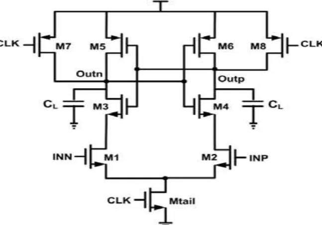
Traditional single-tail Dynamic Comparator: The schematic graph of customary single-tail element comparator extensively utilized as a part of simple to - computerized converters, with rail-to-rail yield swing, high information impedance, and no static force utilization is appeared in the Fig. 1. The operation of the ordinary single-tail element comparator is as per the following. Amid the reset stage when the CLK = 0 and Mtail is off, reset transistors (M7–M8) pull both yield hubs OuputN and OutputP to VDD(0.8v) to characterize a begin condition, this is legitimate coherent level amid reset stage. In the Comparison stage, when VDD = CLK, transistors M7 and M8 are off condition, and Mtail is on state. Yield voltages (OuputN and OutputP), which had been pre-charged to VDD, begin to the release with various releasing rates relying upon comparing info voltage (inputN/inputP). Expecting the situation where VinputP > VinputN, OutputP releases sooner than OuputN thus when OutputP (released by the transistor M2 channel current), tumbles down to the VDD–|Vthp|.Before OuputN (released by the transistor M1 channel current), the relating pMOS transistor (M5) will turn on start the lock recovery brought on by consecutive inverters (M3, M5 and M4, M6). In this way OuputN pulls to VDD and OutputP releases to ground. On the off chance that Vinputp < Vinputn the circuits fills in as the other way around.
Fig. 1. Schematic diagram of the conventional single-tail dynamic comparator
Fig. 2. Transient simulations of the conventional single-tail dynamic comparator Vcm = 0.7 V, and VDD = 0.8 V.
The second term, tlatch, is the latching delay of two cross coupled inverters. It is assumed that a voltage swing of Vout = VDD/2 has to be obtained from an initial output voltage difference V0 at the falling output (e.g., Outp). Half of the supply voltage is considered to be the threshold voltage of the comparator following inverter or SR latch.
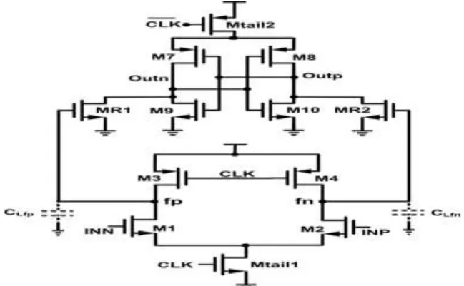
Traditional Double-Tail Dynamic Comparator: The schematic outline of Conventional twofold tail comparator is appeared in Fig. 3. This topology has less stacking and in this way can work little supply voltages contrast with the routine single-tail element comparator. The twofold tail empowers both substantial streams in the locking stage and more extensive Mtail2, for a quick hooking is free of data normal mode voltage , and a lower current in the information stage (little Mtail1), for low counterbalance voltages. The operation of Conventional twofold tail comparator is as per the following. Amid reset period (CLK = 0, and Mtail2 and Mtail1off), transistors M4-M3 pre-charge fp and fn hubs to VDD, which thusly causes transistors MR2 and MR1 to release the yield hubs to ground. Amid choice making stage (CLK = VDD = 0.8v, Mtail1 and Mtail2 turn on), M4-M3 turn off and voltages at hubs fp and fn begin to drop with the rate is characterized by IMtail1/Cfn(p) and on top of this, an info subordinate differential voltage Vfn(p) will develop. The middle of the road stages shaped by MR2 and MR1 passes Vfn(p) to the cross coupled inverters furthermore gives great protecting in the middle of yield's and input's, bringing about lessened estimation of kickback clamor
.
The reenactment aftereffect of customary twofold tail dynamic comparator as appeared in Fig. 4, Similar to the ordinary single-tail element comparator, the postponement of this Conventional twofold tail comparator involves two principle parts, tlatch and t0.The delay t0 allude to the capacitive charging of the heap capacitance (Clout) (at the hook stage yield hubs OutputN and OutputP) until the main n-channel transistor (M10/M9) turns on, after which the lock recovery begins. The recovery time (tlatch) begins after first n-channel transistor of the lock turns on condition(for example M9), the relating yield will be released to the ground, driving front p-channel transistor (e.g., M8) to turn on condition, charging another yield (OutputP) to the supply voltage VDD.
Fig. 4. Transient simulations of the conventional double-tail dynamic comparator for input voltage difference of Vcm = 0.7 V, and VDD = 0.8 V.
In this comparator both intermediate stage transistors will be finally cut-off state, (since fp and fn nodes both are discharge to the ground), hence they do not play any significant role in improving effective transconductance of the latch. Besides, during the reset phase these nodes have to be charged from ground to VDD, which means power consumption.
PROPOSED DOUBLE-TAIL DYNAMIC COMPARATOR
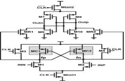
The Fig. 5 demonstrates the schematic diagram of the proposed dynamic double-tail comparator. Due to the better performance of double-tail comparator architecture in low-voltage applications, the proposed comparator is designed based on the double-tail configuration. The main idea of the proposed comparator is to increase Vfn/fp in order to increase latch regeneration speed. For this purpose, we have to add two control transistors (Mc2 and Mc1) of first stage in parallel to M3/M4 transistors but in a cross-coupled manner [see Fig.5].
Operation of the Proposed Comparator: The operation of proposed comparator is as per the following: During reset period (CLK = 0, Mtail1 and Mtail2 are off condition, evading static force utilization), M4 and M3 pulls both fp and fn hubs to VDD, henceforth transistors Mc1 and Mc2 are cut off state. Middle of the road stage transistors, MR1 and MR2 are reset both lock yields to ground. Amid choice making stage (CLK = VDD=0.8v, Mtail2, and Mtail1 are on state), transistors M3 and M4 turn off. Besides toward the start of this stage, the control transistors are still off condition (subsequent to fp and fn are about VDD). In this manner fp and fn begin to drop with the distinctive rates as per the info voltages (inputp and inputn).Suppose Vinputp > V inputn, in this manner the fn drops quicker than fp, (since M2 gives more present than M1current). For whatever length of time that fn keeps falling, the comparing pMOS control transistor Mc1 begins to turn on, pulling fp hub back to the VDD, so another control transistor Mc2 stays off state, permitting fn to be a released totally. At the end of the day, not at all like customary twofold tail dynamic comparator, in which Vfn/fp is only a component of an info transistor transconductance and data voltage distinction, the proposed structure when the comparator recognize that for example hub fn releases speedier, a pMOS transistor Mc1 turns on, pulling other hub fp back to the VDD. Along these lines when passing the contrast in the middle of fp and fn (Vfn/fp) increments in an exponential way, prompting the reduction of the hook recovery time.
Fig.6. Layout of the proposed double-tail dynamic comparator
PERFORMANCE ANALYSYS
In order to compare the proposed dynamic comparator with the single-tail and conventional double-tail dynamic comparator, all circuits have been simulated in a 0.18-μm CMOS technology with VDD = 0.8 V. Table I and Fig.8 compares the performance of the proposed comparator with single-tail and the conventional double-tail dynamic comparators. In 0.18-μm CMOS technology, the proposed comparator provides the less delay at 0.8V supply voltage.
Comparator structure Conventional single-tail Dynamic Comparator
Conventional Double-tail Dynamic Comparator
Proposed Dynamic Comparator
CMOS Technology 180 nm 180 nm 180 nm
Supply Voltage 0.8 V 0.8 V 0.8 V
Maximum Sampling
Frequency 1 GHz 2 GHz 2.4 GHz
Power Dissipation 5.8606 pw 11.0453 pw 11.0453 pw
Delay 422.23ps 291.64ps 266.66ps
Number of Transistors 9 12 14
Fig.8.Comparison of Dynamic comparator Architectures
CONCLUSION
REFERENCES
1. Samaneh Babayan-Mashhadi and Reza Lotfi,” Analysis and Design of a Low-Voltage Low-Powe Double-Tail Comparator” IEEE Transactions on Very Large Scale Integration (VLSI) Systems, vol. 22, no. 2, February 2014
2. S. U. Ay, “A sub-1 volt 10-bit supply boosted SAR ADC design in standard CMOS,” Int. J. Analog Integr. Circuits Signal Process., vol. 66, no. 2, pp. 213–221, Feb. 2011.
3. Mesgarani, M. N. Alam, F. Z. Nelson, and S. U. Ay, “Supply boosting technique for designing very low-voltage mixed-signal circuits in standard CMOS,” in Proc. IEEE Int. Midwest Symp. CircuitsSyst. Dig. Tech. Papers, Aug. 2010, pp. 893–896.
4. J. Blalock, “Body-driving as a Low-Voltage Analog Design Techniquefor CMOS technology,” in Proc. IEEE Southwest Symp. MixedSignal
5. M. Maymandi-Nejad and M. Sachdev, “1-bit quantiser with rail to rail input range for sub-1V modulators,” IEEE Electron. Lett., vol. 39, no. 12, pp. 894–895, Jan. 2003.
6. Goll and H. Zimmermann, “A 0.12 μm CMOS comparator requiring 0.5V at 600MHz and 1.5V at 6 GHz,” in Proc. IEEE Int. Solid-State Circuits Conf., Dig. Tech. Papers, Feb. 2007, pp. 316–317. 7. B.Goll and H. Zimmermann, “A 65nm CMOS comparator with modified latch to achieve
7GHz/1.3mW at 1.2V and 700MHz/47μW at 0.6V,” in Proc. IEEE Int. Solid-State Circuits Conf. Dig. Tech. Papers, Feb. 2009, pp. 328–329.
8. B. Goll and H. Zimmermann, “Low-power 600MHz comparator for 0.5 V supply voltage in 0.12 μm CMOS,” IEEE Electr Lett., vol. 43,no. 7, pp. 388–390, Mar. 2007.
9. D. Shinkel, E. Mensink, E. Klumperink, E. van Tuijl, and B. Nauta, “A double-tail latch-type voltage sense amplifier with 18ps Setup+Hold time,” in Proc. IEEE Int. Solid-State Circuits Conf., Dig. Tech. Papers, Feb. 2007, pp. 314–315.
10. P. Nuzzo, F. D. Bernardinis, P. Terreni, and G. Van der Plas, “Noiseanalysis of regenerative comparators for reconfigurable ADC architectures,” IEEE Trans. Circuits Syst. I, Reg. Papers, vol. 55, no. 6, pp. 1441–1454, Jul. 2008.
11. Nikoozadeh and B. Murmann, “An analysis of latched comaprator offset due to load capacitor mismatch,” IEEE Trans. Circuits Syst.II, Exp. Briefs, vol. 53, no. 12, pp. 1398–1402, Dec. 2006. 12. S. Babayan-Mashhadi and R. Lotfi, “An offset cancellation technique for comparators using