http://www.sciencepublishinggroup.com/j/am doi: 10.11648/j.am.20190804.17
ISSN: 2327-2503 (Print); ISSN: 2327-252X (Online)
Gas Ingress and Egress of MEMS Multi-Chip Modules and
MEMS Devices
Lu Fang
*, Lyle Alexander Menk
Department of Microsystems Integration, Sandia National Laboratories, Albuquerque, USA
Email address:
*
Corresponding author
To cite this article:
Lu Fang, Lyle Alexander Menk. Gas Ingress and Egress of MEMS Multi-Chip Modules and MEMS Devices. Advances in Materials.
Vol. 8, No. 4, 2019, pp. 176-182. doi: 10.11648/j.am.20190804.17
Received: November 12, 2019; Accepted: December 5, 2019; Published: December 13, 2019
Abstract:
Hermetic microcircuit packaging was the dominant method of protecting semiconductor devices in the 1960s and 1970s. After losing majority market sectors to plastic encapsulated microelectronics over the last a few decades, hermetic packaging remains the preferred method of protecting semiconductor devices for critical applications such as in military, space, and medical fields, where components and systems are required to serve for several decades. MEMS devices impose additional challenges to packaging by requiring specific internal cavity pressures to function properly or deliver the needed quality (Q) factors. In MEMS multichip modules, internal pressure requirement conflicts arise when different MEMS devices require different internal gases and pressures. The authors developed a closed-formed equation to model pressure changes of hermetic enclosures due to gas ingression. This article expands the authors mathematical model to calculate gas pressure of a MEMS multichip module package as well as those of MEMS devices inside the multichip module package. These equations are not only capable of calculating service lifetimes of MEMS devices and multi-chip modules but can also help develop MEMS device packaging strategies to extend the service life of MEMS multi-chip modules.Keywords:
Gas Leak, Ingress, Egress, Hermetic Package, MEMS, MCM, Reliability1. Introduction
Hermetic packaging of semiconductor components for critical and long-service life applications remains the preferred packaging method, while most semiconductor devices for consumer and commercial uses are packaged in plastics. This is especially true for some MEMS devices that require certain internal gases and/or gas pressure ranges. Examples of MEMS devices that require hermetic packaging include gyroscopes [1], RF switches [2, 3], RF phase shifters [4], oscillators [5], and IR sensors [6]. To achieve a high Q factor, vacuum needs to be sealed in certain MEMS cavities or packages [7-13]. Often, getters are integrated in the package to maintain vacuum levels by adsorbing or absorbing outgassed species within the package or die cavity [14]. There is another class of MEMS device which requires more positive pressures in the cavity to dampen the ringing of the moving structures [15, 16].
To reduce impedance of transmission lines among
different devices and reduce component sizes, multiple devices are co-packaged in close proximity in one package to form a multi-chip module (MCM). Complications could arise when MEMS requiring vacuum and MEMS requiring a higher working gas pressure are co-packaged in the same MCM. Wafer-level capping of the MEMS devices in their own hermetic cavities can mitigate this gas pressure conflict for a short period of time. However, these devices in the MCM package will eventually affect each other through gas ingresses and egresses. In addition to internal gas exchanges, ambient air will also leak into the MCM package and change the common environment of the individual MEMS devices.
packages [17]. The current article expands the equation to gas ingress and egress of individual MEMS packaged inside the MEMS MCM housing.
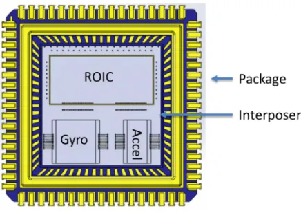
The updated equation herein can be used to calculate gas pressure and vacuum level of each MEMS device in Figure 1 and to determine if all the devices individually and the MCM would meet the required service life requirements. The authors demonstrate the utility of the equation in developing packaging strategies by balancing the pressures of the MEMS devices and the MCM cavity to achieve the performance and lifetime requirements. An equivalent gas pressure concept is proposed and choices of gases in some MEMS devices are explored.
This article embodies the derivations of mathematical equations that govern gas ingress and egress of MCM packages and individual MEMS devices based on first principles. Reports with future experimental results will be published elsewhere.
2. MEMS MCM Descriptions and Gas
Pressure Equations
2.1. MEMS MCM Description
To demonstrate the utility of the equation presented in this article, a MEMS MCM model is first introduced. The hermetically sealed MEMS MCM contains a gyroscope MEMS, an accelerometer MEMS, and a read-out IC (ROIC), Figure 1. These devices are attached on a silicon interposer. Electrical routing among the devices is achieved through wire bonds and traces on the interposer. The ROIC receives and processes signals from the MEMS and reports the results to the system.
Figure 1. MEMS MCM floor plan.
The gyroscope and accelerometer MEMS as seen in Figure 1 are sealed in their own hermetic cavities through wafer-level lidding processes. The initial gas pressure within a typical gyroscope MEMS cavity is nominally 1 mtorr. The pressure within a typical accelerometer MEMS cavity is nominally 760 torr. The initial gas pressure in the MCM package is also at the millitorr level, but for this illustration is slightly greater than that of the gyroscope MEMS cavity. In this situation, air will
thus ingress into the MCM package cavity, while gases in the package cavity will ingress into the gyroscope MEMS, hence the gyroscope MEMS can be regarded as a gas drain. Adhering to the above-described scenario, the gyroscope will be referred to as the drain in this article. Gases in the accelerometer MEMS will leak out into the MCM package cavity. In the same vein, the accelerometer MEMS is a gas source MEMS, source MEMS, or source. Gas pressure changes due to outgassing and getter absorption are outside the scope of this article.
2.2. MEMS MCM Package Cavity Pressure Equation
Equation (1) summarizes the MCM package cavity gas pressure change according to the gas flow directions described above:
∆ ∆ (1) where is the MCM package cavity pressure increase due to external air ingress. ∆ is the package cavity pressure increase due to gas egress from the gas source MEMS. ∆ is the package cavity pressure reduction due to gas leakage from the MCM cavity into the gas drain MEMS. Gas flow rates are all in the fine-leak domain. According to Fang and Menk [17], the first term on the right-hand side of (1) is:
, 1 exp # $, !" !" %&&'()*
+ , -.
, (2)
where is the MCM package cavity gas pressure at time t due to air ingression from the atmosphere, is the atmospheric pressure outside the package, , is the initial gas pressure inside the package, / is the measured helium leak rate of the package after bombing at 0, , V is the package cavity free volume. 12 and 13 are the molecular weights of helium and air, respectively.
The initial gas partial pressure in the gas source MEMS is greater than that inside the package cavity. As shown by Howl and Mann [18], the gas flow rate from a high-pressure enclosure to a low-pressure surrounding is:
#45 4
56 7 %
8 &*
+ ,
(3)
where 9 and are the source cavity free volume and the gas pressure of the gas source MEMS, respectively. C is the gas conductance of the leak channels of the source MEMS seal, T
is absolute temperature, M is the molecular weight of the gas sealed in the MEMS cavity, and is the MCM package cavity gas pressure. Integrating (3) from time 0 to t and rearranging for :
, , 1 exp #:4%&8*
+ , -.
(4)
where , is the initial gas pressure of the gas source MEMS cavity. If the source MEMS cavity is sealed with PO = 1 atm
leak rate from the MEMS cavity into the package is:
; 7 &8) +, < (5)
Substituting (5) into (4):
, − ( , − ) 1 − exp −#4 =%&&)*
+ , -. (6)
And from fundamental gas kinetics theory [19]:
;>13= ;2 >12 (7)
and observing:
;2 = $= (8)
Plugging (7) and (8) into (6), the MEMS cavity pressure at time t is:
= , − ( , − ) 1 − exp −#4 $,44 %&&'(*
+ , -. (9)
From time 0 to time t, MEMS cavity pressure decreases by:
(10)
The amount of gas to leak out of the source MEMS is:
? =∆ 4#4
8 (11)
This is also the amount of gas transferred to the MCM package cavity, therefore:
∆ 9 = ∆ 9 (12) The package pressure increase due to gas source MEMS contribution is:
∆ =∆ 4#4
# !" (13)
Plugging (10) in (13):
∆ = #4
# !"( , − ) 1 − exp − 4
#4 $,4%
&'(
& *
+ , -.
(14)
Equation (14) is the second item of the right-hand side of (1).
As described by Fang and Menk equation, gas pressure of
the gas drain MEMS follows:
( ) = − , 1 − exp −# $,@@ %&&'()* + , -. +
, (15)
where , is the initial gas pressure of the gas drain MEMS cavity. / is the measured drain MEMS helium leak rate after bombing at 0, . The pressure change at time t is:
∆ = ( ) − , =
− , 1 − exp −# $,@@ %&&'()*
+ , -.
(16)
As with (11), the amount of gas leaked into the gas drain MEMS from the MCM package cavity is:
? =∆ @#@
8 (17)
This causes the package cavity pressure to decrease by:
∆ =∆ @#@
# !" (18)
Plugging (16) into (18), the package cavity gas pressure reduction due to gas loss to the gas drain MEMS is:
∆ = #@
# !" − , 1 − exp − @ # $,@%
&'( &)*
+
, -. (19)
Plugging (2), (14), and (19) into (1), the gas pressure of the MCM package cavity with source and drain MEMS at time t is:
= − , 1 − exp −# $, !" !" %&&'()*
+ , -. +
, +## !"4 ( , − ) 1 − exp −#4 $,44 %&&'(*
+ , -. −
#@
# !" − , 1 − exp −
@
# $,@%
&'(
&)* + , -.
(20)
2.3. Application of MEMS MCM Package Cavity Pressure Equation
For demonstration purposes, Table 1 lists example cavity sizes, initial gas pressures, and helium leak rates of the MCM package, gas source MEMS, and gas drain MEMS. Helium bombing pressure used in all leak rate testing is 5.1 atm.
Table 1. Package and MEMS information.
Item Cavity size, cc Initial gas pressure, atm Helium leak rate, atm cc/sec
MCM package 0.7513 1.32E-03 3.5E-12
Gas source MEMS 0.0053 1.0 5.6E-11
Gas drain MEMS 0.007 1.00E-06 5.6E-11
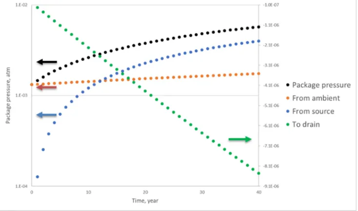
Figure 2 shows annual gas pressure increase of the MCM package and the contributions of atmospheric air ingress, gas source MEMS, and gas drain MEMS as described in (20). As air leaks into the MCM package, the cavity gas pressure
increases. When this occurs, the driving force of further gas ingress decreases and, therefore, the amount of annual MCM cavity gas pressure increase reduces year after year. This phenomenon is also observed on the trend of the annual gas
∆
A=
A,B−
A= (
A,B−
CD) 1 − exp −
9A E,A/A%
11FG*
contribution from the source MEMS. Gas pressure of the source MEMS decreases more quickly because of its greater gas leak rate and the smaller cavity volume as compared to that of the MCM package. These factors compound on the ability of the gas source MEMS to further contribute gas to the MCM cavity. The increase of gas pressure in the MCM package cavity increases the driving force of gas ingress into
the drain MEMS, hence the slope of the corresponding line is slightly positive. Since gas egress from the source MEMS into the MCM package dominates the MCM cavity pressure change during this period, the annual package cavity pressure curve follows the trend of that of the source MEMS contribution curve as seen in Figure 2.
Figure 2. Annual gas pressure increases of MEMS multi-chip module package and the contributions of the source and drain MEMS.
Figure 3 depicts the cumulative gas pressure changes in the MCM package cavity. The increase of package gas pressure, the contribution of air ingress from atmosphere, and the contribution of the gas source MEMS are read from the primary vertical axis, which is logarithmic. Air ingress from atmosphere and gas egress from the source MEMS cause the
MCM package cavity pressure to increase over time. The MCM package gas leaks into the drain MEMS as read from the secondary vertical axis, which is linear, in Figure 3. This leak rate is orders of magnitude smaller compared to the amount of gases ingress into the MCM cavity from atmosphere and the source MEMS.
Figure 3. Cumulative gas pressure changes of MCM package cavity and its contributors.
2.4. Gas Pressures of the Gas Source and Drain MEMS Cavities
With a known cavity pressure in the MEMS MCM package, pressures of the gas source MEMS and gas drain MEMS can be calculated using (9) and (15), respectively. Figure 4 shows
above 0.85 atm, it is clear from Figure 4 that the gas drain MEMS device would continue to perform at the required Q factor level for much longer than 40 years. The gas source
MEMS device, on the other hand, could only function for less than 8 years.
Figure 4. Cavity gas pressure of MEMS multi-chip module package, gas source MEMS, and gas drain MEMS.
2.5. Strategies to Extend Service Life of the Gas Source MEMS
2.5.1. Reduction in Leak Rate of Gas Source MEMS
Figure 5. Service extending effects by reducing gas leak rate and using heavier gas.
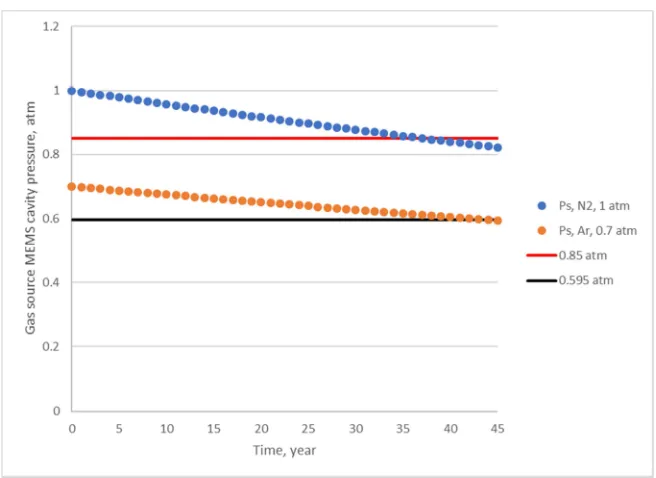
The most effective approach to extend the service life of the gas source MEMS is to seal the MEMS devices better and reduce the gas leak rate, / . The upper curve of Figure 5 shows that, by reducing / from 5.6×10⁻¹¹ atm cc/sec He to 1×10-11 atm cc/sec He, the source MEMS cavity pressure can be maintained above 0.85 atm for 37 years.
2.5.2. Seal Heavier Gases in Source MEMS
Equation (9) reveals an important strategy one could exploit to extend the source MEMS service life. The most commonly used gas in a source MEMS cavity is nitrogen, and the initial filling pressure is typically 1 atm. Nitrogen gas molecules
source MEMS and would thus prolong the time it takes for Argon pressure in the source MEMS cavity pressure to drop to 85% of the initial gas pressure. This strategy maintains the gas damping effect and extends the service life of the source MEMS. The lower curve in Figure 5 shows that by initially filling the source MEMS cavity with 0.7 atm argon, one could extend the service life of the source MEMS from 37 years to 44 years.
2.5.3. Increase Initial Source MEMS Gas Pressure
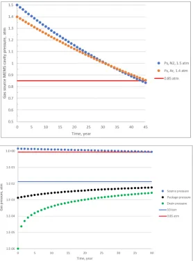
If the lowest leak rate of a source MEMS is 3×10-11 atm cc/sec He, one can also take an opposite approach to that shown above and increase the initial gas pressure of the source MEMS cavity. Using (9), one can easily find the initial nitrogen or argon pressures for the source MEMS to guarantee that, at the expected end of service life, the source MEMS would function at the requested performance level. Figure 6 shows that by setting the initial pressure of 1.5 atm and 1.4 atm for nitrogen and argon, respectively, the source MEMS cavity pressure will be above 0.85 atm for more than 40 years. When employing this approach, one needs to use (20) to verify
that the drain MEMS pressure is not pushed above its working pressure limit. Of course, this approach may require facility and process adjustments. Equation (20) demonstrates an effective method to develop and verify MEMS MCM packaging strategies to meet service life requirements.
3. Conclusion
The authors have developed a closed-form gas pressure equation that governs gas pressure of MCM packages as well as those of gas source and gas drain MEMS devices inside the MCM packages. Examples are given to demonstrate the applications of the equation to MEMS MCM and its pieces to gas source and gas drain MEMS devices. Packaging engineers can use the equation to develop MCM packaging strategies. System and reliability engineers can use this work to verify that the gas source and gas drain components can deliver the required functionality and performances throughout the required MEMS MCM service life.
Figure 6. Effects of increase of the initial source MEMS cavity pressure on the internal pressures of the MEMS devices.
Acknowledgements
Sandia National Laboratories is a multimission laboratory managed and operated by National Technology and Engineering Solutions of Sandia LLC, a wholly owned subsidiary of Honeywell International Inc. for the U.S. Department of Energy’s National Nuclear Security Administration under contract DE-NA0003525. This paper describes objective technical results and analysis. Any subjective views or opinions that might be expressed in the paper do not necessarily represent the views of the U.S. Department of Energy or the United States Government.
References
[1] T. K. Tang, R. C. Gutierrez, C. B. Stell, V. Vorperian, G. A. Arakaki, J. T. Rice, W. J. Li, I. Chakraborty, K. Shcheglov and J. Z. Wilcox, "A PACKAGED SILICON MEMS VIBRATORY GYROSCOPE FOR MICROSPACECRAFT," in Proceedings IEEE The Tenth Annual International Workshop on Micro Electro Mechanical Systems., Nagoya, Japan, 1997.
[2] G. M. Rebiez and J. B. Muldavin, "RF MEMS Switches and Switch Circuits," IEEE Microwave Magazine, no. December, pp. 59-71, 2001.
[3] S. Majumder, J. Lampen, R. Morrison and a. J. Maciel, "A Packaged, High-Lifetime Ohmic MEMS RF Switch," in IEEE MTT-S International Microwave Symposium Digest, Philadelphia, PA, 2003.
[4] G. M. Rebeiz, G.-L. Tan and J. S. Hayden, "RF MEMS Phase Shifters," IEEE Microwave Magzine, no. June, pp. 78-81, 2002.
[5] M. Lutz, A. Partridge, P. Gupta, N. Buchan, E. Klaassen, J. McDonald and K. Petersen, "MEMS OSCILLATORS FOR HIGH VOLUME COMMERCIAL APPLICATIONS," in TRANSDUCERS 2007 - 2007 International Solid-State Sensors, Actuators and Microsystems Conference, Lyon, France, 2007.
[6] D. XU, Y. WANG, B. XIONG and T. LI, "MEMS-based thermoelectric infrared sensors: A review," Frontiers of Mechanical Engineering, vol. 12, no. 4, pp. 557-566, 2017. [7] Y. Jin, Z. F. Wang, P. C. Lim, D. Y. Pan, J. Wei and C. Wong,
"MEMS Vacuum Packaging Technology and Applications," in Proceedings of the 5th Electronics Packaging Technology Conferenc, Singapore, Singapore, 2003.
[8] B. Lee, S. Seok and K. Chun, "A study on wafer level vacuum packaging," Journal of Micromechanics and Microengineering, no. 13, pp. 663-669, 2003.
[9] C. W. Warren III and K. Najafi, "GOLD-INDIUM TRANSIENT LIQUID PHASE (TLP) WAFER BONDING FOR MEMS VACUUM PACKAGING," in IEEE 21st International Conference on Micro Electro Mechanical Systems, Wuhan, China, 2008.
[10] R. Gooch, T. Schimert, W. McCardel, B. Ritchey, D. Gilmour and W. Koziarz, "Wafer-level vacuum packaging for MEMS," Journal of Vacuum Science & Technology A, vol. 17, no. 4, pp. 2295-2299, 1999.
[11] S.-H. Choa, "Reliability of MEMS packaging: vacuum maintenance and packaging induced stress," Microsystem Technologies, no. 11, p. 1187–1196, 2005.
[12] S.-H. Choa, "Reliability of vacuum packaged MEMS gyroscopes," Microelectronics Reliability, vol. 45, no. 2, pp. 361-369, 2005.
[13] Z. Luo, D. Chen, J. Wang, Y. Li and J. Chen, "A High-Q Resonant Pressure Microsensor with Through-Glass Electrical Interconnections Based on Wafer-Level MEMS Vacuum Packaging," Sensors, vol. 14, no. 12, pp. 24244-24257, 2014. [14] R. Ramesham and R. C. Kullberg, "Review of vacuum
packaging and maintenance of MEMS and the use of getters therein," J. of Micro/Nanolithography, MEMS, and MOEMS, vol. 8, no. 3, pp. 031307-1 - 031307-9, 2009.
[15] D. Greywall, "Gas-damped micromechanical structure". USA Patent 5,786,927, 28 July 1998.
[16] D. S. Greywall, P. A. Busch and J. A. Walker, "Phenomenological model for gas-damping of micromechanical structures," Sensors and Actuators, vol. 72, pp. 49-70, 1999.
[17] L. Fang and A. L. Menk, "On Gas Ingression of Hermetic Packages," IEEE Transactions on Components, Packaging and Manufacturing Technology, vol. 9, no. 6, pp. 1038-1044, 2019. [18] D. A. Howl and C. A. Mann, "The back-pressurising technique
of leak-testing," Vacuum, vol. 15, pp. 347 - 352, 1965. [19] H. Greenhouse, R. Lowry and B. Romenesko, "Gas Kinetics,"
in Hermeticity of Electronic Packages, Waltham, MA, Elsevier, 2012, p. 2.
Biography
Lu Fang received a B. S degree in material science and engineering from Beijing Institute of Technology in 1982 and a Ph. D. degree in the same field from Oregon Graduate Institute of Science and Technology in 1994. After two-and-half years postdoctoral research work, he joined the industry in 1996. His work focused on semiconductor package design and packaging process development. He packaged a wide range of products including photonics, fiber optics, lasers, LEDs, photovoltaics, power devices, MEMS, and ASICs. He is an inventor or co-inventor of 11 US patents.