Verification Components Reuse
Assim Sagahyroon Computer Science & Engr. Dept American University; Sharjah, UAE
Email: [email protected]
Geetha Lakkaraj IT Engineer, Banglore, India
Maddu Karunaratne Electrical Engineering Dept.
University of Pittsburgh, Johnstown, PA, USA
Abstract— Design verification of ASICs is often approached in an ad-hoc manner without the care, planning and scrutiny that usually accompanies a typical design effort. As the complexity of ASIC design increases, it is expected that the complexity of verification environments of such designs will increase as well. To reduce development time and effort, design reuse or the use of design blocks from one project to the next is often practiced. In this work, and in an effort to improve the efficiency of design verification efforts, we propose a methodology that advocates verification components reuse. The proposed approach utilizes a bottom-up, functional design verification strategy that encourages building and using modular and reusable verification components. The design of the hardware for the IEEE Ten Gigabit Ethernet standard is used to illustrate the feasibility and applicability of this approach.
Index Terms — ASIC, Design Reuse, Verification.
I. INTRODUCTION
Literature suggests that as much as 70% of the pre-synthesis resources in a typical integrated circuit (IC) design project are consumed by functional verification [1]. Literature also suggests that, in spite of the former statistic, most IC design projects still approach verification in an ad-hoc manner, without the same level of planning and scrutiny as is employed for the development of the RTL design. While ICs have been designed and developed for the past 20 years, it is only recently that significant attention has been focused on the development of tools and techniques specifically targeting functional verification of IC designs. It is only during the last few years that we have started seeing the development of high-level verification languages such as Synopsys’ Vera. These languages are specially designed to improve the productivity of the verification team, and accelerate the functional verification portion of an IC design project.
As IC design projects get larger and larger, a simple approach using plain old Verilog and a collection of utility scripts is no longer sufficient to adequately test the correctness of a design prior to fabrication. In most IC
design projects today, the size of the test bench and test case code (measured in lines of Verilog source code, for example) far exceeds the size of the RTL design itself [1]. Since the method of design entry (using Verilog or VHDL code) has changed little over the past decade or more, it is not hard to see why verification frequently consumes more resources than design.
The design community has been practicing reuse of designed and verified blocks for many years now [3-5]. For instance, whenever a significant chunk of logic has been functionally verified and demonstrated to work in silicon, every effort is made to use this logic as-is in future projects. The effective value of a chunk of logic is vastly increased when it is shown to be working in silicon. Proof of correct operation in silicon makes this a “do not touch” block of logic that is reused without modification as many times as required in future projects.
significant design blocks are reused from one project to the next. Similarly, significant verification blocks can also be reused between projects.
Considering that verification consumes more resources than design does in a typical design project, it would make sense to build verification components so that they are modular and reusable. Reusable components are designed to an independent specification. They are intended to be used as-is and unchanged in many different designs. Their reusability can be limited to a single product, the entire product family, and they could be applicable to any product requiring their functionality. Therefore they must be designed independent of any one usage. The verification effort can be leveraged across multiple components, thus minimizing the overall investment in verification.
This paper describes an efficient, bottom-up, functional design verification methodology that promotes building modular, reusable verification components. This verification approach is presented in the context of the IEEE Ten Gigabit Ethernet standard (IEEE 802.3ae)[13]. Preliminary results of this work were discussed in [17]. This standard represents a typical level of device complexity, and it includes standard interfaces widely utilized in the networking industry. The components described are all built using the Verilog Hardware Description Language. Since a verification environment typically contains concurrent mechanisms for controlling traffic streams to device input ports, and for checking outstanding transactions at the output ports, Verilog and VHDL have traditionally been used for building verification environments. Both languages (Verilog and VHDL) are directly tied to the simulator, it is easy to interact with the modeled device to get for example, valuable timing information and to gain unparalleled visibility into the internal state and signals, which is extremely useful during development and debug. Also, both languages provide built-in parameterization features for creating reusable components that designers can tailor to support different applications [18-21].
This paper is organized as follows: section 2 of the paper presents a brief overview of the IEEE 802.3ae standard, in sections 3 4, and 5 we cover the description and implementation of the various verification components developed to support this work; in section 6 we discuss the test bench structure, the paper is concluded in section 7.
II. THE IEEE802.3AE (10GIGABIT)STANDARD OVERVIEW
The 10-Gigabit Ethernet is basically a faster-speed version of the Ethernet. It supports data rate of 10 Gb/s. One of the major benefits of the 10-Gigabit standard is that it offers a low-cost solution to solve the demands for bandwidth. The standard offers similar services provided by the preceding Ethernet standards (IEEE 802.3), however, it will not support the half-duplex operation mode. It will conform to the full-duplex mode of the 802.3 medium access control (MAC), appropriately adopted for 10 Gb/s operation. The MAC layer of the
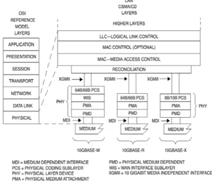
10-Gigabit Ethernet is similar to the MAC layer of previous Ethernet technologies. It uses the same Ethernet address and frame formats. It supports data rate of 10 Gb/s and lower, using pacing mechanism for rate adaptation and flow control. As shown in Figure 1 below, the physical layer of the 10 Gb/s standard is divided into a physical coding sub layer (PCS) and a medium-independent interface (PMD). The PCS layer has two variations. One option encodes each serial block of 64 bits into an encoded block of 66 bits. The other option encodes each serial block of 8 bits into an encoded of 10 bits. The work presented here addresses the 64b/66b version of PCS. For a comprehensive discussion of the 10 Gigabit standard, readers are referred to [13].
Fig 1. 10Gb/s Ethernet and Relationship with OSI Model
III.VERIFICATION ENVIRONMENT COMPONENTS
The Verification components are in effect mini verification environments. The primary objective is to reduce the effort required to construct and validate the complete verification environment. To be effective, verification components must be constructed as reusable, configurable environments which are packaged to be plug-and-play. The IEEE Ten Gigabit Ethernet standard describes a protocol and encapsulation methods for data communications. Two categories of verification components are required to verify the functionality of hardware devices that conform to this standard, and similar future standards:
• those that are not directly related to the standard but are useful for the creation and checking of data packets, and
• those that are required to emulate the behavior of hardware devices.
The first category includes components such as packet data generators, packet drivers, FIFOs (First-In-First-Out) and payload checkers. The second category includes components such as Ethernet framers, Ethernet deframers, CRC (Cyclic Redundancy Check) generators, payload scramblers and descramblers.
standard implementation. The components are designed to be modular and parameterizable so that they maybe reused in applications even outside the IEEE Ten Gigabit Ethernet standard. For example, the “raw packet generator” described in a later section is protocol-free in the sense that the data packets generated do not conform to any protocol such as Ethernet or HDLC. As such, it can be used in any environment where a data source is required.
The verification components implemented are fundamentally of two different types [14]:
• Time-consuming: this component is simulation time-aware. Typically, this means that the component is a driver or a receiver, which operates synchronously with respect to a clock. In addition, a component may operate asynchronously; for example, in response to an event such as an interrupt from the device-under-test (DUT).
• Non-time-consuming: this component does not have any notion of simulation time. Typically, this means that the component is a data source or a data sink and is activated by a task or function call from a time-consuming component.
The verification environment developed here consists of the following major components: Packet Generator; Payload Scrambler; Payload Descrambler; Cyclic Redundancy Check (CRC) Calculator; First-In-First-Out (FIFO) Buffers; Ethernet Framer; Ethernet Deframer; Packet Driver; Payload Checkers. For the sake of brevity, the functionality of only some of these components is described in the following subsections.
1. Packet Generator
In this work, the packet generator is designed as a parameterized Verilog module, that creates raw (no protocol associated) data packets, which are suitable for input to other blocks that implement protocol framing (such as Ethernet or HDLC framer, for example). The module also generates control outputs such as the Start Of Packet (SOP) and the End Of Packet (EOP). The options supported by this module are the packet ID, packet size, packet byte pattern, and the pattern of idle bytes between packets.
2. Ethernet Framer
This component acts as an Ethernet framer. It accepts raw data as input and produces Ethernet frames, which encapsulate the raw input data, as output. Two major operations make up the Ethernet framing process: Frame Delineation (preamble insertion, destination address insertion, source address insertion, payload length insertion, payload data insertion, CRC computation and insertion, End-of-Frame (EOF) insertion); and the PCS encoding. These operations are described below.
i. Frame Delineation
a. Preamble insertion: The 8-byte pattern 0xfb_55_55_55_55_55_55_d5
b. Destination Address insertion: The 6-byte MAC address of the intended recipient of the frame-in-progress is inserted into the outgoing frame.
c. Source Address insertion: The 6-byte MAC address of the source of the frame-in-progress is inserted into the outgoing frame.
d. Payload Length insertion: The 2-byte pattern 0x_MSB_LSB indicating the total length of the payload in the outgoing frame.
e. Payload Data insertion: The raw payload received from the higher-layer client is inserted in “FIFO order” into the outgoing frame.
f. CRC computation and insertion: The CRC32 pattern, calculated over all bytes of the payload (beginning with the destination address and ending with the last byte received from the higher-layer client), is inserted in MSB-first order into the outgoing frame g. EOF insertion: The one-byte control character,
0xfd is inserted into the outgoing byte stream to signal an end of frame.
ii. PCS encoding
a. 64B/66B coding: This process involves the mapping of control codes, such as start of frame and end of frame, into special block-codes described in [13]. Two steps are involved: first, the data is broken up into 64-bit blocks which are scrambled as described in the next section, and second, synchronization bits (01 for data blocks and 10 for blocks with control characters) are inserted in front of every 64-bit block. These synchronization bits are used by the frame receiver to reliably recover data blocks from the transmission medium.
b. Scrambling: The self-synchronous payload scrambler, X^58+X^39+1, is used to scramble the 64-bit data block (the synchronization bits are not scrambled). Since the scrambler is self-synchronous, it is not necessary to initialize the state of the register, except at power-on reset when it is initialized with the “all-ones” pattern.
3. Ethernet Deframer
i. PCS decoding
a. Detection of synchronization bits: As described in the previous section, every block of 66 consecutive data bits is guaranteed to contain two synchronization bits (01 in the case of data blocks and 10 in the case of blocks containing control codes). To correctly identify the location of these bits, the deframer uses the following algorithm :
i. A 66-bit shift register, called the framing window, is initialized with a pattern of all 1s. At any time, this register indicates whether the corresponding bit position in the incoming bitstream is a candidate for the location of synchronization bits (a 0 indicates no synchronization bits were found at this location, and a 1 indicates a potential location).
ii. Every bit position in a 66-bit block of incoming data is examined and if it does not match the synchronization bit pattern (01 or 10), the corresponding bit position in the framing window is cleared to indicate that this position is NOT a candidate for the location of synchronization bits.
iii. If the framing window has exactly one position where there is a ‘1’ and all other positions have ‘0’s, synchronization bits have been tentatively located, and the algorithm proceeds to step v. If the framing window has no locations with a ‘1’, the algorithm starts with step i. again. Otherwise, it proceeds to step iv. iv. After another block of 66 input bits
becomes available, steps ii. and iii. are repeated.
v. “N” 66-bit input blocks are examined to check whether the location of synchronization bits found earlier is still valid. “N” is a parameter that can be set to trade off speed against accuracy of location of synchronization bits. For instance, choosing a very large value of N increases the reliability of location of the synchronization bits. However, this also increases the time the deframer takes to “lock” onto the synchronization bits in the incoming bit stream, and therefore increases the delay between reset and actual recovery of data. If all N input blocks have the synchronization bits in the same location, the algorithm terminates. Otherwise, the algorithm restarts from step i.
b. Descrambling of data blocks: Once the synchronization bits have been reliably located, every block of 64 data bits sandwiched between the synchronization bits is recovered and descrambled using the X^58 + X^39 + 1 self-synchronous scrambler. The descrambled data bits are passed along to step 2 described below.
ii. Ethernet frame delineation
The raw payload (Ethernet frames) is extracted, from the descrambled byte stream resulting from the PCS Decoding step described previously, using the following algorithm:
a. The descrambled byte stream is examined for the location of the standard Ethernet preamble, 0xfb_55_55_55_55_55_55_d5. All data is ignored until a preamble is found. The preamble indicates the beginning of a data frame.
b. The destination and source addresses (48 bits each) appear in the byte stream immediately following the preamble
c. The two bytes following the destination and source addresses indicate the length (in bytes) of the current Ethernet frame. This length value is examined and any corrective action required, is taken. For example, if this value is too small, the current frame is discarded as a “runt” frame as described in the IEEE 802.3 standard.
d. All data bytes indicated by the length field (step c above) are recovered. The first data byte is indicated as the “start-of-packet” byte, and the last data byte is indicated as the “end-of-packet” byte.
e. After the end-of-packet byte, the inter-packet gap is examined. Normally, there should be an inter-packet gap of 12 bytes. However, up to 3 additional bytes (one extra gap byte per Ethernet frame) may be accumulated and a subsequent inter-packet gap may be less than 12 with an absolute minimum value of 9 occurring when the accumulated byte count reaches 3.
f. After the entire current frame is extracted and the inter-packet gap is found to be acceptable, the algorithm proceeds to step (a) above.
4. Packet Driver
The packet driver is a time-consuming component that communicates with the device-under-test (DUT) using the following: 8-bit data bus, bit data valid indicator, 1-bit start of packet (SOP) indicator, 1-1-bit end of packet (EOP) indicator 1-bit error indicator. In addition, the driver requires the following control inputs: a clock signal used to synchronize the outgoing data and a reset signal.
The driver includes one instance of the packet generator (described earlier). It is the responsibility of the parent module of this driver (usually, the top-level test bench) to set up all the necessary options in the driver as well as in the packet generator.
The data bus and the other control outputs (valid, SOP, EOP, err) are synchronized to the positive edges of the clock input. To prevent a race condition (where the DUT attempts to read the data bus while the data is not yet stable on the bus), the driver includes a small delay (a fraction of a nanosecond is sufficient) that is inserted between the positive edge of the clock and the time at which the data bus actually toggles. This guarantees that the data is stable at the next positive edge of the clock, and the DUT can sample the data bus at the positive clock edge without any problems.
A 1-bit “data valid” control signal is used to introduce randomness in the rate at which input is being sent into the DUT. For example, to make the byte stream “bursty,” this control signal can be set to 0 for multiple (randomly selected) cycles between packets. This creates inter-packet “gaps” which test the behavior of the DUT when presented with a bursty data stream. The DUT is expected to ignore all data bytes which are accompanied by a ‘0’ value on the “data valid” signal.
The 1-bit SOP and EOP signals are self-explanatory. These are used by a framer to insert standard headers and trailers in the outgoing (framed) data stream. The 1-bit error signal simulates a link error, for example, indicating an aborted packet transmission. When a DUT receives a packet marked as errored, some special action may be required, such as the appending of a special abort code. The 1-bit error signal is helpful in testing such features. For random testing, each of these control signals is independently varied randomly. It is expected that a well-implemented DUT would be able to handle all possible combinations of these signals, even those which violate protocol such as an SOP indication without a prior EOP or vice versa. In general, drivers and receivers (external to the DUT) are always active. As such, these drivers and receivers are not sensitive to DUT “reset.” However, this control input is provided to initialize statistical counts etc, to make it easier to implement test cases.
5. Payload Checker
This component implements a self-synchronizing byte comparator. It consists of two FIFO queues:
1. Expected queue: holds bytes produced by a model of the DUT being verified
2. Observed queue: holds bytes produced as output by the DUT.
In addition to the data bytes, some control information such as the “start of packet”, “end of packet” and “error status” is also enqueued in the expected and observed queues. This enables the accurate comparison of errored packets in addition to the clean packets.
Periodically, under the control of the test bench, the payload checker attempts to compare the data in the expected queue against the data in the observed queue. At the start of a typical test, the data at the head of the expected queue may not have corresponding data at the head of the observed queue since some data may be lost to the framing and synchronization operation. Therefore, the checker is in an “unsynchronized” state at the beginning of the test.
The checker achieves synchronization when it encounters data in the expected queue, which has corresponding data in the observed queue. When the checker finds a point of synchronization between the two queues, it flushes all data in the two queues that precedes the synchronization point in time. Once the checker is synchronized, all data is expected to match between the two queues. Unless the specific test case allows it, once the checker is synchronized, any mismatch between expected and observed data automatically indicates a failure. However, the checker can be optionally configured to resynchronize the expected and observed whenever synchronization is lost. This could happen, for example, when the DUT drops a packet but the model of the DUT does not. In some tests, this is acceptable, and the test case merely checks that all data exiting the DUT is correct.
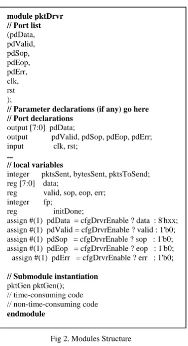
IV. COMPONENTS IMPLEMENTATION OVERVIEW
Fig 2. Modules Structure
Sections common to all verification components:
Port list: this is a list of all top-level inputs, outputs and bidirectional signals. For example, this list may contain signals such as a clock, reset, and data bus along with a data valid indication.
Parameter list: this is a list of all the configuration parameters that can be overridden at the time of instantiation of the component. For example, a data generator component may have an “Instance ID” which uniquely identifies each instance of this component. A data driver module that instantiates more than one copy of this generator would choose different “Instance IDs” for each instance.
Port declarations: this is a list describing the data type and bus-width of each signal in the port list described above.
Local storage declarations: this section contains all module-level state variables and signals, which are global to this component. In general, this section must be as small as possible since variables must be declared in the smallest enclosing scope. For example, the loop index variable in a for statement must be declared in the procedural block that contains the for statement. Specifically, this index variable must not be made global to the component since it increases the chance that this variable is inadvertently modified elsewhere in the component at run-time. This is possible since Verilog is a concurrent language and does support parallel execution of procedural blocks of code.
Sub-module instantiations: this section contains all sub-components that are instantiated in this component. Hierarchically, these sub-components are the “children” of this component. This section also contains any wire declarations necessary for hooking up the sub-components.
Time-consuming code: this section contains procedural code activated by one or more simulation time events such as the rising edge of a clock or the falling edge of an “active-low” reset signal. Usually, this code includes calls to non- time-consuming code described below.
Non-time-consuming code: this section typically consists of a collection of tasks and functions that help implement the component’s functionality. Each
component contains a task for setting the “default” configuration state of the component as well as a “state initialization” task to reset this component during a running simulation. Usually, tasks and functions are defined in a top- down fashion with respect to a static call graph. For example, if task A calls tasks B and C, the body of task A appears before the bodies of tasks B and C in the source code. Each section of the component is adequately commented describing the purpose of each variable and sub-component instance.
V. COMPONENTS VERIFICATION
This section describes sample experimental results obtained from detailed simulations of the verification components needed to verify the Ten Gigabit Ethernet standard. During simulation, several components generate log files that continuously record the input and output data along with additional information such as simulator time stamps. In addition, signal waveform databases are generated as well. These waveforms show the evolution of signals as a function of simulation time, and help in understanding and verifying the functionality implemented in each components.
Even though formal verification techniques have gained pace in the last few years, at present, simulation-based verification still remains the major techniques used to carry out RTL design verification. In accordance with the ‘correct-by-construction’ principle [15-16], the various components, developed in support of this work, are tested at the lowest level possible before being connected together at a higher level. For example, the packet generator and packet checker components are tested in the packet subsystem before being used in the framer subsystem. Two different subsystems are used to verify the correctness of the components developed: (a) the packet subsystem that verifies all packet-oriented components and (b) the framer subsystem that verifies all components.
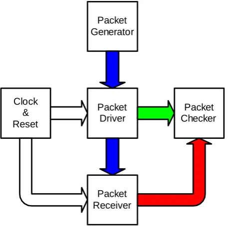
1. The Packet Subsystem
The packet subsystem is used to verify the correctness of the clock generator, reset generator, the behavioral FIFO, the packet generator, the packet driver, the packet receiver, and the packet checker. Figure 3 shows the layout and dataflow in the packet subsystem. The blue arrows show the primary data flow path. The green arrow
module pktDrvr // Port list (pdData, pdValid, pdSop, pdEop, pdErr, clk, rst );
// Parameter declarations (if any) go here // Port declarations
output [7:0] pdData;
output pdValid, pdSop, pdEop, pdErr; input clk, rst;
...
// local variables
integer pktsSent, bytesSent, pktsToSend; reg [7:0] data;
reg valid, sop, eop, err; integer fp;
reg initDone;
assign #(1) pdData = cfgDrvrEnable ? data : 8'hxx; assign #(1) pdValid = cfgDrvrEnable ? valid : 1'b0; assign #(1) pdSop = cfgDrvrEnable ? sop : 1'b0; assign #(1) pdEop = cfgDrvrEnable ? eop : 1'b0; assign #(1) pdErr = cfgDrvrEnable ? err : 1'b0;
denotes ‘expected’ data and the red arrow denotes ‘observed’ data. If all components function without any errors, the expected data matches the observed data. For brevity, the behavioral FIFO component is not shown in the figure. However, it is used by all components except the clock and reset generator. The clear arrows denote clock and reset signals used by the driver and receiver. The packet checker component works ‘asynchronously’ in the sense that its tasks and functions are invoked by the driver, receiver and the top-level test bench module.
Clock & Reset
Packet Driver
Packet Receiver
Packet Checker Packet
Generator
Fig 3. Packet Subsystem Test Environment Layout.
Figure 4 shows a subset of the signals in the test bench used to verify the functionality of the packet-oriented components. Of interest in this figure are the primary outputs of the packet driver component and the primary inputs of the packet receiver. As seen in the figure, the data transmitted by the packet driver is seen by the packet receiver one clock cycle later. Since the interface between the driver and receiver is one byte in width, the byte count signal increases by one every cycle.
As data flows through the subsystem, the ‘pktsSent’ variable (in the packet driver) and the ‘pktsSeen’ variable (in the packet receiver) increase until the test terminates. In Figure 4, these variables are shown incrementing from 14 to 15 at time marker 21,400. In this particular example, packets are being sent ‘back-to-back.’ In other words, there is no gap in time between the end of one packet and the start of the next (signals ‘pdEop’ and ‘pdSop’ in the driver).
Fig 4. Selected Packet Subsystem Signals
2. The Framer Subsystem
Figure 5 shows the layout of the test environment used to verify the correctness of the framer subsystem. The framer subsystem is tested only after the packet subsystem is demonstrated to be working without any errors. This approach ensures that any problems encountered while bringing up the framer subsystem are a result of errors in the framer and/or deframer blocks. Simulation runs are performed and various signals and log files contents were analyzed to verify the correctness of this module.
Packet Receiver
Packet Checker
Packet Driver Ethernet
Framer Ethernet Deframer
Packet Generator
Fig 5. Framer Subsystem Test Environment Layout
VI. TEST BENCH STRUCTURE AND FEATURES
Usually, the test bench also contains a behavioral model of the DUT written at a very high level of abstraction. The model used in this work is described using the Verilog HDL language [19]. This model receives the same input stimulus as the DUT, and generates the reference/golden output against which output from the DUT is compared. In addition to the DUT and the behavioral model, components such as clock generators and reset drivers are also contained in the test bench. Ideally, the test bench should centrally manage simulation control. What this means is that the test bench (actually, one or more procedural blocks inside the test bench) should control the activation and deactivation of drivers and receivers, event monitoring and error checking. This centralized control prevents contention and potential race conditions.
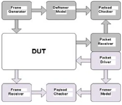
The structure and organization of the test bench must adequately reflect the flow of data as well as the hierarchy of the test bench elements. For example, in a test bench for a Ten Gigabit Ethernet framer, there should be a data source inside a data driver that generates raw data to be framed by the DUT. On the other side of the DUT, there must be a frame receiver that captures the data exiting the DUT and analyzes it for correctness. Before they are put together to verify the DUT, the individual verification components are tested separately for correctness. For example, in this work, the framer and deframer models are verified using their own test benches before they are integrated and used in a larger test environment. Figures 6 and 7 show two examples of this bottom-up strategy. It is important to note that both the framing and deframing modules are to be tested and verified separately. This is the reason for the two testing directions shown in the figures.
Fig 6. Test bench of the Framer verification component
Fig 7. Test bench of the Deframer verification component Figure 6 shows a test bench used to test the Framer and Deframer models. The Packet Generator creates raw data packets that are sent to the Framer Model, which
encapsulates these packets in Ethernet frames. These frames are passed along to the Deframer Model, which checks for frame structure and CRC correctness, extracts the packet data from each frame, and passes this packet data along to the Packet Checker. The Packet Generator also sends the data packets it generated to the Packet Checker as “expected data.” The Packet Checker compares the data packets received from the Packet Generator against the data packets received from the Deframer Model.
Figure 7 shows a test bench useful for self-testing the Deframer and Framer. The Frame Generator creates Ethernet frames that are sent to the Deframer Model, which checks for frame structure and CRC correctness, extracts the data packet in each frame, and passes packet data along to the Framer Model. The Framer Model encapsulates the data packets in Ethernet frames and sends these frames to the Frame Checker. The Frame Generator also sends the Ethernet frames it generated to the Frame Checker as “expected data.” The Frame Checker compares the frames received from the Frame Generator against the frames received from the Framer Model.
Figure 8 shows the organization of a test bench constructed by using the different verification components and modules implemented in this work. The Device-Under-Test (DUT) implements a framer/deframer pair that conforms to the IEEE Ten Gigabit Ethernet Standard. The DUT targeted by the verification components library described in this paper involves two parallel (duplex) data paths: one in the “transmit” direction and one in the “receive” direction. The large rectangle in the center labeled “DUT” depicts the device being verified. The two rectangles labeled “Framer Model” and “Deframer Model” predict the behavior of the DUT by producing the “expected output” and the payload checkers (one in each direction) verify that the expected output matches the data produced by the DUT.
Fig 8. Test Bench Organization
1. Transmit Data Path
packets are encapsulated in an Ethernet frame and passed along to the Frame Receiver. The Packet Driver also sends the packet data to the Framer Model, which implements the same functionality that is built in the DUT. The Payload Checker is used to compare the frames received from the DUT against the frames received from the Framer Model.
2. Receive Data Path
In the “receive” direction, the DUT receives frames generated by the Frame Generator. These frames are processed by the DUT for correctness of protocol and CRC, and packet data is extracted and passed along to the Packet Receiver. The Frame Generator also sends the same frames into the Deframer Model, which implements the same functionality that is in the DUT. The packet data extracted by the Deframer Model is sent to the Payload Checker. This data is compared against the packet data received from the DUT via the Packet Receiver. Each of the components of the test bench in Figure 8 instantiates other components from the verification library. For example, the packet driver instantiates the packet generator, and the payload checker instantiates two copies of the FIFO component and so on.
VII.CONCLUSION
The primary responsibility of a verification engineer or team of engineers is to create a full verification system in a reasonable amount of time and in a cost-efficient manner. Rather than developing and verifying the various components needed to verify the DUT, we advocate the presumption that having available a library of reusable verification components will no doubt assist in reducing the verification cycle. Reusing rather than developing module level verification components such as those typically used in the verification of network protocols and devices and discussed in this paper (frame generators, checkers, etc) can assist in assuring the module functional consistency and in reducing the efforts of checking the module under test. In time, enhancing features might be added to existing protocols or alternatively a newer version of a given protocol might need to be implemented as an ASIC; regardless, there are critical verification components similar to the ones discussed in this work that will continue to be used as part of the newer verification environment. The absence of these components would simply mean the engagement of the verification team in developing similar components, an effort that would simply elongate the design cycle.
In conclusion, a framework for the development and use of modular reusable verification components is discussed. By various published estimates, functional design verification constitutes up to approximately 70% of a typical design project’s time and effort budget. The paper discussed the design and implementation of reusable verification components using the IEEE Ten Gigabit Ethernet Standard (IEEE 802.3ae) as a case study. Reusable verification modules are built, tested and successfully used. The methodology proposed and the
verification components developed are transferrable across projects with minimal effort. Use of the techniques presented in this work is expected to reduce development time and expense, and result in more robust hardware devices.
REFERENCES
[1] J Bergeron, “Writing Testbenches: Functional Verification of HDL Models”, Kluwer Academic Publishers, 2000.
[2] M.K. You, Y. Oh, G. Song, “Implementation of a
Hardware Functional Verification System Using SystemC Infrastructure”, Proc. of TENCON 2009.
[3] V. Peris et. al, “Reuse Scenarion for VHDL-Based
Hardware Design Flow”, Proc. European Design Automation Conference, 1995.
[4] M. F. Jacome and H. P. Peixoto, “A Survey of Digital
Design Reuse”, IEEE Design and Test of Computers, May-June 2001.
[5] W. Savage et. al, “IP Reuse in the System on a Chip Era”, Proc. of the 13th IEEE International Symposium of System synthesis, 2000.
[6] Foster, , et al., “Principles of Verifiable RTL Design: A Functional Coding Style Supporting Verification Processes in Verilog”, Kluwer Academic Publishers, 2001.
[7] O. Petlin et al., “Methodology and Code Reuse in the
Verification of Telecommunications SoCs,” Proceedings of the 13th Annual IEEE International ASIC/SOC Conference, 2000.
[8] Y. Lu, “Design Verification Concepts,” Proceedings of the 4th International Conference on ASICs,” 2001.
[9] Verisity Corporation, “Verification Reuse Methodology,” White Paper available from company web site (www.verisity.com).
[10]Z. Kirshenbaum,“Verification Reuse Offers Real
Benefits,” EE Design Magazine, March 2001.
[11]T.L. Anderson, “Verification Reuse Enables Design
Reuse,” EE Times Magazine, December 2002.
[12]R. Yang, L. Wu, J. Guo, B. Liu, “The Research and
Implement of an Advanced Function Coverage Based Verification Environment”, Proceedings of the 7th International Conference on ASIC, 2007.
[13] IEEE Std. 802.3ae-2002 ( http://www.ieee802.org/). [14]S. Palnitkar, “Design Verification with E”, Prentice Hall
Publishers, 2003.
[15] M. Lloyd, “Correct-by-construction becoming design
mantra,” EE Times, November 2003.
[16]G.J, Milne, “Correct Hardware Design and Verification Methods”, Springer-Verlag Publishers, 1993.
[17]A. Sagahyroon, G. Lakkaraju, M. Karunaratne, “A
Functional Verification Environment”, Proceedings of the 48th Midwest Symposium on Circuits and Systems, 2005 [18] M.D. Ciletti, “Modeling, Synthesis and Rapid Prototyping
with the Verilog HDL”, Prentice Hall Publishers, 2003.
[19]Verilog HDL Language Reference Manual (LRM), Open
Verilog International (OVI), Inc. (http//www.accellera.org) [20]A. M. Bhavikatti, S. Kulkarni, “VHDL Modeling of Wi-Fi MAC Layer for Transmitters”, Proc. of the Advances in Computing Conference, 2009.
[21]T. Nguyen, M. Duregger, G. Pelz, “Full System
Verification of CAN Networks at High Speed Transmission Rates”, IEEE Behavioral Modeling and Simulation Workshop, 2009.
[22]J. Li, et al, “Embedded Architecture Description