FET
with
Underlap
Structure
for
Biosensing
Applications
Claris C. J. W1,2, M. K. Md Arshad1,2, C. Ibau1, R. Mat Ayub1, M. F. M Fathil1 and Norhaimi W. M. W2
1Institute of Nano Electronic Engineering, 2School of Microelectronic Engineering Universiti Malaysia Perlis, Kangar, Malaysia
ABSTRACT
This paper presents the numerical simulation of an underlap field effect transistor (FET) device architecture on silicon‐on‐insulator (SOI) substrate for biosensing applications. By using the Silvaco ATLAS device simulator, this work is aimed to elucidate the effects of the different gate lengths, the presence of interface charge on the underlap sensing region, and also the effects of different gate biases (i.e. singlegate biasing, synchronous doublegate biasing and asynchronous doublegate biasing) on the magnitude of drain current (ID) of the simulated device. It is found that shorter gate length with the positive charges (on the n‐p‐n structure), at the sensing channel area increased the electron concentration at the channel and substrate/buried oxide interface. In asynchronous doublegate with a +3V of back‐gate supply and synchronous double‐gate, both increased the ID at different magnitude level and off‐current. Thus, depending on the biomolecule charges, the substrate biasing can be altered to improve the device’s sensitivity.
Keywords: Underlap field‐effect transistor; biosensors; singlegate; synchronous doublegate ; asynchronous double‐gate biasing.
1.INTRODUCTION
A biosensor has an ability to transform physical or chemical changes as it accompanying biological reaction into an electrical signal. Typically, a biosensor has two elements, which are bio‐receptor and transducer. Bio‐receptor is an immobilized sensitive biological element that recognizes the analyte such as an enzyme, antibody and deoxyribonucleic acid (DNA). On the other hand, a transducer is used to convert the biochemical signal from the result of interaction between the analyte and bio‐receptor, into another form of readable signal. These variability of transduced signals are based on the concentration of analytes that is being detected in the solution [1], [2].
The semiconductor‐based biosensor configuration based on field‐effect transistor (FET) device is often used due to its powerful platform for the direct detection of biological and chemical species [3], [4]. FET‐based biosensors is claimed to have high scalability, mass reproducibility, and compatibility with the on‐chip integration on both the sensor and measurement system [5]. Various device architectures have been demonstrated at the device level [6], [7], [8]. In the so‐ called ion‐sensitive FET (ISFET) based biosensor, the metal gate of the FET is replaced by a bio‐ film layer material. Drain current is changing due to the bio‐modulated gate surface, known as the ‘gating effect’ that influences the channel conductivity of the device. ISFET biosensor offers an
110
outstanding architecture as compared to other devices in term of for use in high sensitive
measurements, portable instrumentation, easy operation with a small amount of sample, low cost with mass reproducible and high speed [9].
In order to overcome the problems of low binding probability in a carved nanogap and low structural stability which is stemming from the mechanically suspended nanogap structure, therefore the FET with underlap structure is used. Biomolecules in underlap structure showed a higher probability to bind with designed area [10]. Besides that, the channel potential is known to be very sensitive to external charges in the underlap structure. Therefore, the observation on current change can be done more precisely. The targeted molecules can be easily detected electrically by detecting the changes in the drain current [11]. Moreover, the combination of highly sensitive underlap FET structure with the presence of back‐gate biasing is expected to further enhance the sensitivity of the device since it can boosta low limit‐of‐detection (LOD) of the analyte molecules. With the implementation of double gate [12], [13],[14] it is argued that the sensitivity can be enhanced as demonstrated on device level [15].
In this paper, we simulate the underlap FET structure with a novelty of having an underlap as the transducing region for the bio‐molecular recognition site. The paper is expected to explain the significance of different gate length on the device’s electrical responses (I‐V), besides analyzing on the impact of singlegate, synchronous doublegate and asynchronous doublegate towards the electrical properties of the proposed device structure for biosensing applications.
2.METHODOLOGYONDEVICESIMULATION
2.1Device’sSubstrate
The simulations are carried out by utilizing ATLAS device simulation software. The device modelling structure is based on silicon‐on‐insulator (SOI) substrate with the thickness of the top p‐type silicon layer of 70 nm, the thickness of the buried oxide (BOx) layer of 145 nm, and the bottom bulk silicon substrate with 100 μm thick respectively [16]. This study is gravitated to use SOI as substrate because it is known as good electrostatic control for the transistor device channel. Adding to this, SOI has the ability to co‐integrate devices with other devices on silicon bulk by etching the top silicon layer and the underlying BOx layer. Fig. 1 illustrates the top view and side view of simulation device model with the presence of underlap region between the gate‐ drain terminals.
111
2.2DeviceModel’sDesigning
The top 70 nm silicon layer and bottom 100 µm silicon bulk were doping uniformly with p‐type
dopant at a concentration of 1x1015cm‐3. On the other hand, the source and drain regions were
doping uniformly with n‐type dopant at a concentration of 1x1020 cm‐3. The contacts were made
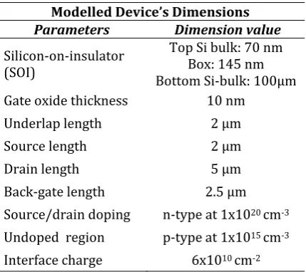
from aluminum with work‐function set at 4.6 electron‐volt (eV) layered on the contact surface, forming a Schottky contact on each of the terminals. The thickness of gate oxide was 10 nm with theunderlap length at 2 µm were positioning between the gate‐drain terminals. Following to this, the length of source and drain terminals were fixed at 2 µm and 5 µm respectively. These parameters were kept constant throughout the device modeling and simulations. Table 1 shows the fixed parameters on the modeled device for simulation.
Table1 Simulation device’s fixed parameters
ModelledDevice’sDimensions
Parameters Dimensionvalue
Silicon‐on‐insulator (SOI)
Top Si bulk: 70 nm Box: 145 nm Bottom Si‐bulk: 100µm Gate oxide thickness 10 nm
Underlap length 2 µm
Source length 2 µm
Drain length 5 µm
Back‐gate length 2.5 µm Source/drain doping n‐type at 1x1020 cm‐3 Undoped region p‐type at 1x1015 cm‐3 Interface charge 6x1010 cm‐2
The simulated gate lengths were 1 μm, 500 nm and 100 nm and have different interface charges, i.e. positive, negative and without interface charge on the underlap region. The interface charge were representing the biomolecule charges. For example, DNA always carries negative charge due to its negatively charged phosphate backbone, meanwhile, proteins can be either positively or negatively chargeddepending on its isoelectric point (pI). Later, these design parameters were simulating under the effect of singlegate biasing, synchronous doublegate biasing and asynchronous doublegate biasing to analyze the interactions between them. Table 2 shows the lists of simulation variables under test on the modeled device.
Table 2 Device’s Simulation Variables
ManipulativeVariables
Device’sdesignand
architectures Testedvariables
Interface charge on the underlap surface
Positive, negative and without interface
charge
Gate length 1 µm, 500 nm and 100 nm
Type of gate biasesSingle‐gate, synchronous doublegate and asynchronous doublegate with +3V
112
2.3Device’sSimulationParameters
For single‐gate, synchronous doublegate and asynchronous doublegate were biasing with the gate voltage at +1.5 V under voltage step of +0.02 V. However, the back gate terminal of the asynchronous doublegate was biasing at +3V under voltage step of +1.0V. The drain for all the three types of biasing was determined at +1.0 V under +0.1 V of voltage step.
3. RESULTSANDDISCUSSION
Fig. 2 shows the current – voltage (I‐V) characteristics for different gate length when the device is in single biased (only top‐gate is biased from 0 to 1.6 V). As claimed previously, the 500 nm gate length has a better performance with better trade‐off between on‐state and off‐state current, comparing to higher 1 μm and 100 nm gate length. The analysis indicates that a longer gate has a capability to introduce parasitic resistance between the source and drain terminals. This phenomenon has restricted the formation of inversion layer when the gate voltage was
applied, thus reducing the ID. While for 100 nm length, the gate is losing control of the channel,
thus increase the off‐state current. At this gate length, it forms a weak inversion region between the source and drain. As the gate length is reducing, the capacitive coupling of the channel potential to the source and drain increases relative to the gate, leading to significantly degraded short‐channel effects (SCE) which caused by the Drain‐Induced barrier lowering (DIBL). This happened due to impact of drain electric field during high drain voltage application when the potential barrier height for channel carriers at the edge of the source decreases [17].There is no current flow that has been detected when negative interface charge and no interface charge is applied to the surface of the underlap region.
Fig. 3 shows that the electron concentration along the channel when the underlap structure area has been subjected for different charges (positive, negative and no charge). Initially, the channel has doped with n‐type impurities. At the area underneath the channel region, the electron concentration changes from low to high concentration when the underlap is charging with positive and negative charges, respectively. Hence higher drain current can obtained the positive charge due to an increase of electron concentration at the channel. Therefore, the conducting layer of mobile electrons formed at the Si surface beneath the oxide has the ability to carry current between the source and drain, through the channel.
113
Figure3. (a) Tonyplot of the FET structure (b)Electron concentration along the channel.
Fig. 4 shows the current – voltage (I‐V) characteristics for different gate lengths graph when subjected to synchronous doublegate biasing. In synchronous doublegate, the front gate has connected with the back‐gate by utilizing only one voltage supply. We can see that, for 500 nm gate length with a synchronous doublegate and a positive interface charge at the sensing area
has significantly increased the ID compared to singlegate operation as discussed previously (Fig.
114
Figure4. The effect of different gate length with positive, negative and without interface charge at synchronous doublegate biasing.
Fig. 5 shows a graph of asynchronous double‐gate biasing. At this condition the back‐gate is supplied with +3 V voltage. Clearly at the expenses of high off‐state current, the increase of drain current is higher when single is being compared to synchronous doublegates.. This outcome occurs at all interface charges condition; i.e. positive, negative and no interface charge.
Figure5. The effect of different gate length with positive, negative and without interface charges of asynchronous double gate, Vbg = +3 V.
115
Figure6. Drain current characteristic for 500 nm gate length with singlegate, synchronous doublegate and asynchronous 3 V back‐gate biasing.
116
Figure7. Electron concentration for 500 nm gate length in different biasing along the terminals.
4.CONCLUSION
The simulated results on n‐p‐n junction, between source, channel and respectively, show that positive interface charge (which is translated into the positively charged biomolecules) has the highest drain current compared to the neutral and negatively charged molecules of the device. Among the three types of biasing, the asynchronous doublegate with +3V back‐gate supply has
generated the highest ID. From the simulated data, it shows that the presence of underlap
117
REFERENCES
[1] A. Koyun, E. Ahlatcıoğlu, and Y. K. İpek, “Biosensors and Their Principles,” A Roadmap
Biomed.Eng.Milestones, (2012)117.
[2] S. C. B. Gopinath et al., “Nanogapped impedimetric immunosensor for the detection of
16Â kDa heat shock protein against Mycobacterium tuberculosis,” Microchim. Acta, 183
(10) 2016.
[3] J. Y. Kim et al., “Surface engineering for enhancement of sensitivity in an underlap‐FET
biosensor by control of wettability,” Biosens.Bioelectron., 41(1) (2013) 867.
[4] M. F. M. Fathil etal., “Substrate‐Gate Coupling in ZnO‐FET Biosensor for Cardiac Troponin I
Detection,” SensorsActuatorsBChem., 242 (2016) 1142.
[5] J. Y. Kim et al., “An underlap channel‐embedded field‐effect transistor for biosensor
application in watery and dry environment,” IEEETrans.Nanotechnol., 11(2) (2012) 390.
[6] M. Gharayebi and A. Kh, “Fabrication and characterization of p‐type double gate and single
gate junctionles silicon nanowire transistor by atom microscopy nanolithography,” Int. J.
Nanoelectron.Mater., 7, 45–56 (2014) 45.
[7] O. C. Yee and L. S. King, “A comparative study of quantum gates and classical logic gates
implemented using Solid‐State Double‐Gate Nano‐MOSFETs,” Int. J.Nanoelectron.Mater.,
9, (2016)123.
[8] O. C. Yee and L. S. King, “Simulation Study of 2D Electron Density in Primed and Unprimed Subband Thin‐Body Double‐Gate Nano‐MOSFET of Three Different Thicknesses and Two
Temperature States,” Int.J.Nanoelectron.Mater., 9 (2016) 67.
[9] J. Park, H. Hiep, A. Woubit, and M. Kim, “Applications of Field‐Effect Transistor ( FET ) ‐
Type Biosensors,” Appl.Sci.Converg.Technol., 23(2) (2014) 61.
[10] R. Narang, M. Saxena and M. Gupta, “Superlattices and Microstructures Analysis of gate underlap channel double gate MOS transistor for electrical detection of bio‐molecules,”
SuperlatticesMicrostruct., 88 (2015) 225.
[11] K.‐W. Lee et al., “An underlap field‐effect transistor for electrical detection of influenza,”
Appl.Phys.Lett., 96(3) (2010) 33703.
[12] N. Othman, M. K. Md Arshad and S. N. Sabki, “Innovative Ground‐plane (GP) Architecture
for Thin Body and Thin Buried Oxide (UTBB) SOI MOSETs,” J.Nanoelectron.Optoelectron.,
12(7) (2017) 651.
[13] N. Othman, M. K. Arshad, and S. N. S. U. Hashim, “Impact of different ground planes of UTBB SOI MOSFETs under the single‐gate ( SG ) and double‐ gate ( DG ) operation mode,” in IEEEInter.ConferenceonSemiconductorElectronic, (2014) 88.
[14] N. Othman, M. K. Arshad, and S. N. Sabki, “Different Ground Plane ( GP ) Architectures on 25 nm Single‐Gate ( SG ) versus Double‐Gate ( DG ) UTBB SOI MOSFETs from Analog and
RF Perspectives,” J.Nanoelectron.Optoelectron., 12(2) (2017) 1.
[15] R. Adzhri etal., “High‐performance integrated field‐effect transistor‐based sensors,” Anal.
Chim.Acta, 917 (2016) 1.
[16] M. K. Md Arshad, N. Othman and U. Hashim, “Fully Depletion of Advanced Silicon on
Insulator MOSFETs,” Crit.Rev.SolidStateMater.Sci., (2015) 1.
[17] Z. Ramezani and A. A. Orouji, “Superlattices and Microstructures Investigation of veritcal