51
Influence of Adding SiC on Microstructure and Electrical
Properties of ZnO-based Nanocomposite Varistor
M. Azadmand
*1, A. Nemati
2, K. Arzani
1, N. Riahi Noori
3, T. Ebadzadeh
41- Department of Ceramic, Science and Research Branch, Islamic Azad University, Tehran, I. R. Iran
2- Materials Science & Engineering Department, Sharif University of Technology, Tehran, I. R. Iran
3- Niroo Research Institute, Ceramic & Polymer group, Tehran, I. R. Iran
4- Ceramic department materials and energy research center, Alborz, I. R. Iran.
(*) Corresponding author: [email protected]
(Received:15 Dec. 2013 and Accepted: 12 Jan. 2014)
Abstract:
In this research the influence of adding SiC on microstructure and electrical properties of ZnO-based Nanocomposite varistors were investigated. SiC was added with amounts of 10-0 mass% to ZnO-based varistor composition. It is found that SiC allows reaching to high threshold voltage with formation of fine-grained ZnO. Another important effect of adding SiC is formation Zn2SiO4 (Willemite) on the surface of SiC grains. With this effects SiC had great influence on Varistor electrical properties. On the other hand relative density decreased with increasing percentage of SiC in the composition. Hence with adding SiC to the composition, the threshold voltage of varistors (VT) and non-linear coefficient (α) increased at first and then decreased with increaseing of porosity. Also Current leakage decreased at first and then increased with adding more SiC. Also ZnO powder size effect on the final properties was examined in this reasearch by using submicron size and Nano size ZnO powder. The best achieved electrical result was threshold voltage as large as 4220 V/cm and non-linear coefficient α=44 that were gained by using of Nano ZnO powder and adding %4 SiC to the composition.
Keywords: Electrical properties, Grain growth, Nanocomposite, SiC, Varistor, ZnO.
Int. J. Nanosci. Nanotechnol., Vol. 10, No. 1, Mar. 2014, pp. 51-60
1. INTRODUCTION
Varistors (variable resistors) are voltage-dependent resistors with a symmetrical V/I characteristic curve whose resistance decreases with the increase of voltage. The voltage dependence of varistors or VDRs (voltage dependent resistors) may be approximately characterized by the formula
I = KVα (1)
Where K is constant and α denotes the non-linearity
exponent and in this way may be interpreted as a measure of the steepness of the V/I characteristic [1-2].
The first known ceramic material showing that
property is the silicon carbide (SiC). This ceramic
material consists of SiC particles (ranging from 50
to 100 μm in size), intimately bonded to a silica rich
vitreous matrix.
Single phase BeO doped SiC varistors was developed by hot isostatic pressing. Despite having superior electrical resistance than multiphase SiC
varistors, the ceramic’s non-linear coefficient remained low (α=5).
On the other hand high non-linear varistor materials
(α=50) were developed by Matsuoka. Those
other phases like the spinel (Zn7Sb2O12), pyrochlore (Zn2Bi3Sb3O14) and several polymorphic phases of bismuth oxide, distributed in the structure [3]. ZnO based varistors exhibit highly non-linear
current–voltage characteristics which find application in the field of protection gainst transient
voltage surges. In doped ZnO ceramics non-linearity
coefficients as high as α=70 can be achieved. In
standby, the varistor is subjected to a voltage below its characteristic breakdown voltage and only a leakage current pass through the bulk specimen. During transient surge the voltage between electrodes exceeds the breakdown voltage and the varistor becomes highly conductive diverting the current to ground and so protecting the circuit. The non-linear response originates on its polycrystalline microstructure and more
specifically on detailed processes occurring at the
grain/grain interfaces. By proper doping, the near grain boundary region becomes highly resistive while the grain interior turns into conductive, and electrostatic potential barriers build up at the grain boundaries due to charges being trapped at interface states [4].
In fact in Ceramic varistors based on the ZnO– Bi2O3–Sb2O3 system the characteristic non-linear current-voltage response is a consequence of their microstructure and electronic structure. Non-ohmic behavior is due to the presence of electrically active grain boundaries, formed by an intergranular Bi2O3 -rich phase that separates the semiconducting ZnO grains. Besides Bi2O3, other oxides enter in minor proportions into the varistor composition (Sb2O3, CoO, MnO2 and Cr2O3). Their role is to improve the electrical response [5].
With consideration that ZnO based varistors and SiC based varistors are used as two important generation of varistors, it seems that there is a vacant place in research papers to examine the properties of ZnO-SiC composite as a varistor. We know that SiC has a very strong covalent bond. As a tough material SiC can prevent the ZnO grain growth and help to have tinier microstructure. In
the present work, influence of amount of added
SiC and also affection of using Nano size ZnO
powder on microstructure, final density, and
current–voltage (I–V) characteristics of ZnO-based varistor ceramics has been investigated.
mass %
Composition Sb CoO PVA
2O3
Bi2O3 SiC ZnO 0.75 0.5 1.5 3 0 95 A 0.75 0.5 1.5 3 2 93 B 0.75 0.5 1.5 3 4 91 C 0.75 0.5 1.5 3 6 89 D 0.75 0.5 1.5 3 8 87 E 0.75 0.5 1.5 3 10 85 F
Table 1: Chemical composition of samples
53
2. EXPERIMENTAL
The basic formulation and preparing process in current research were chosen like conventional varistor formula and process. Analytical grades of ZnO (Zinchem, 300-900 nm), ZnO (Nano Amor,
20 nm), SiC-β (Nano Amor, 45-55 nm), Bi2O3 (Nano Amor, 90-210 nm), Sb2O3 (Nano Amor, 90-210 nm), CoO (Nano Amor, 90-90-210 nm), and PVA
(Sigma), were used in this work. SiC-β was chosen because mobility of SiC-β is higher than SiC-α and thus the electrical resistance of SiC-β is lower than SiC-α [6]. In this paper the samples which made by
Nano size ZnO powder are called Nano samples and the samples which made by Submicron size ZnO powder are called Submicron samples. The composition of the samples are shown in Table 1.
2.1. Sample preparation
The samples were prepared by conventional method. Table 1 shows the chemical compositions of samples prepared in this research. The oxide powders were weighed and then mixed during 20 min with Alumina balls and distilled water in fast mill. The Aqueous slurry obtained was dried in 80oC during 24 h. Then dry milling of the dried
batches was carried out during 20 min in fast mill without water just by alumina balls. The batches were molded in discs of 20 mm diameter and 3 mm in thickness under pressure of 100 Mpa by using hydraulic isostatic press. Then the green bodies were sintered at 1100oC for 1 h. The maximum
sintering temperature was chosen based on other researcher experiences [7-8].
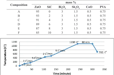
The rate of heating is shown in Figure 1. It was chosen with considering some physical and chemical reactions during the heating. Some of the important chemical reactions are as below [1, 9-10].
2.2. Density measurment and Analyzing of microstructure and phases
The density of the pellets was measured by Archimedes method.
ρ = Wd/ Ww- Ws (7)
%RD = (ρ/ ρth) × 100 (8)
Where ρ is density, Wd is dry weight, Ww is wet weight, Ws is soaking weight, ρth is theoretical
density that were measured for each composition, and %RD is relative density. To observe the microstructure scanning electron microscope (SEM, TESCAN-VEGII XMU, Czech) was utilized. In order to remove ZnO from surface and emerge grain boundaries, the pellets were polished and etched with 5 molar NaOH solution. Also the samples were coated with gold to be ready for SEM analyzing.
The crystalline phases were identified by an X-ray
diffractometer (STADI-MP, Germany) using 40
KV voltage and 30 mA amperage and Cu Kα as a
radiation source.
2.3. Measurement of V–I characteristics
For electrical varistor test, the pellets were polished and coated by conductive Carbon onto both faces with using conductive Carbon spray (KONTAKT CHEMIE, Belgium). For avoiding of surface current effect, the bodies were coated on the side part by an insulator epoxy resin. The I–V characteristics were measured at low currents until 10 mA under continuous voltage. The voltage–current (V–I) characteristics were measured by using a V–I source/measure unit. The nominal varistor voltages (VN) (breakdown voltage is the voltage at which the varistor switches from a highly resistive to a highly conductive state) at 1 and 10 mA and the threshold voltage VT (V/mm) (breakdown voltage/
54
unit thickness of varistor ceramic) were measured. VT=VN (1mA)/d, where d is the thickness of the
sample in mm) and the non-linear coefficient α (α=log(I10mA/I1mA)/log(V10mA/V1mA) =1/log (V10mA/ V1mA) according to the equation describing the V–I
non-linearity of the varistor ceramics I =KVα) were
determined. The leakage current (IL) (the current through the varistor in the pre-breakdown region of the V–I characteristic) was measured at 0.75 VN (1mA) [7].
3. RESULTS AND DISCUSSION
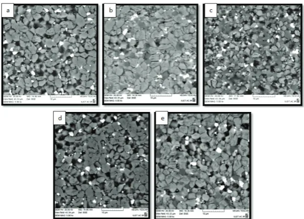
Six different varistor samples with different compositions were constructed. Figure 2 shows SEM micrographs of ceramic varistors sintered 1 h
in 1100˚C with 0, 2, and 6 mass% of SiC content.
As can be seen, basically, the growth of ZnO grains was prevented by SiC grains and therefore the average of ZnO grain sizes decreased as the amount of SiC increased. From the other point of
view, densification has been limited by increasing
the amount of SiC. With the increase of mass% of SiC from 0% up to 10 % in the composition, the
average of ZnO grain size decreased from 4 μm to 2 μm and the amount of porosity increased from 6%
up to 25%.
So it will have two different effects on the varistor properties: 1-decreasing ZnO grain size 2- increasing the amount of porosity. For investigation
of ZnO initial powder size effects on the final
microstructure of varistors, series of samples were prepared with using ZnO nano size powder with the same formula. As can be seen in Figure 2 the average of ZnO grains in the samples content nano ZnO didn’t have sensible difference to the samples which prepared by submicron size ZnO.
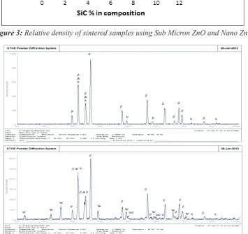
The increasing of porosity with adding SiC was
verified by measuring density. The density of
samples was measured by Archimedes method. The results are shown in Figure 3. It can be realized a sensible decrease in density of samples from 94% to 73% with the increasing amount of SiC from 0% to 10% in the composition. This event might be occurred by two reasons. Firstly SiC seeds as a physical barrier can prevent the ZnO grains to reach each other during the sintering. Hence SiC prevents
densification process. Secondly vaporization of
Carbon due to oxidation of SiC in high temperature can make porosities in the microstructure of samples. A similar rate of decreasing in density was occurred in nano samples. But nano samples revealed a higher density in comparison to submicron samples. In nano samples the average of relative density was about 2% higher than Submicron samples.
Figure 2: SEM image of varistor samples with different composition: (a) 0% SiC with submicron ZnO; (b) 2% SiC with submicron ZnO; (c) 6% SiC with submicron ZnO; (d) 0% SiC with nano size ZnO; (e) 2% SiC with nano ZnO
55
Several phases were identified by assisting EDX and
XRD analyses. XRD patterns of the investigated samples are given in Figure 4.
According to XRD peaks in the sample without
SiC, three phases were identified: ZnO phase as
the main phase, Zn7Sb2O12-type Spinel phase, Zn2Bi3Sb3O14 Pyrochlore phase. In samples which had SiC content ,moreover the mentioned phases, additional peaks were evident and their intensity
increased with the increasing of SiC amount in the starting composition .These phases were
identified as be SiC-β,and Willemite (Zn2SiO4). Willemite is created by combination ZnO and the layer of SiO2 on the surface of SiC grains. Due
to this fact that the SiC-β’s peaks were existed
in XRD patterns, so it can be say that there is
possibility of existing of remained SiC-β in the
core of Willemite phase.
Figure 3: Relative density of sintered samples using Sub Micron ZnO and Nano ZnO
Figure 4: XRD pattern of varistors with different composition (W: Willemite ,
P:Pyrochlore , Z:ZnO , S:Spinel, SiC: Silicon carbide): (a) 0% SiC; (b) 4% SiC
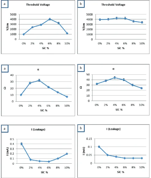
The likely position of willemite, SiC, and ZnO phases is shown in Figure 5. I-V electrical test of samples was carried out. Characteristic curves of varistor samples with six different amounts of SiC and two different ZnO grain sizes are depicted in Figure 6. As can be seen, all the samples showed varistor electrical behavior. Also threshold voltage,
α and current leakage of varistor samples were
displayed in Figure 7. The leakage current (IL) was measured at 0.75VN (at 1 mA).
Figure 5: Schematic image of likely position of
willemite, SiC, and ZnO phases in ZnO-SiC
based varistor
All the charts had an optimum point. As can be
seen the threshold voltage and α increased and then
decreased, and the current leakage decreased and then increased as the amount of SiC increased in the composition. Regarding to the SEM micrographs the increasing of SiC amount in the composition
will cause to decrease of final ZnO grain size.
Referring to equation 1, threshold voltage will increase if the ZnO grain Size decreases. So raising of SiC amount in varistor composition will cause to reduction of ZnO grain size and hence it will result in the threshold voltage rise.
VT = 3d/D (9)
Which VT : Threshold voltage, d: Varistor thickness, D: Average of ZnO grain sizes. Also based on the
final composition another likely reason for rising
the threshold voltage with the increasing of SiC amount can be mentioned. With consideration of XRD patterns it can be realized that by adding SiC in the varistor composition, a new phase that name is Willemite is created. Based on this fact that
57
Figure 7: Influence of adding SiC on threshold voltage, non-linear coefficient α, andcurrent leakage of varistor: (a) with using submicron ZnO; (b) with using nano ZnO
Willemite is a high electrical resistant phase with an electrical band gap as high as 5.5 ev [11], creation of this phase can cause to increase of threshold voltage.
On the other hand with continuance adding SiC, as it was shown in Figure 3 the density of samples decreased and it means the amount of porosity increased. So with continuance of adding SiC the amount of porosity increased and therefore the threshold voltage decreased. Also the non-linear
coefficient α was affected by adding SiC and the
Creation of Willemite on the surface of SiC grains is
the most likely reason of the increasing α by adding
SiC to the composition.
Willemite is created by combination ZnO and the layer of SiO2 on the surface of SiC grains. So the
final obtained microstructure will be a High resistant
phase (Willemite) between to semi conductor grains (ZnO & SiC) which is ideal for having a varistor
with high α. Morover the band gap of SiC is smaller
in comparicon to ZnO [12-13]. As like as threshold
voltage, non linear coefficient α decreased with
adding more SiC duo to increase of porosity. Also current leakage (IL) is affected by SiC amount. IL is the current which pass through the grain boundaries before threshold voltage.
With adding SiC, Willemite will be created in grain boundaries; and due to high electrical resistance of Willemite, current leakage decreases. With continuance of adding SiC, the amount of porosity will be increased and so it will cause to increase the current leakage. Regarding to the results the rate of the variation of electrical properties with SiC amount in Nano samples was lower than submicron samples. In addition, Nano samples
were shown higher threshold voltage, higher α, and
lower current leakage in comparison to submicron samples.
4- CONCLUSION
The influence of adding SiC to ZnO based varistor
on electrical and physical properties of varistor was investigated in this research. Regarding to the results, adding SiC to ZnO based varistor samples, decreased the ZnO grain growth process. So the
final structure of varistor was finer with using SiC
in the composition and it influenced on electrical
properties.
On the other hand there is another effect on varistor physical properties by adding SiC that is decreasing density. So these two different effects will cause
to different electrical behaviors. At first threshold voltage and α increased by adding SiC and then
decreased as the porosity increased. Also current
leakage decreased at first and then increased. The influence of ZnO grain size also was studied
in this work. Using Nano ZnO didn’t have sensible
effect on final grain size but it improved the equality
of microstructure and electrical properties. The best achieved electrical result was threshold voltage as
large as 4220 V/cm and non-linear coefficient α =44
that were gained by using of Nano ZnO powder and adding 4% SiC to the composition.
REFERENCES
1. M. Houabes: Corros. Sci., R. Metz, “Rare earth oxides effects on both the threshold voltage and energy absorption capability of ZnO varistors”, Journal of the Ceramics International., Vol. 33, (2006), pp. 1191–1197.
2. D. Xu, L. Shi: Corros. Sci., Z. Wu, Q. Zhong, X. Wu, “Microstructure and electrical properties of ZnO– Bi2O3-based varistor ceramics by different sintering
processes”, Journal of the European Ceramic Society., Vol. 29, (2009), pp. 1789–1794.
3. S.A. Pianaroa: Corros. Sci., P.R. Buenob, E. Longob, J.A. Varela, “Microstructure and electric properties of a SnO2 based varistor”, Journal of Ceramics
International., Vol. 25, (1999), pp. 1–6.
4. M. Peiteado: Corros. Sci., J. Fernandez, A. Caballero, “Varistors based in the ZnO–Bi2O3
system: Microstructure control and properties”, Journal of the European Ceramic Society., Vol. 27, (2007), pp. 3867–3872.
5. M. A. de la Rubia, M. Peiteado, J.F. Fernandez: Corros. Sci., A.C. Caballero, “Compact shape as a relevant parameter for sintering ZnO–Bi2O3 based varistors, “Journal of the European Ceramic Society., Vol. , (2004), 24. pp. 1212-1209.
6. G .Lynn Harris: Corros. Sci., “Properties of silicon carbide”, IET. ISBN 0-85296-870-1, (1995), pp. 170–180.
59
Vol. 36, (2009), pp. 1429-1437.
11. H. Chang: Corros. Sci., H. D. Park, K. S. Sohn, J. D. Lee, “Electronic Structure of Zn2SiO4 and Zn2SiO4:
Mn”, Journal of the Korean Physical Society, Vol. 34, No. 6, (1999), pp. 545-548.
12. A. Bakin, S. Andrey, “SiC materials and devices”,
World Scientific. ISBN 981-256-835-2, (2006),
pp. 43–76.
13. T. Ayalew, “SiC Semiconductor Devices Technolgy, Modeling, and Simulation”, Ph.D Thesis, Technical University of Vienna, (2010).
“Sintering process as relevant parameter for Bi2O3 vaporization from ZnO-Bi2O3-based varistor
ceramics”, Trans. Nonferrous metal. Soc.China., Vol. 19, (2009), pp. 1526-1532.
8. D. Xu, L. Shi: Corros. Sci., Z. Wu, Q. Zhong, X. Wu, “Microstructure and electrical properties of ZnO– Bi2O3-based varistor ceramics by different sintering
processes”, Journal of the European Ceramic Society., Vol. 29, (2009), pp. 1789–1794.
9. M. Lutful Arefin: Corros. Sci., F. rather, D. Dolejs,
A. Klimera, ”Phase formation during liquid phase sintering of ZnO ceramics”, Journal of ceramics international., Vol. 35, (2009), pp. 3313-3320. 10. F. Raether: Corros. Sci., M. Lutful Arefin, “Kinetic
field approach to study liquid phase sintering of ZnO
based ceramics”, Journal of ceramics international.,