Building Radio Frequency Transmitter for LTE User
Equipment
Marwa Mansour
Ain Shams UniversityCairo, Egypt
R.S. Ghoname
Faculty of EngineeringGirls’Campus
King Abdulaziz University, Jeddah Saudia Arabia
Electronics Research Institute, Cairo, Egypt
Abdelhalim Zekry
Ain Shams UniversityCairo, Egypt
ABSTRACT
Software defined radio implementation is required for LTE radio transceivers. An SDR consists of an RF front end and a digital processor platform DSP. This paper is devoted to the design and implementation of the front end which is divided into an active and a passive front end. The active front end consists of a frequency synthesizer, an I/Q modulator and an RF power amplifier while the passive front end includes the antenna and band pass filter. The paper presents the design, implementation, and testing of the LTE transmitter where the passive front end components are made of a microstrip circuits while the active components are selected from the off shelf components available in the semiconductor market.
For this, the antenna and filter were printed using FR-4 substrate material with dielectric constant of ɛr =4.4, thickness
of h = 1.6 mm and loss tangent tan δ = 0.025.
The frequency synthesizer is selected with step size of 200 KHz and frequency range from 0.37GHz to 5.7GHz, so that it covers all LTE bands.
The selected direct conversion I/Q modulator has frequency range from 0.2GHz to 6GHz. It allows direct modulation of an RF signal using differential baseband I and Q signals. The selected RF Power Amplifier has two modes of operation, a high power mode (HPM) and low power mode (LPM).The PA achieves gain of about 25.5 dB and 14.5 dB in HPM and LPM respectively over the 60 MHz bandwidth from 1920MHz to 1980MHz.
The performance of each component and the whole transmitter is measured using VNA (E8719A), EXA X-Series Signal Analyzer (N9010A), Agilent E8267D PSG Vector Signal Generator, and spectrum analyzer.
Keywords
LTE, SDR, RF transmitter, frequency synthesizer, IQ Modulator, PA,BPF,HPM, LPM, DGS, CST, Zeland IE3D, and VNA.
1.
INTRODUCTION
LTE was introduced in 3GPP. Its radio access is called evolved UMTS terrestrial radio access network (E-UTRAN). The air interface of E-UTRAN is based on orthogonal frequency division multiple access (OFDMA)in the downlink (DL), and single carrier frequency division multiple access (SC-FDMA) in the uplink (UL). The use of SC-FDMA in the uplink rather than OFDMA reduces the peak to average power ratio (PAPR) by 2~4 dB and mitigates the linearity
requirement, compared with worldwide interoperability for microwave access (WiMax) [1].
LTE can use QPSK, 16QAM or 64QAM modulation schemes, and can be either frequency division duplex (FDD) or time division duplex (TDD). It supports six different channel bandwidths: 1.4MHz, 3MHz, 5MHz, 10MHz, 15MHz, and 20MHz, which provides more deployment flexibility than previous systems.
There are several existing design and implementations that have been reported in the literature. Such as LTE transmitter for 3GPP is fabricated using 130nm RFCMOS in [2]. A prototype transmitter for LTE band 1 was developed in [3]. A design of LTE transmitter based on a polar PWM architecture is introduced in [4] but the system was not implemented. In this paper, according to our knowledge, it is the first time to introduce a design and implementation of the whole LTE RF transmitter which consists of frequency synthesizer, IQ modulator, power amplifier, band pass filter and antenna for LTE band 1 FDD or band 36 TDD.
In this paper attention will be paid to build a cellular multi-radio transmitter supporting cellular communication standards (WCDMA, HSDPA, HSUPA and LTE). Transmit bands addressed will be 1920 MHz to 1980 MHz band 1 FDD or band 36 TDD. To design such a transmitter, it is necessary to consider several parameters of the signal. Some parameters depend on the standard itself [5, 6] and so modulation schemes like bandwidth, power dynamics or envelope amplitude variations (also known as peak to average power ratio, PAPR). Other parameters directly depend on architecture like spectral purity, linearity or power efficiency The LTE transmitter can be divided into two major parts: baseband and RF. Typically, the baseband part is implemented digitally and the RF part is analog. A digital to analog converter (DAC) is connecting the Baseband and RF part.
The design must take into account the operating parameters of RF components, comprising the frequency synthesizer, IQ modulator, RF power amplifier, RF band-pass filter, and microstrip antenna.
2.
TRANSMITTER ARCHITECTURE
AND KEY REQUIREMENTS
In order to get out the specifications of the component of the transmitter, the architecture and the main performance parameters of the transmitter must be worked out. The direct up conversion transmit architecture shown in Figure 1 is becoming more common due to its low part count and power consumption. This transmitter architecture can be split into three different areas: digital baseband, analog baseband to RF and analog RF front-end. The main parts of the RF transmitter are the following:
1. Local oscillator (LO): that generates a CW signal of a frequency which, mixed with the input signal, produces a signal at the desired frequency. The signal produced by the LO is synchronized to the clock reference signal.
2. I/Q Modulator: that produces the RF signal by mixing the base band BB signal with the LO. 3. RF Power Amplifier: is a key part of the RF
front-end in any transmitter. PAs boost the signal power high enough such that it can propagate the required distance over the wireless medium [7].
4. Filter: A band pass filter is an important component that rejects the out of band signals.
5. Antenna: is a necessary component of every wireless communication system and provides a means for transmitting and receiving electromagnetic waves.
Fig 1: Classical direct conversion transmitter
LTE RF transmitter designers are facing very tough challenges. Here, elaborating on them from the following two perspectives: maximum linear output power and efficiency.
2.1
Maximum Output Power
The maximum linear power, Pmax, is the key specification for
the RF transmitter. Based on the 3GPP specification of LTE UE transmitter, there are four power classes defined. Currently, only class 3 is specified as 23dBm +/-2dB. To extract the maximum linear power requirements for the PAM, Eq.1 is used by counting the path loss budget PLoss and
the maximum power reduction (MPR).
(1)
MPR is used to address the peak to average power ratio PAPR variation due to the modulation scheme, location and the number of resource blocks (RB), which is the minimum unit of transmission and is 180 kHz wide and 0.5ms in duration. It is defined in Table 1.
Table 1. Maximum Power Reduction [8] Modulati
on
Channel bandwidth/ transmission bandwidth configuration (RB)
MPR (dB) 1.4 MH z 3.0 MH z 5 MH z 10 MH z 15 MHz 20 MH z
QPSK > 5 > 4 > 8 > 12 > 16 > 18 ≤ 1 16 QAM ≤ 5 ≤ 4 ≤ 8 ≤ 12 ≤ 16 ≤ 18 ≤ 1 16 QAM > 5 > 4 > 8 > 12 > 16 > 18 ≤ 2
Path loss budget depends on the application, transmitter front end architecture, duplex mode as well as frequency band. Usually, FDD path loss is higher than TDD. Also, in FDD, the frequency band with a narrower spacing between RX and TX has higher path loss. It is why the requirement of maximum power of Band II is higher than Band I.
When the PAM reaches the maximum power, it should still be linear, which means it's error vector modulation EVM and its adjacent channel leakage ratio (ACLR) is compliant with the specifications. LTE UE transmitter EVM requirement is shown in Table 2:
Table 2. EVM Requirement for LTE UE Transmitter [8]
Parameter Unit Level
QPSK % 17.5
16 QAM % 12.5
ACLR is another important linearity indicator. There are two ACLR measurements in LTE: E-UTRA_ACLR which uses LTE to LTE adjacent/alternate signal, and UTRA_ACLR which uses LTE to WCDMA adjacent/alternate signal. The limit -36dBc for UTRA_ACLR and -33dBc for E-UTRA_ACLR is often used.
2.2 Efficiency
In the LTE application scenarios, the current consumption is even more important than today’s voice centric devices. Yet, even with SC-FDMA, PAPR of LTE signal is still higher than WCDMA. For example, with a typical LTE signal with 10MHz, 12 Resource Blocks QPSK (MPR=0), its PAPR is approximately 2.8dB higher than WCDMA, Higher PAPR increases the required back off of output power and is expensive and modest in its efficiency.
For handset applications, higher efficiency means longer battery life. Focusing on the average talk mode current, Italk,
as a measurement of battery life. Italk is calculated as given in
Eq.2:
(2)
Where Itotal must include the sum of all currents and pdf is the
probability density function of the output power.
3.
ACTIVE FRONT END
3.1
Frequency Synthesizer
A frequency synthesizer is a device that generates a large number of precise frequencies from a single reference frequency [9].In the proposed LTE RF transmitter design; it is found that the LTC6946 is a suitable frequency synthesizer. The LTC6946 is a high performance, low noise, 5.7GHz phase-locked loop (PLL) with a fully integrated VCO, including a reference divider, phase-frequency detector (PFD) with phase-lock indicator, ultralow noise charge pump, integer feedback divider, and VCO output divider. The charge pump contains selectable high and low voltage clamps useful for VCO monitoring.
Figure 2 shows a simplified LTC6946 block diagram, along with the external reference clock and loop filter components. In a nutshell, the phase/frequency detector (PFD) compares the phase and frequency of the reference clock, fREF, after its
division by R to produce fPFD, to those of the VCO following
an integer division of N. The PFD then controls the current sources of the charge pump to ensure that the VCO runs at a rate such that when it is divided by N, its frequency is equal to fPFD and its phase is in sync with the reference clock. This
describes a negative feedback mechanism, with the external loop filter components stabilizing the loop and setting the control bandwidth. The O divider increases the output frequency range by dividing down the VCO output to create more frequency bands than just that of the VCO.
Fig 2: Simplified LTC6946 block diagram with external reference clock and loop filter [10]
3.1.1 Output Frequency
When the loop is locked, the frequency FVCO (in Hz) produced
at the output of the VCO is determined by the reference frequency, FREF, and the R and N divider values, given by
Equation 3:
(3) Here, the PFD frequency FPFD produced is given by the
following equation:
(4)
And FVCO may be alternatively expressed as:
The output frequency FRF produced at the output of the O
divider is given by Equation 5:
(5)
Using the above equations, the output frequency resolution FSTEP produced by a unit change in N is given by Equation 6:
(6)
To appreciate the simplicity of the design process with the LTC6946, a complete design for the LO of LTE RF transmitter is shown here. The design has the following frequency plan.
LO frequency band: 1920 MHz to 1980 MHz Frequency step size (channel-to-channel spacing):
20MHz
Reference clock frequency: 10 MHz
All further design choices can be made using the PLLWizard program.
Entering the given frequency information in PLLWizard and picking the approximate noise optimized loop bandwidth suggested by the PLLWizard tool produces the loop filter values needed to modify a DC1705B demo board. Since the LTC6946 VCO gain is nearly constant as a percentage of the frequency, the loop filter designed at any frequency within the band works for all other frequencies. Figure 3 shows a snapshot of PLLWizard used in completing this design.
(a) DC950 controller board and PLLWizard used in programming frequency synthesizer
(b) PLLWizard software tool.
Fig 3: Snapshot of the PLLWizard software tool used in designing a LO from 1920MHz to 1980MHz with 20MHz
The phase noise of the synthesized frequency as a function of the offset frequency from the center frequency is shown in figure 4. It is acceptable for LTE transmitter requirement.
Fig 4: Phase noise of the synthesizer output signal [10]
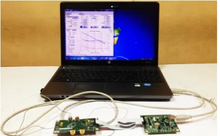
Figure 5 shows the frequency synthesizer measurement setup, where the frequency synthesizer board is connected to power supplies, spectrum analyzer, reference frequency, and connected to DC590 controller board.
Fig 5: Measurement equipment setup of LTC6946 frequency synthesizer
The spectrum output of the frequency synthesizer with a sinusoidal wave component 1.95 GHz and an output power level of -2.17 dBm is cleared in figure 6.
Fig 6: the measured LO output frequency at 1950MHz
3.2
The Direct Conversion I/Q Modulator
In the IQ modulator IQM the I part of the baseband signal is multiplied by a cosine carrier wave and the Q part is multiplied by a 90◦ shifted cosine carrier wave. In the proposed LTE RF transmitter the chip LTC5588-1 is selected as modulator. The LTC5588-1 is a direct conversion I/Q modulator designed for high performance wireless applications. It allows direct modulation of an RF signal using differential baseband I and Q signals. It supports LTE, GSM, EDGE, TD-SCDMA, CDMA, CDMA2000, W-CDMA, WiMax and other communication standards. Figure 7 shows a simplified LTC5588-1 block diagram.
Fig 7: 200MHz to 6000MHz Direct Conversion Transmitter Application [11]
The proposed I/Q modulator measurement setup is shown in figure 8, where I/Q modulator board is connected to power supply (3.15 - 3.45 V), spectrum analyzer, LO signal source adjusted at FLO of 1.95 GHz, and baseband signal source VCM
= 0.5V and modulating signal frequency of FBB = 100 KHz.
Figure 9 shows a photograph of IQ modulator (LTC5588-1).
Fig 8: Proper measurement equipment setup of LTC5588-1 I/Q modulator
Fig 9: A photograph of I/Q modulator (LTC5588-1)
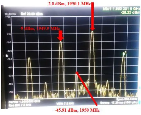
the image frequency at 1949.9 MHz is -8.6 dBm while the LO Feed through signal level at 1950 MHz is -45.91 dBm. It is apparent also from the frequency spectrum of the output signal that it contains second and third harmonics for the modulating signal with the third harmonics is much greater than the second harmonics.
Fig 10: The measured RF output on signal analyzer (EXA X-Series Signal Analyzer N9010A)
The RF output signal contain LO Leakage and an unwanted lower sideband image at LO-BB due to Amplitude and phase mismatches between I and Q signals
3.3
RF Power Amplifier
Power Amplifiers (PA) are a key part of the RF front-end in any transmitter. The chip RF7411 is selected for use in the proposed LTE RF transmitter. The RF7411 is a high-power, high-efficiency, linear power amplifier designed for use as the final RF amplifier in 3V, 50Ω WCDMA mobile cellular equipment and spread-spectrum systems. This PA is developed for UMTS Band 1 which operates in the 1920MHz to 1980MHz frequency band. Figure 11 shows the schematic of the evaluation board of power amplifier RF7411.
Fig 11: Evaluation board schematic of RF7411 [12]
The RF7411 has a digital control pin which enables a low power mode to reduce amplifier gain at lower power levels. The part also has an integrated directional coupler which eliminates the need for an external discrete coupler at the output. The RF7411 (Band 1) meets the spectral linearity requirements of High Speed Downlink Packet Access (HSDPA), High Speed Uplink Packet Access (HSUPA), and Long Term Evolution (LTE) data transmission. Because of its importance for the satisfactory operation of the transmitter intensive experimental validation of its performance parameters is carried out. The tests are introduced in the following sections:
3.3.1
DC Power Consumption
The DC power consumption is a major parameter in the PA. RF7411 operates from 3.2 V power supply and consumes about (3.2 V *0.4 A) 1.28 W at HPM and (3.2 V *0.116 A) 0.37W at LPM.
3.3.2
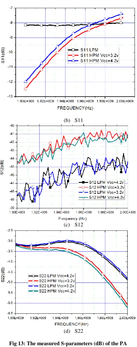
S-Parameters (dB)
RF7411 achieves power gain S21 14.5 – 25.5 dB over the 1920MHz - 1980MHz frequency band. Input return loss S11 is a measure of how close the actual input impedance of the circuit is to the nominal source impedance value usually 50 ohms. This PA achieves an input return loss S11 less than -8dB. Output return loss S22 is a measure of how close the actual output impedance of the circuit is to the nominal load impedance value usually 50 ohms. This PA achieves an output return loss S22, less than -3.5 ~-6.5dB. Reverse isolation S12 is the measure of transmission from output port to input port. It is required to prevent signal reflection from the output to the input in transmitter designs. This PA achieves a reverse isolation S12 less than -40 dB over the band from 1920MHz to 1980MHz. Figure 12 shows the measuring setup based on a network analyzer of the S- parameter of the amplifier. The measured S-parameters as a function of the operating frequency are shown in Figures 13.
Fig 12: A photograph of the measuring of the power amplifier (RF7411) using Vector Network Analyzer (VNA)
E8719A
(b) S11
(c) S12
(d) S22
Fig 13: The measured S-parameters (dB) of the PA (RF7411) (a) S21, (b) S11, (c) S12 and (d)S22
3.3.3
1dB compression point
The 1 dB compression point is an important requirement in RF power amplifier to avoid distortion. The input referred 1dB compression is defined as the input power level (in dBm) that causes the linear gain of the amplifier to drop by 1 dB. The output referred 1dB compression point (in dBm) is the sum of the gain of the amplifier (in dB) to the input referred 1dB compression point (in dBm). Consequently, the measured output 1dB compression point (Po, 1dB) is ~ 29
dBm at (1920-1980) MHz. Figure 14 shows the measured output power vs. input power.
Fig 14: The measured output power (dBm) vs. input power (dBm)
Figure 15 shows the measured drain efficiency, PAE, output power and gain vs. frequency when the input power is 5 dBm. Here, it is clearly shown that the output power and gain do not vary significantly in the entire bandwidth between 1920MHz and 1980MHz. Both the output power and gain are maintained around 29 dBm and 25 dB respectively. Furthermore, the average drain efficiency is about 60% and the average PAE is about 59%.
Fig 15: The measured drain efficiency, PAE, Pout and gain vs. frequency
4.
PASSIVE FRONT END
In the following section, the properties of the components of the passive front end will be outlined for completeness. The detailed description of such passive front end is given in [13]:
4.1
Parallel Coupled-line BPF with DGS
Fig 16: The geometry parallel coupled-line BPF with DGSs. (a) Top view (b) Bottom view
Fig 17: A photo of fabricated three-pole parallel coupled-line BPF with DGSs. (a) Top view. (b) Bottom view
Table 3. Geometric dimensions of the parallel coupled-line BPF with DGS
N
n
W
(mm)
S
n(mm)l
n(mm)1 and 4 1.78 0.9 11.55
2 and 3 2.1911 1.36 11.45
The simulation and measured results of BPF with DGS is shown in fig 18. The passband center frequency is 1.95 GHz with -3dB bandwidth of 80 MHz (4.1%).
Fig 18: The simulated and measured reflection and transmission coefficients of the parallel coupled-line BPF
with DGS
4.2
Patch antenna with slit and DGS
The geometry of the proposed antenna is shown in Fig 19 .It is rectangular patch with a slit Ls and large defected ground structure [13].The antenna was designed on FR4 epoxy substrate with the overall dimension of 39 * 37.5 mm2. By adding a narrow slit close to the radiating edges the operating frequency can be varied. The ground plane has been modified by reducing its length to 3 mm to increase the bandwidth and reduce the antenna dimensions. Table 4 illustrates the design values of the proposed antenna geometrical parameters.
(a) (b)
Fig 19: The geometry of the proposed antenna. (a) Top view (b) Bottom view
Table 4. Antenna Geometrical Parameters
Parameter Value (mm) parameter Value (mm)
W 37.5 LS 19.24
L 39.3 Yo 6.97
WP 33.93 Lg 3
LP 29.83 Wg 29.5
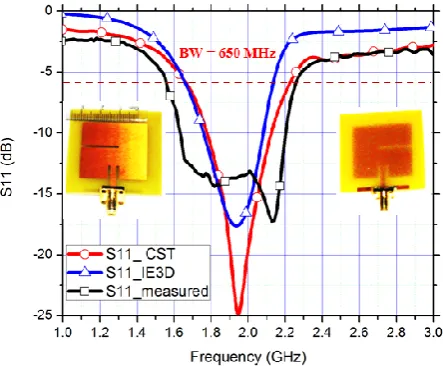
The antenna is fabricated and tested to validate the design and simulation results. The simulated and measured results of return loss for the first antenna are shown in Fig 20. From the results, it can be seen that the proposed antenna covers 650 MHz bandwidth from 1.58 GHz to 2.23 GHz. Hence, the proposed antenna can be used in this state in several wireless communication systems as LTE Bands 1, 2, 3, 4, 9, 10, 23, 25, 33, 34, 35, 36, 37, 39 [8, 15].
Fig 20: The measured and simulated return loss of the proposed antenna
5.
MEASUREMENT OF THE WHOLE
LTE RF TRANSMITTER
Fig 21: the proposed LTE transmitter
For testing the assembled RF transmitter, the main focus is on examining the characteristics of the components that may impact the quality of the transmitted RF signal, for example, errors in the IQ modulator such as IQ offset or gain imbalance, IQ timing misalignment, LO feedthrough, phase noise, and EVM as well as distortion characteristics such as ACLR and spectral regrowth.
Testing the transmitter chain will require using a digital or analog baseband signal from the signal generator to drive the I/Q inputs and a signal analyzer to measure the RF output. The measurement setups for RF transmitter are shown in Figure 22.
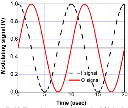
Fig 22: Measurement setups for RF transmitter The modulating signal must be analog IQ signal at frequency 100 KHz, CW, VP-P = 1V and common mode voltage VCM = 0.5 V. as shown in Figure 23.
Fig 23: The modulating signal I+ signal and Q+ signal
The LO is made to oscillate at frequency of 1950 MHz with amplitude 0dBm as shown in Figure 24.It is cleared that the phase noise equal -90dBc/KHz.
Fig 24: LO input signal wave form at 1950MHz, 0dBm, CW
5.1 DC power consumption
The DC power consumption is a major parameter of the RF transmitter. The RF transmitter with all its components draw a DC current of 0.7 A from a 3.3 V power supply. Then the overall power consumption of the transmitter = DC voltage * Current drawn from the supply = 3.3 v * 0.7 A = 2.31W
5.2 The RF output power
Figure 25 shows the measured output signal spectrum from the output of the amplifier with the transmitter assuming the IQ modulator a local oscillator signal given above. It is clear from the figure that the measured RF output power Pout at 1950.1 MHz = 27 dBm and The Image level at 1949.9MHz = -4dBm and the LO Feedthrough at 1950MHz =-27dBm.The unwanted components at the LO and image frequencies are due to baseband amplitude, offset and phase errors along with LO quadrature errors [16, 17].
5.3 Maximum output power
Effective isotropically radiated power (EIRP) is defined, as takes the antenna gain, Gant, into account. The EIRP is defined
as:
Fig 25: the measured RF spectrum of the output signal from LTE RF transmitter after the power amplifier
5.4 Dynamic range
By definition
5.5 Transmitter Efficiency
= 20.24%,
Which is much less than that of the power amplifier alone because the power consumption in the other component of the transmitter.
6.
CONCLUSION
The proposed LTE transmitter consists of active part and passive part. The passive elements are the antenna and filter. The antenna and filter are fabricated on FR4 substrate which is low cost. Firstly the size of the proposed antenna is smaller than the conventional patch antenna because of the partial ground. The size of the proposed antenna design reduced by 42.3% compared to the size of conventional patch antenna. The bandwidth of the proposed antenna is 0.65 GHz (1.58 - 2.2395 GHz).Secondly the proposed filter is a third order parallel couple filter with defected ground structure. With DGS the dimension of filter reduced from 84.4mm*21.8mm to 45 mm* 25 mm and the filter became more sharpness. The DGS band pass filter operates at center frequency 1.95 GHz and 3 dB frequency 80 MHz.
The active elements include the frequency synthesizer, IQ modulator and power amplifier. Each one of those real made components is selected to work in LTE bands.
The frequency synthesizer (LTC6946) operates in a wide frequency range from 0.37GHz to 5.7GHz so it covers all LTE bands. LTC6946 is programmed using PLLWizard program and DC590 controller board and its output is adjusted to 1.95 GHz.
The modulator (LTC5588-1) allows direct modulation of an RF signal using differential baseband I and Q signals. RF power amplifier (RF7411) has two mode of operation LPM and HPM as well as it has frequency band from 1920 to 1980MHz. The proposed PA operates from 3.2v power supply and consumes about 1.28 W. This PA achieves average power gain 25.5 dB, input return loss less than ~-10dB, output return loss less than -6.5 dB and reverse isolation less than -45dB.
Finally the whole LTE transmitter is gathered and tested and the measurements show that the transmitter response is the resultant of the responses of its components.
We succeeded to design, build and test a fully functioning LTE transmitter for user equipment.
It is found that such built transmitter can satisfy the requirements on the LTE front end for the user equipment.
In the future work the transmitter will be integrated in a single PCB board.
7.
ACKNOWLEDGMENTS
The article is partially supported by a grant of the Foundation of Computer Science, NY, USA.
8.
REFERENCES
[1] M. Rumney, LTE and the Evolution to 4G Wireless, Agilent Technology, (2009).
[2] Zhang Weifeng, Huang Jiwei, Wang Riyan, Fang Min, and Li Zhengping, “A 127mW SAW-less LTE
Transmitter with LC-load Bootstrapped Quadrature Voltage Modulator in 130nm RFCMOS ”, pp.2135-2138, IEEE, 2012.
[3] Takahiro Nakamura, Naoki Kitazawa, Kaoru Kohira, and Hiroki Ishikuro, “A SAW-Less LTE Transmitter with High-Linearity Modulator using BPF-Based I/Q Summing”, pp. 387-390, IEEE, 2014.
[4] Martha Liliana Suarez Penaloza, Václav Valenta, Geneviève Baudoin, , Martine Villegas, and Roman Maršálek, “High efficiency LTE transmitter considering a polar PWM architecture and RF front-end blocks”, Proceedings of the 3rd European Wireless Technology Conference, September 2010, Paris.
[5] LTE and WCDMA standard specifications: 3GPP TS 25.101 V9.1.0(2009-09).
[6] GSM / EDGE standard specifications: 3GPP TS 45.005 V8.3.0 (2008-11). 3rd Generation Partnership Project; Technical Specification Group GSM/EDGE; Radio Access Network; Radio transmission and reception (Release 8).
[7] P. Reynaert and M. Steyaert. RF Power Amplifiers for Mobile Communications. Ed. by M. Ismail. Springer, 2006.
[8] 3GPP TS 36.101-v9.4.0, E-UTRA user equipment radio transmission and reception.
[9] B. G. Goldberg, H. Eisenson, “Frequency Synthesizer Strategies for Wireless,” Microwave Journal, June 1993, 24, 26, 31, 34, 36, 39-40.
[10]Ultralow Noise and Spurious 0.37GHz to 6.39GHz Integer-N Synthesizer with Integrated VCO, Data Sheet, www.linear.com/LTC6946.
[11]200MHz to 6000MHz Quadrature Modulator with Ultrahigh OIP3, Data Sheet, www.linear.com/ LTC5588-1.
[12]3V WCDMA BAND 1 LINEAR PA MODULE, Data Sheet, www.linear.com.
[13]Marwa Mansour, Abdelhalim Zekry, and R.S. Ghoname, “A Passive Front End of Radio Transceivers for LTE Bands”, International Journal of Computer Applications (IJCA), vol. 114 – no. 8, pp.35-42, March 2015.
[14]J. S. Yun, J. S. Park, D. Ahn, “A design of the novel coupled-line band pass filter using defected ground structure with wide stopband performance,” IEEE Transaction on Microwave Theory and Techniques, Vol.50, No.9, pp.2037~2043, Sept. 2002.
[15]C. A. Balanis, Antenna theory, 3rd edition, John Wiley, New York, 2005.
[16]Henderson, B. C., “Predicting Intermodulation Suppression in Double-Balanced Mixers,” Watkins- Johnson Company Technical Notes. Vol. 10, No. 4, July/ August 1983.
![Table 2. EVM Requirement for LTE UE Transmitter [8] Parameter Unit Level](https://thumb-us.123doks.com/thumbv2/123dok_us/1257431.1631302/2.595.60.290.216.515/table-evm-requirement-lte-transmitter-parameter-unit-level.webp)