http://www.sciencepublishinggroup.com/j/ijssn doi: 10.11648/j.ijssn.20170502.11
Conference Paper
A Low Voltage Dynamic Synchronous DC-DC Buck
Converter
Benlafkih Abdessamad, Chafik Elidrissi Mohamed
Laboratory of Engineering Energy and Materials, Faculty of Sciences University Ibn Tofail, Kenitra, Morocco
Email address:
ab.benlafkih@gmail.com (B. Abdessamad)
To cite this article:
Benlafkih Abdessamad, Chafik Elidrissi Mohamed. A Low Voltage Dynamic Synchronous DC-DC Buck Converter. International Journal of Sensors and Sensor Networks. Vol. 5, No. 2, 2017, pp. 22-26. doi: 10.11648/j.ijssn.20170502.11
Received: May 21, 2017; Accepted: June 12, 2017; Published: July 18, 2017
Abstract:
This paper presents the design and modeling of synchronous DC-DC buck converter for device applications low consumption using Matlab/Simulink. In this work, the steady-state and average-value models for buck converter are analysed and it offers the modeled equations and simulation techniques of standard buck converter topology including variable loads. The goals of the designer are stabilized output voltage from a given input DC voltage using a Proportional Integral Derivative (PID) controller.Keywords:
Proportional Integral Derivative, DC-DC, Buck Converter, Matlab/Simulink, Controlled Converter1. Introduction
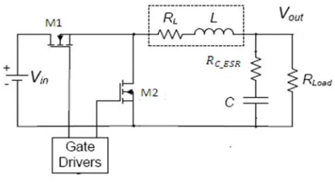
Current trends in consumer electronics demand progressively lower supply voltages due to the unprecedented growth and use of wireless appliances. Portable devices, such as laptop computers and personal communication devices require ultra-low power circuitry to enable longer battery operation. The key to reducing power consumption while maintaining computational throughput and quality of service is to use such systems at the lowest possible supply voltage. DC-DC buck converters [1-4] play an important role in modern Very-Large-Scale Integration (VLSI) system. Controller design for any system needs knowledge about system behavior [5-9]. Usually this involves a mathematical description of the relation among inputs to the process, state variables, and output. This description in the form of mathematical equations which describe behavior of the system (process) is called model of the system. This paper describes an efficient method to learn, analyze and simulation of power electronic converters, using system level nonlinear, and switched state- space models. The MATLAB/SIMULINK software package can be advantageously used to simulate power converters [10-13]. Figure 1 shows the basic topology of Synchronous DC-DC buck converter.
The paper is organized as follows. The synchronous buck converter is discussed and its key waveforms are presented in
Section 2. In Section 3, the analysis and development of the mathematical equations of the buck converter and their modeling under MATLAB/SIMULINK are presented. In Section 4, results of the converter and discussions are offered. Finally, the paper is concluded in Section 5.
Figure 1. Basic buck converter circuit.
2. Buck Steady-State Continuous
Conductions Mode Analysis
result is important because it shows how the output voltage depends on duty cycle and input voltage or, conversely, how the duty cycle can be calculated based on input voltage and output voltage. Steady-state implies that the input voltage, output voltage, output load current, and duty-cycle are fixed and not varying. Capital letters are generally given to variable names to indicate a steady-state quantity.
In continuous conduction mode, the buck power stage assumes two states per switching cycle [15, 16]. The ON state is when transistor MOS (M1) is ON and transistor MOS (M2) is OFF. The OFF state is when transistor MOS (M1) is OFF and transistor MOS (M2) is ON. A simple linear circuit can represent each of the two states where the switches in the circuit are replaced by their equivalent circuits during each state. The circuit diagram for each of the two states is shown in figure 2.
Figure 2. Buck power stage states.
The duration of the ON state is D T T where D is the duty cycle, set by the control circuit, expressed as a ratio of the switch ON time to the time of one complete switching cycle T. The duration of the OFF state is called T . Since there are only two states per switching cycle for continuous mode, T is equal to 1 D T. These times are shown along with the waveforms in figure 3.
Referring to figure 2, during the ON state, M1 presents a low resistance R ON , from its drain to source and has a small voltage drop of V I R ON . There is also a small voltage drop across the dc resistance of the inductor equal to I R . Thus, the input voltage V minus losses V I R is applied to the left-hand side of inductor L, M2 is OFF during this time. The voltage applied to the right hand side of L is simply the output voltage V , the inductor current I flows from the input source V through M1 and to the output capacitor and load resistor combination.
During the ON state, the voltage applied across the inductor is constant and equal to
V V V I R V
Figure 3. Continuous-mode buck power stage waveforms.
Adopting the polarity convention for the current I shown in figure 2, the inductor current increases as a result of the applied voltage. Also since the applied voltage is essentially constant, the inductor current increases linearly. This increase in inductor current during T is illustrated in figure 3. The amount that the inductor current increases can be calculated by using a version of the familiar relationship:
V L → ∆I ∆T
The inductor current increase during the ON state is given by:
∆I !"# $%&#' ( # )*+ T (1)
This quantity ∆I is referred to as the inductor ripple current.
Referring to figure 2 when M1 is OFF and M2 is ON, the voltage on the left-hand side of L becomes V , I R with -./, 0./ 12. The voltage applied to the right hand side of L is still the output voltage V . The inductor current I now flows from ground through M2 and to the output capacitor and load resistor combination.
During the OFF state, the magnitude of the voltage applied across the inductor is constant and equal to V V , I R . Maintaining our same polarity convention, this applied voltage is negative (or opposite in polarity from the applied voltage during the ON time). Hence, the inductor current decreases during the OFF time. Also, since the applied voltage is essentially constant, the inductor current decreases linearly. This decrease in inductor current during T is illustrated in figure 3.
The inductor current decrease during the OFF state is given by:
∆I )*+3 $%43' ( T (2)
∆I , during the ON time and the current decrease during the OFF time, ∆I , must be equal. Otherwise, the inductor current would have a net increase or decrease from cycle to cycle which would not be a steady state condition. Therefore,
these two equations (1) and (2) can be equated and solved for V to obtain the continuous conduction mode buck voltage conversion relationship.
Solving for -567:
V V V 89:
89:389;; V ,
89;;
89:389;; I R (3)
In addition, substituting T forT T , and using D 89:
8% and 1 <
=>??
=@ , the steady-state equation for
-567 is
V V V D V , 1 D I R (4)
A common simplification is to assume V , V , and R are small enough to ignore. Setting V , V , and R to zero, the above equation (4) simplifies considerably to:
V V D (5)
3. Simulink Model Construction of
DC-DC Buck Converter
3.1. Open Loop Modeling of DC-DC Buck Converter
The buck converter with switching devices will be considered here which is operating with the switching period of T and duty cycle D [17]. The state equations corresponding to the converter in continuous conduction mode (CCM) can be easily understood by applying Kirchhoff's voltage law on the loop containing the inductor and Kirchhoff's current law on
the node with the capacitor branch connected to it.
The ON state is when Switch (M1) is ON and Switch (M2) is OFF, the dynamics of the inductor current i t and the capacitor voltage vD t are given by equation (6).
E FGH
F7 2I -GJ -567 05J 02 K2L FMN
F7 O K2 K567
-567 0P/Q K2 K567 RO
(6)
The OFF state is when Switch (M1) is OFF and Switch (M2) is ON. The dynamics of the inductor current i t and the capacitor voltage vD t are given by equation (7).
E FGH
F7 2I-567 05J, 02 K2L
FMN
F7 O K2 K567
-567 0P/Q K2 K567 RO
(7)
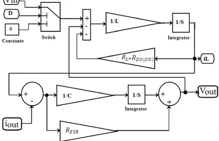
These equations (1) and (2) are implemented in Simulink as shown in figure 4 using multipliers, summing blocks, and gain blocks, and subsequently fed into two integrators to obtain the states i t and vD t [18-20].
Figure 4. Open –loop modeling of DC-DC buck converter.
3.2. Close-Loop Modeling of DC-DC Buck Converter
The PID controller has several important functions: it provides feedback; it has the ability to eliminate steady state offsets through integral action; it can anticipate the future
knowledge of the process dynamics they require. A PI controller is described by two parameters (Kp and Ki) and a PID controller by three or four parameters (Kp, Ki, Kd, and Ts). In these methods process dynamics are characterized by two parameters. One parameter is related to the process gain and the other describes how fast the process is. In the step response method, the parameters are simple characteristics obtained from the step response. In the frequency response method, the parameters are the ultimate gain and the ultimate frequency [22]. By tuning the three constants in the PID controller algorithm, the controller can provide control action designed for specific process requirements. The response of the controller can be described in terms of the responsiveness of the controller to an error, the degree to which the controller overshoots the set point and the degree of system oscillation [23].
The proportional, integral, and derivative terms are summed to calculate the output of the PID controller. Defining u(t) as the controller output, the final form of the PID algorithm is:
S T UVW T UGX W T YTZ7 UFF7FW T (8)
Figure 5 shows close loop modeling of DC-DC buck converter with PID controller.
Figure 5. Close –loop modeling of DC-DC buck converter with PID.
4. Results and Discussion
In this section, simulation results for synchronous buck converter circuit without controller and buck converter with PID controller. The results are based on output voltage rise time, peak time, and settling time. The simulation of the converter controlled with PID controller had been test with variation ranging from 0.5 Volt to 3.3 Volt.
Table 1 shows the specifications parameter of DC-DC synchronous buck converter.
Table 1. Buck converter parameter.
Parameters Values
Input Voltage 5 volt
Indutor 1µH
Capaitor 22 µF
Ron(M1)=Ron(M2) 300 mΩ
RL 20 mΩ
RESR 60 mΩ
Swithing Frequony 50 MHz
The simulation results of output voltage for buck converter with PID controller and without controller such as input voltage is 5 V are shown in following figures.
The simulation result of output voltage in figure 6 shows that the converter with PID controller lowers the input voltage (5V) to reference voltage (0.5V).
Figure 6. Output voltage when Vref set to 0.5 Volt.
In figure 7, the simulation result shows that the output voltage of the converter with PID controller go to 2 V (reference voltage value) from 5 V (input voltage).
Figure 7. Output voltage when Vref set to 2 Volt.
Figure 8. Output voltage when Vref set to 3.3 Volt.
5. Conclusion
This paper has provided a brief overview of the operation of a buck DC-DC converter, the mathematical model is derived from the system equations and provides an accurate
representation of the buck Converter. The
MATLAB/SIMULINK is also used for modeling and simulation of DC-DC converter.
As conclusion, the converter with PID Controller gives very good dynamic respond in order to achieve desired output voltage values for buck converter
Good behavior of the buck converter proves the robustness of the controller especially it shows good stabilization quality.
References
[1] Vahid Yousefzadeh, Dragan Maksimovic “Sensorless Optimization of Dead Times in DC–DC Converters With Synchronous Rectifiers”, IEEE TRANSACTIONS ON POWER ELECTRONICS, VOL. 21, NO. 4, JULY 2006. [2] M. Ordonez, M. T. Iqbal, and J. E. Quaicoe, “Selection of a
curved switching surface for buck converters” IEEE Trans. Power Electron., vol. 21, no. 4, pp. 1148–1153, Jul. 2006. [3] P. T. Krein, “Feasibility of geometric digital controls and
augmentation for ultrafast dc–dc converter response” in Proc. IEEE COMPEL, 2006, pp. 48–56.
[4] Yeong-Tsair LinMei-Chu JenWen-Yaw Chung “A monolithic buck DC–DC converter with on-chip PWM circuit”, Aug 2007, Microelectronics Journal.
[5] Vahid Yousefzadeh, Amir Babazadeh, Bhaskar Ramachandran, Eduard Alarcón, Pao and Dragan Maksimovic “Time-Optimal Digital Control for Synchronous Buck DC–DC Converters”, IEEE TRANSACTIONS ON POWER ELECTRONICS, VOL. 23, NO. 4, JULY 2008.
[6] P. Gupta and A. Patra, “Super-stable energy based switching control scheme for dc–dc buck converter circuits,” in Proc. IEEE ISCAS, 2005, vol. 4, pp. 3063–3066.
[7] K. K. S. Leung and H. S. H. Chung, “Derivation of a second-order switching surface in the boundary control of buck converters” IEEE Power Electron. Lett., vol. 20, no. 2, pp. 63– 67, Jun. 2004.
[8] C. Laorpacharapan and L. Y. Pao, “Shaped time-optimal
feedback control for disk-drive systems with back-electromotive force,” IEEE Trans. Magn., vol. 40, no. 1, pp. 85–96, Jan. 2004.
[9] K. Subramanian, V. K. Sarath Kumar, E. M. Saravanan, E. Dinesh “Improved One Cycle Control of DC-DC Buck Converter”, 2014 IEEE International Conference on Advanced Communication Control and Computing Technologies (ICACCCT).
[10] M. B. Sigalo, L. T. Osikibo “Design and Simulation of Dc-Dc Voltage Converters Using Matlab/Simulink” American Journal of Engineering Research (AJER) e-ISSN: 2320-0847 p-ISSN: 2320-0936Volume-5, Issue-2, pp-229-236, 2016.
[11] R. Ingudam, R. Nayak “Modelling and Performance Analysis of DC-DC Converters for PV Grid Connected System” International Journal of Science, Engineering and Technology Research (IJSETR), Volume 4, Issue 5, May 2015.
[12] Hanifi Guldemir “Study of Sliding Mode Control of Dc-Dc Buck Converter” Energy and Power Engineering, 2011, 3, 401-406 doi: 10.4236/epe.2011.34051 Published Online September 2011.
[13] Zhuo Bi, Wenbin Xia, “Modeling and Simulation of Dual-Mode DC/DC Buck Converter”, Second IEEE International Conference on Computer Modeling and Simulation, (ICCMS), pp. 371 -375, Jan 2010.
[14] K. S. Leung and H. S. H. Chung, “A comparative study of the boundary control of buck converters using first- and second-order switching surfaces -Part I: Continuous conduction mode,” in Proc. IEEE PESC, 2005, pp. 2133–2139. [15] Application Report Understanding buck power stages in switch
mode power supplies TI literature number slva057.
[16] R. W. Erickson, “Fundamentals of Power Electronics”, New York: Chapman and Hall, 1997.
[17] J. Mahdavi, A. Emadi, H. A. Toliyat, “Application of State Space Averaging Method to Sliding Mode Control of PWM DC/DC Converters”, IEEE Industry Applications Society October 1997.
[18] Vitor Femao Pires, Jose Fernando A. Silva, “Teaching Nonlinear Modeling, Simulation, and Control of Electronic Power Converters Using MATLAB/SIMULINK” IEEE Transactions on Education, vol. 45, no. 3, August 2002. [19] Juing-Huei Su, Jiann-Jong Chen, Dong-Shiuh Wu, “Learning
Feedback Controller Design of Switching Converters Via MATLAB/SIMULINK”, IEEE Transactions on Education, vol. 45, November 2002.
[20] Daniel Logue, Philip. T. Krein, “Simulation of Electric Machinery and Power Electronics Interfacing Using MATLAB/SIMULINK”, 7th Workshop Computer in Power Electronics, 2000, pp. 34-39.
[21] Aidan O‘Dwyer, “Handbook of PI and PID Controller Tuning Rules”, 3rd Edition, Imperial College Press 2009.
[22] Karl Johan Astrom and Tore Hagglund “PID controllers theory design and tuning” 2nd Edition, Instrument Society of America, 1995.