ISSN: 2231-5381
http://www.ijettjournal.org
Page 396
Design and Simulation of Microcontroller Based
Electronic Calendar Using Multisim Circuit Design
Software
Chukwunazo. J. Ezeofor
#1, Eric. C. Okafor
*2# Department of Electronic & Computer Engineering, University of Port Harcourt, Rivers State, Nigeria *Department of Computer Engineering, Enugu State University of Science & Technology, Enugu State, Nigeria
Abstract
-
This paper presents the design and simulation of Microcontroller based Electronic Calendar using Circuit design suite- MULTISIM. Paper calendar has been in existence and is used manually to keep date of each week of the month every year. The emergence of electronic calendar has taken precedence over the paper type. Every electronic device is now integrated with the electronic calendar to enable the user to keep time and date anywhere at any time. This report would enable user to understand the foundational design of the electronic calendar through simulation. The system design was achieved by dividing it into five modules namely power supply, 8051 control system, select and set, day and date, digital clock display. Digit numbers that represent time, date, month, and year were written in assembly language and tested. The simulated system displays accurate time of the day, day of the week, its date, month and year. 8051 Microcontroller controls every unit and the result is shown to the user through seven segments display.Keywords- 8051 Microcontroller, EPROM, Assembler, Programming Machine, Latch, decoder, seven segment display, LEDs, Transistor, Resistor.
I. INTRODUCTION
A
Microcontroller
based
Electronic
Calendar (MBEC) is a system that provides
accurate time, day and date of each day in a week
for many years to the user. The control unit of this
system is 8051 Microcontroller through which
every other unit is controlled. An oscillator that
clocks the 8051 is externally interfaced and
operates at 10.2MHz [1]. The system is divided into
different units and all work in hand to ensure its
accuracy and efficiency. Each sub-units of the
system namely date, day, and Select/set units are
controlled by 8051 microcontroller with sequence
of instructions that direct its performance. Every
coded digital number used is generated in
hexadecimal form and stored in the Erasable
Programmable Read Only Memory (EPROM). The
functional units made up of integrated circuits are
well interface to give its working ability. The
system architecture block diagram is shown in fig. 1.
The main aim of this work is to design and simulate electronic calendar with 12 hours digital clock of the year. The user can select and set any day, date and time of the day to the system and it would pick from the inputs [2]. The Light emitting diode (LED) and seven segments display would be used to display the days of the week (Monday through Saturday), date and time of the year.
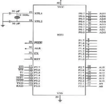
A. A. 8051 Microcontroller
The 8051 Microcontroller incorporates all the features that are found in microprocessor. The microcontroller has built in Read Only Memory, Random Access Memory, Input Output ports, Serial Port, timers, interrupts and clock circuit [3]. A microcontroller is an entire computer manufactured on a single chip, usually dedicated devices embedded within an application. The pin configuration is shown in fig.2.
O/P
Fig. 1: 8051 MBEC block diagram I/P
Power Supply Unit +5V
8051 Microcontroller
Control System Select and set buttons Unit
Digital clock display Unit
Sunday Monday Tuesday Wednesday Thursday Friday Saturday
Date Month Year
ISSN: 2231-5381
http://www.ijettjournal.org
Page 397
II. RELATED WORKThe related researched works are not limited to: a.Real Time Vehicle Locking and Tracking System using
GSM and GPS Technology-An Anti-theft System by Pravada P. Wankhade and Prof. S.O. Dahad (2011) which deals with the design & development of a theft control system for an automobile being used to prevent/control the theft of a vehicle. The developed system makes use of an embedded system based on Global System for Mobile communication (GSM) technology [3].
b.Design and program multi-processor platform for high-performance embedded processing by Yijun Liu, Zhenkun Li (2009) which addresses the issues of supporting parallelization in asymmetric multiprocessor (AMP) environment from both hardware and software sides, including cache coherence, semaphore and embedded software programming [4].
c. Remote Controlling of Home Appliances using Mobile
Telephony by Rifat Shahriyar, Enamul Hoque, S.M. Sohan, Iftekhar Naim, Md. Mostafa Akbar & Masud Karim Khan (2008) introduced a new mechanism so that the ordinary services of the mobile phones can be leveraged to communicate with and control the home appliances and make our homes a really smart one.
III. METHODOLOGY
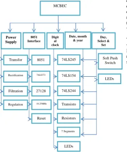
The design and simulation of MCBEC followed the flow chart diagram shown in fig.3.
MCBEC system involves five functional units. The System Design and Simulation approach used is Top-down hierarchical. The design focuses attention mainly on module integration and interface of the system. The system architecture has different integration units and each unit requires input to generates desired output.
A. Power Supply Unit
Power supply is a device that powers all the chips and components used in the design. The system requires a +5V Direct Current (DC) supply as the operating voltage for the 8051 microcontroller unit, integrated circuit, and seven segments display. This was achieved by designing different stages that makes +5V DC power supply.
1) Transformer:
Transformer is an electromagnetic device that accepts an alternating voltage and current and step down the voltage to the required value when plugged to 220-240 Alternating Current (AC) mains. The step down transformer is used because the voltage needed to power the circuit is very small to compare with the supply 220V. The 12V/500mA conventional step down transformer is used to capture 12V from 220V AC.
2) Rectification:
Rectification converts AC voltage into DC voltage and is achieved using full bridged diode. Bridged rectification gives full wave and was used to get positive voltage controlled circuit (VCC) and negative ground (GND) polarization.
3) Filtration:
The DC noise signals left after rectification is filtered using electrolytic capacitor in order to remove them totally in the circuit. The value of the capacitor used was chosen depending on the number of ripples and current that would appear at the output. The higher the value of the capacitor, more ripples is reduced. The voltage of the capacitor must be greater than the transformer voltage in order to avoid damage by higher voltage.
4) Regulation Stage:
This stage regulates the incoming voltage to a constant voltage depending on the required voltage. The three terminal Integrated Circuit (IC) regulator used is 7805 because +5V is required to power the Transistor Transistor Logic (TTL). The simulation circuit diagram is shown in fig.4.
Power Supply
8051 Interface
Digit al clock
Date, month & year
Day, Select &
Set
Transfor mer
Rectification
Filtration
Regulation
8051
74LS373
27128
10.25MHz
MCBEC
Reset
74LS245
74LS154
74LS244
Transisto rs
Resistors
Soft Push Switch
7 Segments
LEDs
LEDs
Fig. 3: MCBEC flow chart Block
ISSN: 2231-5381
http://www.ijettjournal.org
Page 398
B. How Power supply module works?
When AC cord is plugged into the 230V mains voltage (Nigerian AC Voltage rating) and the power supply switch (Ps1) switched ON, The voltage is transferred to the transformer primary coil. The transformer steps down the voltage from 220V to 12V. In order to convert the 12V AC into 12V DC, rectification is deployed which involves full bridged diodes. At this time, the signals from the transformer secondary coil possess some ripples. Filtration is required to remove the ripples and Electrolytic capacitor was used to achieve that. Also, since +5V DC is needed to power the ICs, 7805 regulator is used which maintains the steady positive voltage to the circuit.
C. Microcontroller interface with Memory
The Microcontroller interface consists of three ICs namely 8051, Latch 74LS373 and EPROM 27128.
1) 8051 IC Interface:
The 8051 controls all the activities that take place within the circuit board using sequence of written instructions.
2) LATCH 74LS373 interface:
The LATCH device interfaced 8051 and Erasable Programmable Read Only Memory (EPROM 27128). It de-multiplexes lower address lines (A0-A7) from the data lines (D0-D7) of 8051 when 8051 requests to send/receive data from EPROM 27128 with a specified address.
3) EPROM 27128 interface:
The EPROM 27128 is used to store written codes in either assembly language or c language that 8051 needs during its processing and execution time. Some 8051 have inbuilt memory and others are interfaced if the internal memory space is not enough to contain the programs.
D.How 8051 Communicate with EPROM 27128
The 8051 sends out address of memory location say 0AFH since it has 16 bits address lines on the address bus A0 to A15; strobes logic 1 from ALE in order to clock the latch to
de-multiplex lower address lines A0-A7 from data lines D0-D7. Also, 8051 strobes out logic 0 from PSEN (known as program store enable) read data located in the EPROM pointed at by the address sent from microcontroller. The data O0-O7 is send back to 8051 through data bus. When it gets to 8051, it decodes before taking any action. The process continues until the power is switched off. The soft push switch is used to reset the 8051 when needed to start at the beginning. When the button is pressed, 8051 reset its address 00h and start all over again. 10.25 MHz crystal oscillator located on pins 18 and 19 is used to provide time that clock 8051 during operation as shown in fig.5.
E. Digital Clock
This module has four stages namely: Buffer (74LS245 & 74LS244), 4-of-16 decoder/de-multiplexer (74LS154), PNP Transistors (BC327) and seven segment displays (common Anode).
1)Buffer Stage: Since the current produced by the 8051 would not be sufficient to drive many light emitting diodes used but need to be amplify in order to light all the seven segment display. 74LS245 and 74LS244 are used to amplify the currents in order to light many SSDs used as shown in the fig.6 simulation circuit diagram.
2)Decoder Stage: This stage decodes the input lines A0-A3 and selects the output line corresponding to the bits.
3) Transistors stage: This stage switches on the seven segment display when triggered. With the help of transistors, 8051 can select any seven segment display (SSD) device and display digital numbers. There are 16 transistors used for switching purposes.
4) Seven Segment display (SSD-Common Anode): The component is used to display digit numbers in the form the Fig.5: 8051 interface with EPROM27128
ISSN: 2231-5381
http://www.ijettjournal.org
Page 399
user would understand. Also the resistors connected are used to reduce the amount of current entering any component (load) placed after them. With resistors, LEDs and SSDs operation mode is assured. They would lights ON for hours without being damaged.
F. How digital clock module works
When the circuit is switched ON, the first display on the four SSDs would be 01:00 (the program default set point for time). 01 represents hours, (:) represents seconds and 00 represents minutes which signifies 1pm dot. The second (:) starts to counts immediately the switch is ON. The user is provided with soft push button to select and set the correct time at any moment if not correct. It follows the counting process of our time and the output is seen on the SSD meant for the hours. The data for the digit numbers are sent by the 8051 through (P1.0-P1.7) which were stored in the EPROM. The execution is done step-by-step according to the instructions and the simulation diagram shown in fig.6.
G. Date, Month and Year Unit
This module contains 8 seven segment displays and
8 PNP transistors. The arrangement is shown in fig.7 and other components used like buffers, decoder and resistors were shown in the design and simulation environment properly.
H.How the module works?
When the system is switched ON, the first display would be 01:01: 2014 and the user can select and set to current date using the select and set buttons provided. It displays date in digit, month in digit and year in digit everyday. The new date changes immediately 12:00am dot mid night clocks according to the program format. It also considered leap year every four years to ensure that the February date count from 1 to 29 instead of 1 to 28 as shown in fig.7.
I. Day
It comprises of 7 light emitting diodes (LEDs) that represents Sunday through Saturday. Buffers, decoders, transistors and resistors are also used in the design to achieve desired output.
J. How DAY module works?
When the system is switched ON, the default LED that represents Sunday of that week would lights ON and can be set to correspond with the date of that particular day. Each day, the LEDs responsible for that day would lights ON and stay ON until the time for that day elapse. It then changes to the next day LED when the proper time clocks. The process continues until the system is switched off. The simulation diagram for the day is shown in fig.8.
K. Select & Set Panel
This module comprises of two stages namely: Select and set buttons including LEDs for date, month, year, hour, minutes, and day. Two soft push switches are used to select and set any digit number as needed by the user. Pressing any switch interrupts the 8051 and must service the interrupt before preceding its normal operation.
Fig.7: Date, Month and Year module
Fig.8: Day Module of the Project
ISSN: 2231-5381
http://www.ijettjournal.org
Page 400
L. How the select & set module works
The select and set button is used to select and set LED corresponding to either date, month, year, hour, minute or day and enable any selected device to function as the user desired input/staring point. After the settings, the 8051 takes the new input value and activate the system to start from it. The simulation diagram is shown in fig.9.
IV.RESULTANDDISCUSSION
The design and simulation of the MCBEC was carried out using Electronic design simulation software called Circuit design suite (Multisim) pioneered by National Instrument. Firstly, power supply module was designed and simulated to ensure accurate +5V DC output is achieved. Secondly, 8051 Microcontroller interface to latch and memory was designed, linked to power supply and then tested. Thirdly, the program module of the digital clock display was written and tested gradually. Indicators for seconds, seven segment displays responsible for minutes, hours and LEDs for the day of the week were programmed and tested for accuracy. Any bugs found during testing were corrected. The program that interrupts the system and causes it to transfer control is written and tested. Other modules that work in hand with this module are also checked to ensure that the expected result was achieved successfully. The expected result was achieved starting from digital clock, day, date, month, and year as seen on the simulation display. The date, month, and year display every 24 hours which is expected from the specification. Indicators for Sunday through Saturday lights ON accordingly. The select and set buttons perform their functions properly. Therefore the actual result needed is achieved.
V. CONCLUSION
Microcontroller based electronic calendar is a device that help individual, company etc. at all level to keep time, date, month, and year. It consists of five modules namely power supply, 8051 interface, digital clock, data, month and year, select set and day. Each module has roles to play in the circuit to ensure the objective is met. All key modules of this work were carefully designed and simulated. After designing each key module, the program was written in assembly language and tested to ensure that the module is responding to the desired output on the display panel.
ACKNOWLEDGMENT
I would like to express my deepest appreciation to God for making this paper a reality. To my able supervisor, Prof Okafor Eric for all his advise and corrections. Special thanks to my family for all their moral and financial support throughout the research work. Also, to IJETT editors for had prepared this wonderful template, their commitment and prompt response in attending to journal papers.
REFERENCES
[1] M. Mamun and Z. Karim A.H,”Designing a Microcontroller based Smart Multi Language Learning Word Master”, in International journal of Engineering Science & Technology (IJEST), Vol. 3 No 1 Jan 2011,pp 84-88.
[2] R.J Tocci,“Digital system: principle and application, 4th edition, prentice
Hall inc….new Jerscy (1988) Pp 200-257
[3] A.S.H. Alsadi, “The development of embedded GPS-GSM based real time vehicle tracking”, Engineering and Technology Journal, 31(10), 2013, 1982-1999
[4] P. T. Tun, “Development and implementation of microcontroller-based digital clock,” World Academy of Science, Engineering and
Technology, Singapore. vol. 42, June 2008.
[5] A. Khan and R. Mishra, “GPS-GSM based tracking system”,
International Journal of Engineering Trends and Technology,3(2), , 161-164.
[6] V. Kulkarni and V. Babu, “Embedded smart car security system on face detection”: In proceeding of: special issue of IJCCT, ISSN (Online):2231-0371, ISSN (Print):0975-7449, volume-3, issue-1. [7] M. Predko, “Programming and Customizing PIC Microcontrollers”,
2nd ed. Printed by Prentice-Hall, Inc. 2001.