Energy-efficient Reduced Swing Domino Logic
Circuits in 65 nm Technology
SALENDRA.GOVINDARAJULU*1, DR. T.JAYACHANDRA PRASAD2,
1
Associate Professor, Department of E.C.E, RGMCET, Nandyal, JNTU, A.P-INDIA,
2
Principal, RGMCET, JNTU,A.P-INDIA,
*Corresponding AuthorE-mail address: [email protected]
Abstract
Dynamic domino logic circuits are widely used in modern digital VLSI circuits. These dynamic circuits are often favoured in high performance designs because of the speed advantage offered over static CMOS logic circuits. The main drawbacks of dynamic logic are a lack of design automation, a decreased tolerance to noise and increased power dissipation. However, domino gates typically consume higher dynamic switching and leakage power and display weaker noise immunity as compared to static CMOS logic circuits. In this work, a new low voltage swing circuit technique based on a dual threshold voltage CMOS technology is presented for simultaneously reducing active & standby mode power consumption and enhancing evaluation speed and noise immunity in domino logic circuits in 65 nm deep submicron technology (DSM). The proposed technique modifies both the upper and lower boundaries of the voltage swing at the dynamic node. Ground, power supply and threshold voltages are simultaneously optimized to minimize the power delay product (PDP). The proposed techniques are compared by performing detailed transistor simulations on benchmark circuits such as two input OR gate, eight input OR gate, two input AND gate and two input EXOR gate using Microwind 3 and DSCH3 CMOS layout CAD tools.
Key words: Domino logic, Dynamic power, Full-swing, Power, Power delay product, Reduced-swing
I.Introduction
The power consumed in high performance microprocessors has increased to levels that impose a fundamental limitation to increasing performance and functionality [1]–[3]. If the current trend in increasing power continues, high performance microprocessors will soon consume thousands of watts. The power density of a high performance microprocessor will exceed the power density levels encountered in typical rocket nozzles within the next decade [2]. The generation, distribution, and dissipation of power are at the forefront of current problems faced by the integrated circuit industry [1]–[5]. The application of aggressive circuit design techniques which only focus on enhancing circuit speed without considering power is no longer an acceptable approach in most high complexity digital systems. Dynamic switching power, the dominant component of the total power consumed in current CMOS technologies, is quadratically reduced by lowering the supply voltage. Lowering the supply voltage, however, degrades circuit speed due to reduced transistor currents. Threshold voltages are scaled to reduce the degradation in speed caused by supply voltage scaling while maintaining the dynamic power consumption within acceptable levels [1]–[5]. At reduced threshold voltages, however, subthreshold leakage currents increase exponentially. Energy efficient circuit techniques aimed at lowering leakage currents are, therefore, highly desirable. Domino logic circuit techniques are extensively applied in high performance microprocessors due to the superior speed and area characteristics of domino CMOS circuits as compared to static CMOS circuits [7]–[8]. However, deep sub micrometer (DSM) domino logic circuits utilizing low power supply and threshold voltages have decreased noise margins [9]–[11]. As on-chip noise becomes more severe with technology scaling and increasing operating frequencies, error free operation of domino logic circuits has become a major challenge [9], [10], [11].
II. Sources of Power Dissipation
The power consumed by CMOS circuits can be classified into two categories:
A. Dynamic Power Dissipation
For a fraction of an instant during the operation of a circuit, both the PMOS and NMOS devices are “on” simultaneously. The duration of the interval depends on the input and output transition (rise and fall) times. During this time, a path exists between VDD and Gnd and a short-circuit current flows.
However, this is not the dominant factor in dynamic power dissipation. The major component of dynamic power dissipation arises from transient switching behaviour of the nodes. Signals in CMOS devices transition back and forth between the two logic levels, resulting in the charging and discharging of parasitic capacitances in the circuit. Dynamic power dissipation is proportional to the square of the supply voltage. In deep sub-micron processes, supply voltages and threshold voltages for MOS transistors are greatly reduced. This, to an extent, reduces the dynamic power dissipation.
B. Static Power Dissipation
This is the power dissipation due to leakage currents which flow through a transistor when no transactions occur and the transistor is in a steady state. Leakage power depends on gate length and oxide thickness. It varies exponentially with threshold voltage and other parameters. Reduction of supply voltages and threshold voltages for MOS transistors, which helps to reduce dynamic power dissipation, becomes disadvantageous in this case. The subthreshold leakage current increases exponentially, thereby increasing static power dissipation.
III. Circuit Techniques
Dynamic domino logic circuits are widely used in modern VLSI circuits. These dynamic circuits are often favoured in high performance designs because of the speed advantage offered over static CMOS logic. The main drawbacks of dynamic logic are a lack of design automation, a decreased tolerance to noise and increased power dissipation. This work discusses several dual threshold voltage domino circuit design techniques to reduce the power dissipation of domino logic while simultaneously improving noise immunity. The benefits are achieved by limiting the voltage swing of the internal dynamic node in a typical domino gate. This dynamic storage node is the node connected to the input of the output inverter of a domino gate as shown in fig.1.
Fig.1. Dynamic node low voltage swing domino logic circuit
The above circuit is used to reduce the voltage swing at the dynamic node of a domino gate. N1, P1 remains always ON, therefore dynamic node voltage swing is from Vgnd+Vtp to VDD-Vtn. This technique can reduce the energy
required to charge /discharge the dynamic node of a domino gate. In the precharge phase, clock is low, dynamic node is charged to VDD-Vtn by precharge transistor, output node is discharged to Vgnd by N2. In evaluation phase, clock is
within the output inverter are simultaneously turned ON, producing a significant short-circuit current during both active mode and idle modes of operation. Short circuit current produced by the output inverter diminishes the active mode power savings and increases the idle mode power consumption. Propagation delay is also increased due to the significantly degraded gate overdrive of both transistors in the output inverter. A complete analysis of the effects of the reduced swing at the dynamic node on both noise tolerance and propagation delay is presented with respect to specific circuit configurations below.
A. Single Vt domino logic circuit with keeper
Fig.2. Domino logic circuit with keeper.
The single Vt domino logic circuit with keeper is shown in Fig.2. In the precharge phase, clock is low, dynamic
node is charged to VDD by precharge transistor, output node is discharged to Vgnd by N1. The evaluation phase
begins when the clock transitions high, dynamic node is discharged to Vgnd through pull down network provided that
the inputs are high, output node is charged to VDD by P1. If any of the inputs are low, the voltage at the dynamic
node depends on the pull-down network. Keeper circuit is used to maintain the voltage level at dynamic node which also increases the noise immunity. The voltage at the dynamic node should be VDD but gets diminished due to
B. Single Vt domino logic circuit with dual power supply, dual ground
Fig.3. The dynamic node low voltage swing domino circuit technique with dual power supplies and ground voltages VDDL<VDD , VgndH>Vgnd
The single Vt domino logic circuit with dual power supply, dual ground is shown in Fig.3. In the precharge
phase, clock is low, the dynamic node is charged to VDDL by precharge transistor, output node is discharged to Vgnd
by N1, P1 is weakly inverted. Weak inversion current produced by P1depends on the upper boundary of voltage swing (VDDL) at the dynamic node and threshold voltage of P1 (Vtp1). Evaluation phase begins when the clock
transitions high. Dynamic node is discharged to VgndH through pull down network provided that the inputs are high.
Output node is charged to VDD by P1, N1 is weakly inverted .Weak inversion current conducted by N1 depends on
the lower boundary of voltage swing (VgndH) at the dynamic node and threshold voltage of N1 (Vtn1). The voltage
swing at the dynamic node is from VgndH to VDDL while the voltages at the output, clock and input nodes are
maintained full swing between Vgnd and VDD for high speed operations. VDDL and VgndH are chosen as optimized
values to minimize the power consumption
C. Dual Vt domino logic circuit with dual power supply, dual ground (N1 High Threshold)
The dual Vt domino logic circuit with dual power supply, dual ground (N1 high threshold) is shown in Fig.4. The
NMOS transistor in the output inverter has high Vt. Short circuit current is therefore reduced only in the evaluation
phase if the inputs are high. Hence evaluation speed of the circuit is higher as compared to N1, P1 high threshold technique.
Fig.4. The dynamic node low voltage swing domino circuit technique with dual power supplies and ground voltages VDDL<VDD , VgndH>Vgnd and with N1 high threshold
D. Dual Vt domino logic circuit with dual power supply, dual ground (N2 ground):
Fig.5. The dynamic node low voltage swing domino circuit technique with dual power supplies and ground voltages VDDL<VDD , VgndH>Vgnd and with N2 Ground
The dual Vt domino logic circuit with dual power supply, dual ground (N1 high threshold) is shown in Fig.5. N2
E. Dual Vt domino logic circuit with dual power supply, dual ground (N1, P1 high threshold)
Fig.6. The dynamic node low voltage swing domino circuit technique with dual power supplies and ground voltages VDDL<VDD , VgndH>Vgnd and with N1, P1 high thresholds
The dual Vt domino logic circuit with dual power supply, dual ground (N1, P1 High Threshold) is shown in
Fig.6. The short circuit current produced by the output inverter is suppressed during both the precharge and evaluation phases of operation, since the NMOS and PMOS transistors in the output inverter have high Vt. However,
evaluation speed is also degraded due to the weaker pull-up strength of high Vt PMOS transistor.
F. Dual Vt domino logic circuit with dual power supply, dual ground (Pk, P2, N1 high threshold):
Fig.7. The dynamic node low voltage swing domino circuit technique with dual power supplies and ground voltages VDDL<VDD , VgndH>Vgnd and with N1, P2, Pk high thresholds
The dual Vt domino logic circuit with dual power supply, dual ground (Pk, P2, N1 high threshold) is shown in
G. Dual Vt domino logic circuit with dual power supply, dual ground (P11,PK,P1 high threhold)
Fig.8. The dynamic node low voltage swing domino circuit technique with dual power supplies and ground voltages VDDL<VDD , VgndH>Vgnd and with Pk, P1, P11 High thresholds
The dual Vt domino logic circuit with dual power supply, dual ground (P11, PK, P1 High threshold) P11, Pk, P2
FETs threshold voltages are increased, these modifications are made to the basic circuit in order to analyze the variations in the parameters like power, delay, area, power delay product (PDP) and to find the efficient technique.
VI. Simulation Results
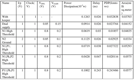
Table 1. Optimum Values for 2 input OR gate Name I/p (V) Clock( V) VDDL (V) VGndH (V) Power
Dissipation(10-5w)
Delay (ns) PDP(femto ws) Area(mi lli sq.meter ) With keeper
1 1 - - 0.1263 0.026 0.032838 0.03703
Dual supply
1 1 0.85 0.15 0.0914 0.026 0.023764 0.04152
N1 High Threshold
1 1 0.8 0.2 0.0619 0.03 0.01857 0.04835
N2 Ground
2 1 0.85 0.1 0.1125 0.026 0.02925 0.0334
N1,P1, High Threshold
1 1 0.8 0.2 0.0719 0.038 0.027322 0.05293
N1,Pk,P2 High Threshold
1 1 0.8 0.2 0.0428 0.047 0.020116 0.0575
P11,Pk,P1 High Threshold
1 1 0.8 0.2 0.1002 0.243 0.243486 0.0577
Table 2. Optimum Values for 16 input OR gate
Name I/P (V) Clock (V) VDDL (V) VgndH (V) Power Dissipation (10-5w)
Delay (ns)
PDP(10-15 w-s)
Area(milli sq.meter)
With keeper
1 1 - - 0.1834 0.078
0.143052
0.17056 Dual
supply
1 1 0.85 0.15 0.1634 0.078
0.127452
0.18618 N1 High
Threshold
1 1 0.8 0.2 0.1189 0.083
0.098687
0.19553 N2
Ground
1 1 0.8 0.1 0.2163 0.078
0.168714
0.18134 N1,P1,
High Threshold
1 1 0.8 0.2 0.1255 0.091
0.114205
0.20092
N1,Pk,P2 HighThres hold
1 1 0.8 0.2 0.0931 0.133
0.123823
0.2094
P11,Pk,P1 HighThres hold
1 1 0.8 0.2 0.0268 0.503
0.134804
Table 3. Optimum Values for 2 input AND gate
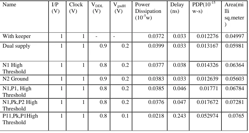
Table 4. Optimum Values for 2 input EX-OR gate
Name I/P
(V) Clock (V) VDDL (V) VgndH (V) Power Dissipation (10-5w)
Delay (ns) PDP(10-15 w-s) Area(mi lli sq.meter )
With keeper 1 1 - - 0.0372 0.033 0.012276 0.04997
Dual supply 1 1 0.9 0.2 0.0399 0.033 0.013167 0.05981
N1 High Threshold
1 1 0.8 0.2 0.0377 0.038 0.014326 0.06364
N2 Ground 1 1 0.9 0.2 0.0383 0.033 0.012639 0.05603
N1,P1, High Threshold
1 1 0.8 0.2 0.0385 0.046 0.01771 0.06784
N1,Pk,P2 High Threshold
1 1 0.8 0.2 0.0376 0.047 0.017672 0.07281
P11,Pk,P1High Threshold
1 1 0.8 0.1 0.0218 0.243 0.052974 0.0765
V.Conclusions
In the deep submicron of a technology, power delay product must be reduced to increase the efficiency of a circuit. The circuit techniques employing dual thresholds, dual voltages, dual grounds are presented in this work for simultaneously reducing power dissipation and delay in domino circuits and also to increase the noise immunity. The parameters of power dissipation, delay and power delay product are calculated for 2-input AND, OR, XOR and 16-input OR using different techniques in 65nm technology. From the results it can be concluded that the proposed logic technique which is dual threshold, dual ground and dual supply voltage with N1 high threshold shows good performance when compared to single threshold domino logic techniques. Hence it can be concluded that CMOS
Name I/P (V) Clock (V) VDD L (V) Vgnd H (V) Power Dissipation (10-5w) Delay(ns) PDP (10-15 w-s) Area(milli sq.meter)
With keeper 2 1 - - 0.0775 0.029
0.022475 0.03099 Dual supply 2 1 0.85 0.15 0.0857 0.028
0.023996 0.03699 N1 Threshold 2 1 0.8 0.2 0.0618 0.033
0.020394 0.0417
N2 Ground 2 1 0.85 0.2 0.104 0.032
0.03328 0.03516 N1,P1,
HighThreshol d
2 1 0.8 0.2 0.0607 0.036
0.021852
0.04322
N1,Pk,P2 High Threshold
2 1 0.8 0.2 0.0409 0.111
0.045399
0.05056
P11,Pk,P1Hi gh Threshold
2 1 0.8 0.1 0.0163 0.215
0.035045
logic techniques proposed in this work yield low power, high performance operation with increased noise immunity. Hence, it is concluded that the proposed designs will provide a platform for designing high performance and low power digital circuits such as processors and multipliers.
Acknowledgement
The authors wish to thank RGMCET, Nandyal, A.P, India for providing the Microwind3 and DSCH tools
References
[1] S. Borkar, “Obeying moore’s law beyond 0.18 micron,” in Proc. IEEE Int. ASIC/SOC Conf., Sept. 2000, pp. 26–31. [2] R. Ronen et al., “Coming challenges in microarchitecture and architecture,”Proc. IEEE, vol. 89, pp. 325–339, Mar. 2001.
[3] M. T. Bohr, “Nanotechnology goals and Challenges for electronic applications, ”IEEE Trans.Nanotechnoly, vol. 1, pp. 56–62, Mar. 2002. [4] D. J. Frank et al., “Device scaling limits of Si MOSFET’s and their application dependencies,” Proc. IEEE, vol. 89, pp. 259–288, Mar.
2001.
[5] R. K. Krishnamurty, A. Alvandpour, V. De, and S. Borkar, “High-performance and low-power challenges for sub-70 nm microprocessor circuits,”in Proc. IEEE Custom Integrated Circuits Conf., May 2002, pp.125–128.
[6] S. Mutoh et al., “1-V power supply high-speed Digital circuit technology with multithreshold- voltage CMOS,” IEEE J. Solid-State Circuits, vol.30, pp. 847–854, Aug. 1995.
[7] V. Kursun and E. G. Friedman, “Domino logic with dynamic body Biased keeper,” in Proc. Eur. Solid- State Circuits Conf., Sept. 2002, pp.675–678.
[8] “Variable threshold voltage keeper for contention reduction in dynamic circuits,” in Proc. IEEE Int. ASIC/SOC Conf., Sept. 2002, pp.314– 318.
[9] S. Borkar, Low Power Design Challenges for the Decade, Proceedings of the IEEE/ACM Design Automation Conference, pp. 293-296, June 2001.
[10] P. Srivastava, A. Pua, and L. Welch, .Issues in the Design of Domino Logic Circuits, Proceedings of the IEEE Great Lakes Symposium on VLSI, pp. 108-112, February 1998.
[11] G. Balamurugan and N. R. Shanbhag, .Energy- efficient Dynamic Circuit Design in the Presence of Crosstalk Noise,. Proceedings of the IEEE International Symposium on Low Power Electronics and Design, pp. 24-29, August 1999.
[12] Salendra.Govindarajulu, Dr.T.Jayachandra Prasad “Considerations of Performance Factors in CMOS Designs,” in Proc. of 2008 International Conference in Electronic Design, IEEE , December 1-3, 2008, Penang, Malaysia.
[13] Salendra.Govindarajulu, Dr.T.Jayachandra Prasad “Low Power, Energy-efficient Domino logicCircuits,”CEE2009, IJRTE, Volume 2, Number 7, November 2009,pp.30-33.
Biographical Notes
1
Salendra.Govindarajulu:- He is working as an Associate Professor in the Dept. of Electronics & Communication Engg. at RGMCET, Nandyal, Andhra Pradesh, India. He presented more than 11 International/National Technical Papers. He is a Life Member of ISTE, New Delhi. His interest includes Low Power VLSI CMOS design.
2