Space Vector PWM Signal Generation for a
Three Phase Inverter and Hardware
Implementation Using µ- Controller
B. Muralidhara1
Department of Electrical and Electronics Engineering, BMSIT, Yelahanka, Bangalore,Visvesvaraya Technological University, Belgaum, India, E- mail: [email protected].
A. Ramachandran2
Department of Electronics and communication Engineering, Vemana Institute of Technology, Koramangala, Bangalore,Visvesvaraya Technological University, Belgaum, India, E- mail: [email protected].
A. Srinivasan2
Department of Electronics and communication Engineering, Vemana Institute of Technology, Koramangala, Bangalore,Visvesvaraya Technological University, Belgaum, India
M. Channa Reddy2
Department of Electronics and communication Engineering, Vemana Institute of Technology, Koramangala, Bangalore,Visvesvaraya Technological University, Belgaum, India
Abstract:— This paper presents the space vector definitions for the flux, current and the voltage in a three phase system. In this paper, a Space Vector PWM signal generation for a conventional 3-phase inverter by comparing the reference phase voltages with the reference voltage vector is presented. The sector in which the tip of the reference vector lies is found out and the proposed Space Vector-PWM (SVPWM) method generates the inverter leg switching times, from the sampled reference phase voltage amplitudes in a sampling interval. Here Vdc is the
conventional three phase inverter DC link voltage. To generate gating signals PIC µ- controller is used in addition to the interface circuit. The present work explains the gating signal generation and implementation by SVPWM using µ- controller.
Key Words: Sine-Triangle PWM, Space Vector PWM, Multilevel inverter, PIC µ- controller.
I. Introduction
Pulse width modulated voltage source inverter fed drives are preferred in industries for variable speed applications [1,2,3]. . Among the various pulse width modulation (PWM) schemes, sine- triangle comparison method is the
description and implementation scheme for the space vector based PWM technique using reference phase voltages are explained. A space vector can be considered as a rotating vector [4.8]. A three phase stator winding (Fig.1.) of an induction motor when excited by a balanced 3-phase supply (sinusoidally varying) produces a rotating magnetic field [5-12] in the air gap. Such a field can also be generated by two coils orthogonally oriented.( Fig.2 ).In 3-phase system having currents isa(t), isb(t) and isc(t), the current space vector is
i
s(t)=i
sa(t)+i
sb(t)e
j2П/3+i
sc(t)e
j4П/3.Interms of two-phase components of the original 3-phase currents along the 2-phase axes, the current space vector is is(t) = is(t) +jis(t) In a similar way a space vector definition for the voltages, associated with the three phase system can also be expressed.
Fig.1. Three phase stator winding-schematic representation. Fig.2. Equivalent two phase representation of a 3- phase system
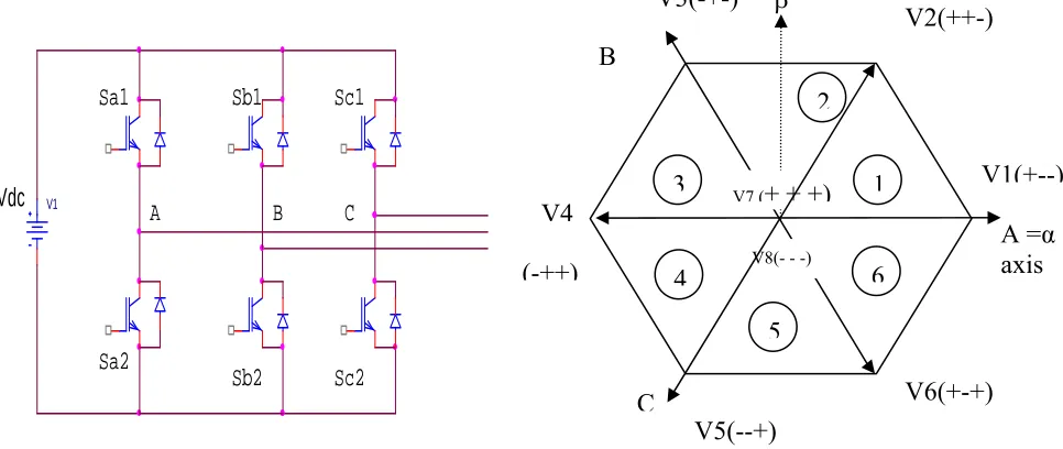
II. Three Phase PWM Voltage Generation from Voltage Space Vectors
Power stage of the three phase inverter is shown in Fig.3. A rotating voltage space vector of constant amplitude along a circular trajectory can be approximated between appropriate vectors in a sector (Fig.4.)[8]. A sampled reference vector Vs(t) is shown in Fig.5.
Fig. 3. Power Stage of three Phase Inverter Fig. 4. Space vector diagram of the effective vectors.
Let V1 be the starting vector of the sector-1 and V2 be the end vector of the sector-1[12]. The rotating reference
vector
V
s
is sampled at a constant frequency and during a sampling interval let theV
s
vector in a sector be making an angle ‘’ with the reference axis(V1starting vector of a sector).The stationary vectorV
s
during the samplingSb2
B
Sc1
Sa1
C
A
Sa2
Sc2
V1Vdc
Sb1
A
C
i
sc(t)
i
sa(t)
i
sb(t)
Ns
Ns
Ns
N
B
Ns
Ns
is
(t)
is
(t)
A =
α
axis
V5(--+)
V3(-+-)
(-++)
V4
V1(+--)
C
V2(++-)
5
3
2
1
6
4
V6(+-+)
B
V7 (
+ + +)
interval Ts can be generated by switching between V1 and V2 (end vector of a sector) and the zero vector (V7 or V8)
for a period T1, T2 and T0, such that the volt-seconds produced by the V1 and V2 vector states along the axis and
-axis will be equal to that of the
V
s
vector along axis and β-axis. There are eight switching states of the three phase inverter[5,7,8]V1 (+--) to V8 (---) as shown in Fig.4. Out of these eight switching states all plus V7 (+++) andall minusV8 (---) states are called zero state. One such switching state of a 3- phase inverter is shown in Fig.6.
Fig. 5.Sampled reference vector in sector-1 Fig. 6. Sample Switching state of a three phase inverter.
Fig.8. Black Diagram representation of gating signal generation.
Fig.7. Actual gating signal pattern in sector-1.
III. Voltage Space Vectors -Six Step Inverter.
All(+++) implies all the top switches are ON and (---) implies all the bottom switches are ON. The inverter switching vectors distribution during the switching periods T1, T2 and T0 in sector1 (V1, V2, V7 andV8) is as shown
in Fig.7 In the space vector based PWM method, the zero sequence voltage vectors V7 and V8 is distributed
symmetrically in one sampling period to reduce current ripple. In case of sector-1, the switching sequence is given
s
V
(t)
α
-axis
V1
α
060
0V2
β
-axis
B A VdcV1(+ - -)
C
Sb2
TCLOSE = 0
1
2
Sa1
TCLOSE = 0
1
2
Sc2
TCLOSE = 0
1
2
Sc1
TOPEN = 0
1
2
Sa2
TOPEN = 0
1
2
Sb1
TOPEN = 0
1
2
INVERTER SWITCHING PERIOD
V8 V1 V2 V7 V7 V2 V1 V8 T0/2 T1 T2 T0/2 T0/2 T2 TI T0/2
Ts Ts
by V8, V1, V2, V7, V7, V2, V1 and V8 within two sampling periods. The right aligned sequence is the simple way to
synthesize the output voltage vector is to turn ON all the bottom (or top) switches at the beginning of the switching cycle and then to turn them OFF sequentially so that the zero vector is split between V7 and V8 equally.
IV. Hardware Implementation
This section presents the hardware implementation in the laboratory. There are several steps involved in implementing the hard ware which can be represented in the block diagram shown in Fig.8. Here 5 V DC supply is given to PIC µ- controller and the Timer circuit , the output of the µ- controller is fed to interfacing circuit, than to the opto isolator circuit , which isolates the high voltage of the inverter circuit (400V dc) from the rest of low voltage TTL and other low voltage components. The output of the opto isolator and the interface circuit is fed to the gate of each switching device. Each opto isolator is excited by independent power supply for isolation purpose. The microcontroller needs to supply signals to a controller which controls an inductive load such as a motor. Back EMF spikes from an inductive load can easily glitch, or destroy a microcontroller. Back EMF spikes typically manifest themselves as very short duration spikes which may or may not contain enough energy to actually destroy a microcontroller. Hence by using the opto coupler such high voltage spikes etc can be prevented.
V. Results
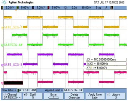
The oscilloscope recordings (Figures 9 and 10) shows three gating signal output from the microcontroller high frequency signal is added and the same has been fed to the gates of the corresponding devices. All the gating signals of the corresponding legs are shown in Figures(11- 14) . The typical inverter output voltages of Phase voltage, Line voltage, Sum of phase currents and Star point of Stator to general ground with induction motor as load are shown in fig.15 and 16.
FIG. 9. µ- controller output(10ms/Div). Ch.1. Gating signal for the leg A top switch
Ch.2. Inversion of Gating signal for leg A bottom switch.Ch.3. Gating signal for the leg B,top switch. Ch.4.Inversion of Gating signal for the leg B, bottom switch
FIG.10. µ- controller output(10ms/div). Ch.1. Gating signal for the leg B top switch
FIG.11. Opto Isolator Input(10ms/Div).
Ch.1. Gating signal for the leg B top switch Ch.2. Inversion of Gating signal for leg B bottom switch.Ch.3. Gating signal for the leg C top switch. Ch.4.Inversion of Gating signal for the leg C, bottom switch.
FIG.12. Opto Isolator Input(10ms/Div).
Ch.1. Gating signal for the leg B top switch . Ch.2. Inversion of Gating signal for leg B bottom switch. Ch.3. Gating signal for the leg A top switch. Ch.4.Inversion of Gating signal for the leg A, bottom switch.
FIG.13. Opto Isolator output (10ms/Div). Ch.1. Gating signal for the leg B top switch
Ch.2. Inversion of Gating signal for leg B bottom switch. Ch.3. Gating signal for the leg A top switch. Ch.4.Inversion of gating signal for the leg A, bottom switch.
FIG.14. Opto Isolator Output(10ms/Div). Ch.1. Gating signal for the leg B top switch
VI. Conclusion
The space vector modulation pulses have been generated using the PIC μ-Controller. Here the pulses are generated to get 40Hz a.c supply output from the inverter bridge. The signal generated has been suitably added with high frequency pulses, after Opto - isolation the same has been monitored and the wave forms are shown in the figs. 13 and 14 . For the experimental verification of the pulses, the same has been checked with the inverter bridge and it gives the satisfactory results which are shown in the fig. 15 and 16. The same methodology can also be used for the closed loop system with some modifications and the same has not been dealt here Hence it is concluded that the SVPWM pulses can be generated using the μ-Controller for the 3-phase inverter (Two- Level) circuits.
References
[1] J. Holtz, “ Pulse width modulation – A Survey”, IEEE Transactions on Industrial Electronics, Vol. 30, No.5, Dec 1992, pp. 410-420
[2] Keliang Zhou, and Danwei Wang, “Relationship between space vector modulation and three phase carrier- based PWM: A
Comprehensive Analysys”, IEEE Transactions on Industrial Electronics, vol. 49, No.1, February 2002, pp. 186-196.
[3] G. Narayanan, and V.T. Ranganathan, “Synchronised PWM strategies based on space vector approach I: Principles of waveform
generation”, IEE Proceedings- Electric Power Applications, vol 146, No.3, May1999, pp. 267-275
[4] N. Mohan, T.M. Underland, and W.P. Robbins, J. D. Irwin, “Power Electronics: Converters, Applications and Design”, John Wiley &
Sons Inc., 2nd ed., 1995.
[5] B. K. Bose, “Power Electronics and Veriable Friquency Drives: Technology and Applications”, IEEE Press and John Wiley &sons,
Inc.
[6] R. Krishan, “Electric Motor Drives: Modeling, Analysis and Control”, Printice Hall, 1999.
[7] W. Leonhard, “Control of Electrical Drives”, Springer Verlag, 2001.
[8] D.G. Holmes, T. A. Lipo, “Pulse Width Modulation for Power Converters: Principles and Practice” IEEE Press series on Power
Engineering.
[9]. H. J. Kim, H.D. Lee, and S. K. Sul, “A new PWM strategy for common mode voltage reduction in neutral point clamped inverter fed
AC motor drives”, IEEE Transactions on Industry Applications, Vol.37, No. 6. Nov/Dec. 2001, pp.1840-1845
[10]. Chapter 2. 16F877 PIC micro controller- Over View, Data sheets,
[11]. Dubay, G.K. “Power semiconductor controlled drives”, pp 283-342, 1989, Printice- Hall, Inc
FIG.15. Input to Motor (20ms/Div).
Ch 1: 200: 1 Phase voltage to Induction Motor Ch 2: 200: 1 Phase voltage to Induction Motor Ch 3: 200: 1 Phase voltage to Induction Motor Ch 4: 200: 1 Star point to ground
FIG.16. Input to Motor (20ms/Div).
Ch 1: 200: 1 Phase voltage to induction motor Ch 2: 200: 1 Line voltage to Induction Motor Ch 3: 20: 1 Sum of phase currents