IJSRST1845426 | Received : 05 April 2018 | Accepted : 20 April 2018 | March-April-2018 [ (4) 7 : 222-226]
© 2018 IJSRST | Volume 4 | Issue 7 | Print ISSN: 2395-6011 | Online ISSN: 2395-602X Themed Section: Science and Technology
222
Design and Benchmarking of Gigabit Transceiver Protocol for
45nm based FPGA
Aniket J. Prajapati*1, Himanshu Tyagi2, Naresh Kumar Gardas3
1Electronics & Communication, GTU PG School, Gandhinagar, Gujarat, India
2Negative Ion Lab, Institute For Plasma Research (IPR), Gandhinagar, Gujarat, India
3Cource Coordinator, Centre For Development of Advanced Computing (C-DAC), Pune, Maharashtra, India
ABSTRACT
This paper gives the design of link where the parallel digital data are transmitted serially at the rate of 2.5Gbps on the Spartan 6 evaluation board. The implemented design is to test Gigabit Transceiver Protocol in order to transfer 16-bit parallel data serially over the SMA cable in full duplex mode. The 16-bit Parallel data are transmitted and received by the Serialized/De-serialized (SERDES) using Multi-Giga bit transceiver (MGT) at the clock rate of 125MHz.Gigabit Transceiver Protocol converts the parallel data to serial and serial to parallel. The proposed design is simulated in Xilinx 14.7 and implemented on Spartan 6 FPGA. The serial data are transmitted at the rate of 2.5Gbps over the SMA Cable link.
Keywords: Gigabit Transceiver Protocol, Multi-Giga bit transceiver (MGT), Phase-locked Loop (PLL), ChipScope Pro Analyzer.
I.
INTRODUCTION
The field signal from any test facility gives the 16-bit parallel digital signals. The digital data are transmitted serially through SMA Cable and converted serial to parallel at the end of the receiver side. So, Number of the SMA Cable link can be reduced to transfer each field signals by using wave division multiplexing and reconstructed 16-bit parallel digital signals at the receiver side.
The paper gives the solution to encode the parallel data into the serial form and also gives the solution for the PLL based clock and data recovery at the end of receiver side with the use of 8b/10b encoder.
A Multi-Giga bit transceiver (MGT) is an SERDES capable of operating at serial bit rates above 1 Gigabit/second. MGTs are used increasingly for data communications because they can run over longer
distances, use fewer wires, and thus have lower costs than parallel interfaces with equivalent data throughput.
Chapter I. Introduction about the Paper, Chapter II. GTP Architecture, Chapter III. Simulation and Testing using ChipScope Pro, Chapter IV. Conclusion, and Chapter V. References.
II.
GTP ARCHITECTURE
The GTP transceiver is a power-efficient transceiver for Spartan®-6 FPGAs. The GTP transceiver is tightly integrated and highly configurable with the programmable logic resources of the FPGA. It provides the following features to support a wide variety of applications:
Current Mode Logic (CML) serial drivers/buffers
Programmable TX pre-emphasis, linear
continuous-time RX equalization
Optional built-in PCS features, such as 8B/10B
encoding, comma alignment, channel bonding, and clock correction
Support for multiple industry standards with the
following line rates:
i. 0.614 Gb/s to 0.810 Gb/s ii. 1.22 Gb/s to 1.62 Gb/s iii. 2.45 Gb/ to 3.125 Gb/s
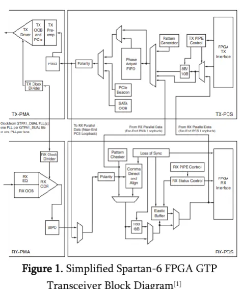
Their shown in Figure 1 is Simplified Spartan-6 FPGA GTP Transceiver Block Diagram. Here inside the block diagram PCS (physical coding sublayer) and PMA (physical medium attachment). Their PMA main Work Serial Data Transmit (Tx) and Parallel Data Receive (Rx), inside the PMA SIPO, Clock Divider, PISO and etc. As well PCS inside FIFO, PCIe, PRBS Generator, Frame Checker, 8B/10B, FPGA and etc.
Figure 1. Simplified Spartan-6 FPGA GTP Transceiver Block Diagram[1]
GIGABIT TRANSCEIVER PROTOCOL
This LogiCORE IP GTP is lightweight, scalable, link layer protocol for high-speed serial communication. This protocol is very useful for low-cost, high-rate
can be implemented through the Xilinx environment. The user application interface of the protocol can be seen in figure
As per the specification, the protocol contains one more lanes. Each lane is full duplex serial data connection. That can transmit the serial data at the rate from 0.6 Gb/s to 2.5 Gb/s. With the help of channel partner, the user device can communicate together. Those channels are automatically initiated a channel when they are connected to a channel partner. After the initialization, the user application can transfer the data across the channel as a stream of the framing data structure.The GTP provides two type of transmission mode:
1. Full Duplex mode,
2. Simplex Mode (Tx- only simplex and Rx- only simplex)
The transmission mode for this design is full duplex mode. The protocol can be customized as per the design.
Lane width decides the number of bytes transmitted during the period of one clock cycle. This GTP supports PCI Express and 4 lane width.
If the selected lane width is 4 then the user clock (USRCLK) should be half of reference clock (REFCLK). The multi-Giga bit transceiver is configured using GTP that converts each byte of data i.e. 2 byte of data into 20 bits (each byte i.e. 8 bits into 10 bits). Here GT REFCLk is 125 MHz, which is generated through PLL. So the Line rate will be 125 MHz * 20 (bits) equal to 2.5 Gb/s. At this data rate, the serial data are transmitted over the SMA channel.
MULTI-GIGA BIT TRANCEIVER
In serializer, the encoder will modify the parallel data & adds some overhead bit. It helps in synchronization and channel transmission in serial. Also, it used to achieving DC balancing, error detection, and clock recovery. In 8B/10B encoding scheme, 8-bit input data is serialized at 10x serial clock. PLL is used to generate serial clock (10x) from the parallel clock. And that serial data transmitted over the differential channel, where at receiver side Deserializer word synchronizer finds word packet boundaries from serial data. The main function of Deserializer is clock and data recovery (CDR). It receives serial data and extracts the synchronized clock either from data itself or generates the synchronized serial clock from reference parallel rate clock. For that phase lock loop is required for both options.
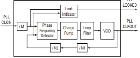
In PLL based clock and data recovery, a phase-frequency detector generates two output signals which are UP and DOWN signals and depends on the phase difference between the input data and the generated clock. A phase difference will be detected as a phase difference and the PDF will generate steady UP-DOWN signal. Now this signals cause the charge pump (CP) to output or source a current, which is converted into the voltage and filtered by the loop filter. This voltage controls the output frequency of VCO. This voltage controlled oscillator output is recovered clock; it will feed back to the phase frequency detector. This PLL’s negative feedback faces phase & frequency of the recovered clock to be same as the phase, bit rate, and clock condition. This PLL is Shown in Figure 2.
Figure 2. PLL Detail (Phase-lock Loop)[1]
GTP transceiver is a power efficient transmitter-receiver for Spartan 6 FPGA. In the physical implementation of MGTs; it takes the form of differential based electrical interface. There are three differential methods such as:
1. Current Mode logic (CML),
2. Low voltage differential signaling (LVDS) & 3. Low voltage Pseudo emitter coupled logic (LVPECL).
CML is most common and preferable for the Giga-bit link for AC or DC termination and selectable output drive. GTP provides programmable Tx_pre emphasis, linear continuous time Rx equalization. The GTP transceiver has the line rate of 3.125 Gb/s, which is implemented tested for the SMA link of 2.5 Gb/s line rate.
GTP MODULE INTERFACE
The Gigabit Transceiver Protocol (GTP) is compact and hot-pluggable transceiver used for both telecommunication also for data communication.
A. Software and Hardware Resources: 1. Xilinx ISE 14.7 tool.
2. Xilinx Core Generator.
3. Xilinx LogiCORE IP GTP Tranceiver wizard core.
4. Xilinx Spartan 6 (SP605) hardware development board.
5. SMA cable.
6. GTP transceivers in ChipScope Pro Analyzer.
III.
SIMULATION AND TESTING USING
CHIPSCOPE PRO
Figure 4: GTP Transmit Data at 1860.10200 ns
Figure 5. GTP Receive Data at 2036.15400 ns
Here, Difference between receive and transmit data through find a latency. In GTP Transmit Data and Receive Data difference latency equal to 176.052ns.
Figure 6. Listing table of GTP Transmit and Receive Data
The testing results give the transmitted and received bit pattern on the input data. The transmitted input sequence can be seen at the end of the listing table in chipscope pro analyzer tool [6] (Figure 6). Figure 7 shows waveform of the GTP_TX_DATA sequence and
Figure 7. Waveform of GTP Transmit and Receive Data
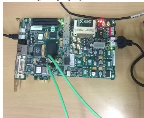
Figure 8 shows the Hardware implementation as shown them. To Spartan-6 FPGA Board (sp605) is 45nm technology using High-speed Data transfer.
Figure 8. Implementation GTP Transceiver on Board
IV.
CONCLUSION
V.
ACKNOWLEDGMENT
The authors would like to thank Negative ion Beam Department at the Institute for Plasma Research Center, Bhat - Gandhinagar to support in design and implementation of hardware.
VI.
REFERENCES
[1] Xilinx.com. (2018). [online] Available at: https://www.xilinx.com/support/documentation/u ser_guides/ug386.pdf [Accessed 11 Apr. 2018]. [2] Xilinx.com. (2018). [online] Available at:
https://www.xilinx.com/support/documentation/i p_documentation/s6_gtpwizard_gsg546.pdf [Accessed 12 Apr. 2018].
[3] Xilinx.com. (2018). [online] Available at: https://www.xilinx.com/support/documentation/i p_documentation/s6_gtpwizard/v1_10/ug546_s6_g tpwizard.pdf [Accessed 12 Apr. 2018].
[4] Xilinx.com. (2018). [online] Available at: https://www.xilinx.com/support/documentation/s w_manuals/xilinx11/chipscope_pro_sw_cores_ug0 29.pdf [Accessed 13 Apr. 2018].
[5] Xilinx.com. (2018). [online] Available at: https://www.xilinx.com/support/documentation/s w_manuals/xilinx14_6/ug750.pdf [Accessed 15 Apr. 2018].
[6] Xilinx.com. (2018). [online] Available at: https://www.xilinx.com/support/documentation/b oards_and_kits/ug526.pdf [Accessed 16 Apr. 2018].