70 |
P a g e
DESIGN AND ANALYSIS OF I
2
C BASED DATA
TRANSMITTER AND RECEIVER
M. Arul Kumar
1, P. Priyadarshini
2, M. Saravanan
3 1,2PG students / VLSI Design, SNS College of Technology, Coimbatore, (India)
3
Assistant professor / ECE Department, SNS College of Technology, Coimbatore,(India)
ABSTRACT
As technology scales, the physical size of the Integrated Circuit(IC) is reduced by means of reducing the transistor
count and Input Output (I/O) pins. In order to minimize the I/O pins the interconnect delays will be reduced
internally. In major applications the integrated circuits plays a major role because it control faster devices to
communicate with slower devices and also allow devices to communicate with each other over a serial data bus
without data loss. Hence to allow serial communication and to reduce the interconnect delays the I2C
(Inter-Integrated Circuit) protocol is considered. The I2C controller provides support for a communication link between
integrated circuits and memory units on a board.I2C is a two wire, bidirectional serial bus that provides effective
data communication between two devices. I2C bus supports many devices and each device is recognized by its
unique address. Secure Digital is the most widely used portable memory standard. Its ultra-compact and rugged
architecture, simple interface, high security, low power consumption and reliable operation. This module was
designed in Verilog HDL and synthesized using Xilinx ISE Design Suite 13.2.
Keywords: Inter-Integrated Circuit, Finite State Machine, Serial Data, Serial Clock, FPGA, Verilog.
I.
INTRODUCTION
The physical size and power requirement of IC get reduce over the years. The main reason for that is more number
of transistors can be integrated into smaller size and less number of interconnections wire present in between ICs
can possible. The actual circuitry of the IC is much smaller than the packaging of the IC but it requires larger area to
cover because of interconnection wire present in between ICs. These wire requirements can be reduce by using I2C
that is Inter-Integrated circuit bus. This communication has a special protocol assigned to it which is I2C Protocol.
I2C bus physically consists of two active wires and a ground connection. The two active wires namely Serial
Clock(SCL) and Serial Data (SDA). These wires are bidirectional half duplex in natures which carry information
between the devices connected to the bus. Each device is acknowledge by a unique address whether it is a
microcontroller, LCD driver, memory or keyboard interface and can operate as either a transmitter or receiver,
depending on the function of the device. In I2C bus devices can easily added or removed which is very useful for
71 |
P a g e
design much more important application includes serial communication like sensors communication with personal
computer. Many common embedded system peripherals, such as analog-to-digital and digital-to-analog convertors,
LCDs, and temperature sensors, support serial interfaces. The objective of this project is to design and analyse the
data transmitter and receiver by using an I2C bus protocol by using Verilog hardware description language and
synthesis by the software Xilinx.
II.
NEED FOR I
2C BUS
The on-chip RAM (EEPROM), Oscillator (RTC), ADC and I2C Interface will be integrated for the purpose to
Communicate between them. The presence of a RTC and an on-chip RAM introduces an immediate need for a data
communication between the chip and a host computer to send data on the RAM. To minimize the system-level
interconnect, the contents of the RAM storing the results back to a host computer via a serial bus, the I2C Interface.
This greatly simplifies the system level design and in particular the design of the mother-board and associated
chip-boards. Moreover, storing data in a digital format on-chip before transmittal to a host computer over the I2C
Interface will result in an improved system performance since the transmission of digital data is much less
susceptible to interference from environmental noise sources.
2.1.
Design goals
The following goals were considered during this design:
I 2C bus speeds of 100kbits/sec and 400kbits/sec
I 2C 7-bit addressing
Multiple I 2C masters on one I2C bus
Up to 256-byte I 2C transactions
Compatible with any number of slaves
2.2.
I
2C features
Only two bus lines are required: a serial data line (SDA) and a serial clock line (SCL).
Each device connected to the bus is software addressable by a unique address and simple
master/slave relationships exist at all times masters can operate as transmitters or as
master-receivers.
It‟s a true multi-master bus including collision detection and arbitration to prevent data corruption if
two or more masters simultaneously initiate data transfer.
Serial, 8-bit oriented, bi-directional data transfers can be made at up to 100 bit/s in the
Standard-mode, up to 400 kbps in the Fast-Standard-mode, or up to 3.4Mbps in the High-speed mode
III.
I
2C BUS PROTOCOL
The interconnect integrated circuit bus commonly known as the I2C bus which is a bi-directional, two-wire and
serial communication standard protocol. It is designed primarily for simple but efficient integrated circuit (IC)
72 |
P a g e
Fig. 1 I
2C Bus Configuration
The system is comprised of two bus lines, SCL (Serial Clock) and SDA (Serial Data) that carry information between
the ICs connected to them. Various communication configurations may be designed using this bus however this
application discusses only the Master-Slave system implementation.
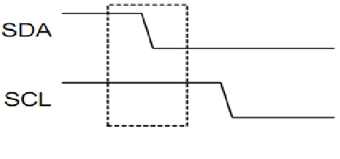
3.1. START CONDITION
The master initiates a data transfer by issuing a START condition, which is a high to low transition on the SDA line
while the SCL line is high as shown in Figure 2. The bus is considered to be busy after the START condition. After
the START condition, a slave address is sent out on the bus by the master. This address is 7 bits long followed by an
eight bit which is a data direction bit (R/~W) where a „0‟ indicates a write from the master to the slave and a „1‟
indicates a read from the slave to the master.
Fig. 2 START Condition
The master is controlling the SCL line, will send out the bits on the SDA line, one bit per clock cycle of the SCL
line ,with the most significant bit sent out first. The value on the SDA line can be changed only when the SCL line is
at low.
3.2. STOP CONDITION
The START condition happens when the SDA line changes from a high to a low while the SCL line is at a high. The
STOP condition happens when the SDA line changes from a low to a high while the SCL line is high. These are the
73 |
P a g e
Fig. 3 START Condition
IV.
I
2C PROPOSED
4.1.
Master Implementation
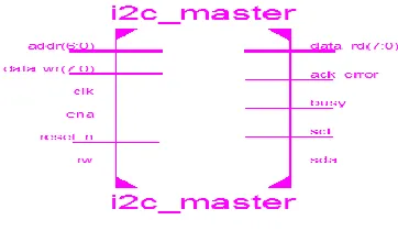
I2C Master is composed of a Slave and some additional components. The I2C Master is connected to a controller
from which it receives destination address, control signals and data. A Master must have the ability to create the I2C
Serial Clock, START and STOP signals. It also has to keep track of the number of transferred bytes to determine an
appropriate time to stop a data transfer. Based on the above characteristics a shortcut was used to take advantage of
the already created Slave. There are two types of devices on the I2C bus, Master and Slave.
A Slave cannot initiate a data transfer. It just monitors the SDA and SCL lines waiting for a START signal. After
detecting a START signal, the Slave will compare its address to the address received. If the addresses match, it will
perform an action requested by Master by either sending or receiving data.
Fig. 4 Master Logic
4.1.1. Finite State Machine
The Finite State Machine (FSM) is the most important component in the design of the Master to accommodate this
requirement; both Master and Slave Microcontroller are slightly changed from its original designs. In the
transferring mode (Master sends data to Slave), the FSM gets number of bytes from the Microcontroller before
releasing a Start condition. But in the receiving mode, the FSM gets the number of RAM locations in the first byte
received from Slave. After that it holds the SCL line low to freeze the communication, sending number of locations
back to controller. Controller will manipulate the number of locations to get number of bits and send it back to
Master.
4.1.2. Shift Register
The Shift Register is used for parallel-to-serial and serial-to-parallel conversion. It is an 8-bit Shift Register with
74 |
P a g e
edge of the SCL signal and shifts the received bit to the left. After getting the whole byte, the data will be parallel
loaded to the RAM. In the transmitting mode, the Shift Register is loaded with parallel data from the RAM first and
then the data will be shifted to the left to transfer each bit to a receiver on the negative edge of the SCL signal.
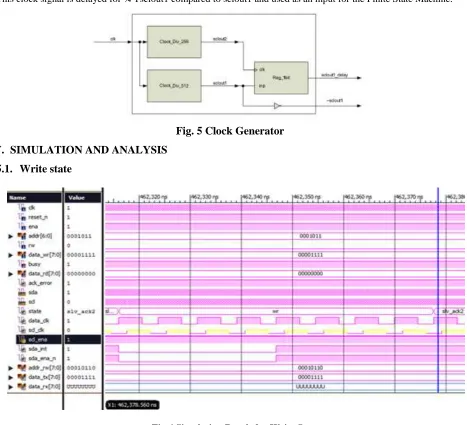
4.1.3 Clock Generator
The I2C Master will be downloaded to a Spartan 3E board, which operates at a frequency of 50MHz. In order to
create an approximately 100 KHz SCL signal, we need to divide the board clock signal by 512 times, the I2C Master
only changes the SDA signal when the SCL line is low, or equivalently, the Master can change SDA line signal at
negative edge of SCL signal. Hence, before negative edges of SCL, the circuit conditions, based on which the
Master makes its decisions, must be stable and valid. For this reason, the signal in addition to sclout1 called
sclout1_delay. This signal is used as the operating clock signal for the 32-bit counter inside the FSM. In order to
create this signal, in addition to the Clock_Div_512 module, we need a Clock_Div_256 module and a 1-bit register.
This clock signal is delayed for ¼ Tsclout1 compared to sclout1 and used as an input for the Finite State Machine.
Fig. 5 Clock Generator
V.
SIMULATION AND ANALYSIS
5.1.
Write state
75 |
P a g e
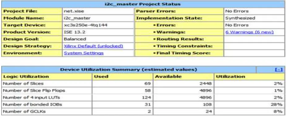
The above simulation output gives the detail picture of data can be write in to the memory address 00010110 and
after that slave responds as acknowledge that data is received.
Table 1 Logic utilization of proposed I
2C master unit
The design summary indicated in table 1 shows that the global clock used is 8%, the number of bounded input
output blocks utilization is 28%,hence the system interconnect will be minimized by reducing the flip flops.
VI. CONCLUSION
The design of I2C controller using Verilog HDL, simplifies the design process. The result shows successful storage
of data transmitted by the master and the power dissipation due to leakage is 0.052w analyzed by synthesis. The
result shows that minimal resources are utilized in designing the I2C master as only 2 % slices, 1% flip flops and 2%
LUTs are utilized. The logic synthesis tool will optimize the circuit in area and timing for the new technology. The
design of I2C master controller has immense applications in future as the number of devices connected to a system is
only going to increase. So there is always a need for a system which supports multiple protocols. The drawback of
designed I2C is that the bounded I/O utilization will be more when compared it with existing design. Dumping of
Verilog code to FPGA to realize the exact hardware of the circuit and the verification of I2C bus using system
Verilog based open verification methodology.
REFERENCES
[1] Bollam Eswari, N.Ponmagal, K.Preethi, S.G.Sreejeesh, “Implementation of I2C Master Bus Controller on
FPGA”, ICCSP/IEEE- Advanced technology,Pp-1113-1116, April 2013.
[2] Prof. Jai Karan Singh, “Design and Implementation of I2C master controller on FPGA using VHDL”,
76 |
P a g e
[3] F. Leens, “An Introduction to I2C and SPI Protocols,” IEEE Instrumentation & Measurement Magazine, pp.
8-13, February 2009
[4] A.K. Oudjida, M.L. Berrandjia, R. Tiar, A. Liacha, K. Tahraoui “FPGA Implementation of I2C & SPI Protocols
a Comparative Study” IEEE 2009
[5] A.R.M. Khan, A.P.Thakare, A.R.M. Khan, ”FPGA based design and implementation of serial data transmission
controller”, International Journal of Engineering Science and Technology Vol. 2(10), 2010, 5526-5533.
[6] The Fundamentals of Efficient Synthesizable Finite State Machine Clifford E. Cummings, Sunburst Design,
Inc. Xilinx, Inc. 2002
[7] I2C bus Inter Integrated Circuits bus by Philips Semiconductors.