e-ISSN: 2278-067X, p-ISSN: 2278-800X, www.ijerd.com
Volume 12, Issue 5 (May 2016), PP.15-22
Design, Implementation and Comparison of FFT Analysis of
efficient Digital PLLs for clock generation using 50nm SPICE
models for CMOS
Jayati Shukla, Paresh Rawat
Department of Electronics and Communication Engineering Truba College of Science and Technology Bhopal, India
Department of Electronics and Communication Engineering Truba College of Science and Technology Bhopal, India
Abstract:-
The most versatile application for digital phase locked loops is for clock generation and clock recovery in any complex computer architecture like a microprocessor or microcontroller, network processors. Digital Phase locked loops are commonly used to generate timing on chip clocks in high performance mixed signal analog and digital systems. Most of the systems employ digital PLL mainly for synchronization, skew and jitter optimization. Because of the need of high speed circuitry there is a need of PLL. Mostly communication, wireless systems, RF Processors operate in Gigahertz range, there is a necessity of PLL that too digital which operate in high order frequencies. Digital PLL is a mixed signal integrated circuit and presented work focuses on design and analysis of efficient digital phase locked loops for clock generation using 50nm SPICE models. The presented design Digital PLL performs the function of mainly generating a clock signal also consists of design of sub circuits and systems like phase detector, loop filters and voltage controlled oscillators. A detailed FFT analysis is also presented with parameters magnitude, phase and group delay calculated for each sub circuits and systems. The results of DPLL designed using proper optimization method is also compared with traditional method.Index Terms:-
Digital PLL, SPICE, VCO, Phase Detector, FFT, Loop filtersI.
I
NTRODUCTIONDigital Phase locked loop is a mixed signal analog integrated circuit. Digital PLL is the heart of many communication as well as electronic systems. Mostly a higher lock PLL range with lesser locking time and should have tolerable phase noise.
The most versatile application of a digital PLL is for clock generation or synchronization, clock recovery, communication systems and frequency synthesizers. In high performance digital systems like processors digital PLL or DPLL are commonly used to generate well timed on chip clock signals. Modern RF circuits or wireless mobile communication systems use PLL for synchronization, timing based synthesis, skew and jitter reduction. Digital PLL is extensively used in advanced communication systems, electronic and medical instrumentation systems. The PLLs are an integrated part of larger circuits on a single chip.
A simple PLL consists of namely four to five integrated blocks. They are phase frequency detector, charge pump, Loop filters, voltage controlled oscillator and frequency dividing circuits.
oscillating signal and generates an output waveform that exerts the same phase frequency relationship as the input signal. This is achieved by constantly comparing the phase of output signal to the input signal with a phase frequency detector (PFD).
The Phase frequency Detector (PFD) is one of the main parts in PLL circuits. It compares the phase and frequency difference between the reference clock and the feedback clock. Depending upon the phase and frequency deviation, it generates two output signals UP and DOWN. The Charge Pump (CP) circuit is used in the PLL to combine both the outputs of the PFD and give a single output. The output of the CP circuit is fed to a Low Pass Filter (LPF) to generate a DC control voltage. The phase and frequency of the Voltage Controlled Oscillator (VCO) output depends on the generated DC control voltage. If the PFD generates an up signal, the error voltage at the output of LPF increases which in turn increase the VCO output signal frequency. On the contrary, if a Down signal is generated, the VCO output signal frequency decreases. The output of the VCO is then fed back to the PFD in order to recalculate the phase difference, and then we can create closed loop frequency control system.
III.
PLL
A
RCHITECTUREIn general a PLL consists of five main blocks:
1. Phase Detector or Phase Frequency Detector (PD or PFD) 2. Charge Pump (CP)
3. Low Pass Filter (LPF)
4. Voltage Controlled Oscillator (VCO) 5. Divide by N Counter
Figure.2 A generic architecture of Digital PLL
3.1 Phase frequency Detector
Figure.3 Schematic Diagram for Phase frequency Detector
Figure.4 Icon view for schematic in Figure 3 PFD
Figure.5 Simulation plot for Up and Down signals in PFD
Figure.5 shows the waveform formed by the PFD. It has two waveform, one for UP signal and other for down signal.
3.2 Charge Pump and Loop Filter
Charge pump circuit is an important block of the whole PLL system.
Figure.7 Schematic for 21 stage Voltage Controlled Oscillator
3.4 Frequency Divider
The output of the VCO is fed back to the input of PFD through the frequency divider circuit. The frequency divider in the PLL circuit forms a closed loop. It scales down the frequency of the
VCO output signal. A simple flip flop (FF) acts as a frequency divider circuit. The schematic of a simple divider based divide by 2 frequency circuit is shown in the Figure 8
Figure.8 Schematic view for frequency divider network
IV.
D
ESIGN ANDS
YNTHESIS OFDPLL
Figure.9 Design of ADPLL from Base Paper [1]
Figure.10 DPLL using Op-amp, PFD and RC loop filter and Charge pump
Figure.9 is the design of ADPLL which were used in our Base Paper. But there are certain limitations in the design of ADPLL which is given in base paper, like, jitter problem, phase and timing, locking time, core area, performance, power consumption. So in this work, we are going to design our own ADPLL or DPLL with different components and try to remove all the problems of previous design.
Figure.10 is our own designed DPLL with different components. In this, as compare to Figure.9 we have used Phase/Frequency Detector (PFD) in place of BPD, Voltage Controlled Oscillator (VCO) in place of Digital Controlled Oscillator(DCO), divide by 2 divider in place of divide by N.
V.
S
IMULATIONR
ESULTSThis section describes the circuit, transient plot and waveform of different components obtained during the designing of DPLL.
Figure.12 Transient plot for VCO using simple inverter
Figure.13 FFT plot for VCO using simple inverter
Figure.14 Schematic for VCO using current starved CMOS Inverter
Figure.15 Transient plot for Vdata and Vclock in DPLL
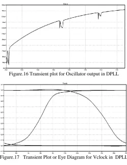
Figure.16 Transient plot for Oscillator output in DPLL
Figure.17 Transient Plot or Eye Diagram for Vclock in DPLL
VI.
FFT RESULTS
The following table summarizes the FFT analysis of designed DPLL with parameters like, frequency, magnitude, phase and group delay under different ranges.
Table 1 FFT analysis for designed DPLL Frequency Magnitude Phase Group Delay 1MHz -19.82 dB 109.74° 17.85 ns 10 MHz -37.42 dB 104.85° 48.016 ns 100 MHz -56.21 dB 92.41° -37.87 ns 1 GHz -78.79 dB 91.68° -3.414 ns 10 GHz -98.53 dB 105.14° -78.45ns 100 GHz -111.30 dB 179.99 ° -3.620 ns
VII.
CONCLUSION
In this paper presented DPLL works with better locking times, the digital PLL consumes low power as designed with 50 nm CMOS technology, the transient analysis mainly depends on the type of the PFD architecture used and parasitic parameters utilized for charge pumps and loop filters. So by properly choosing VCO architecture, PFD design and adjusting the charge pump configurations. The efficiency of the overall design also depends on the reduction of transistor sizes which is 50nm.
R
EFERENCES[1]. Dian Huang, Ying Qiao, “A fast locked all digital phase locked loop for dynamic frequency scaling”, Moon Seok Kim, Yong Bin Kim, Kyung Ki Kim, “All digital phase locked loop with local passive interpolation time to digital converter based on tristate inverter ” IEEE transactions 2012.
pp.665-[9]. Deok-Soo Kim, Heesoo Song, Taeho Kim, Suhwan Kim and Deog-Kyoon Jeong, “A 0.3-1.4 GHz All-Digital Fractional-N PLL with Adaptive Loop Gain Controller,” IEEE Journal of Solid-State Circuits, Vol.45, no.11, pp.2300-2311, Nov 2010.
[10]. Quan Sun, Yonguang Zhang, Christine Hu-Guo, Kimmo Jaaskelainen and Yann Hu, “A fully integrated CMOS voltage regulator for supply-noise-insensitive charge pump PLL design,” Microelectronics Journal, Vol. 41, Issue 4, April 2010, Pages 240-246
[11]. S.J.Li, and H.H.Hsieh,” A 10 GHz Phase-Locked Loop with a Compact Low-Pass Filter in 0.18 µm CMOS Technology”, IEEE Microwave and Wireless Components Letters, VOL. 19, NO. 10, OCTOBER 2009
[12]. H.Janardhan, and M.F.Wagdy “Design of a 1GHz Digital PLL Using 0.18 µm CMOS Technology,” IEEE Proc. of the Third International Conference on Information Technology,2006.
[13]. R.E. Best, “Phase Locked Loops Design, Simulation and Applications,” McGraw-Hill Publication, 5th Edition, 2003.
[14]. S.M.Kang, and Y.Leblebici, “CMOS Digital Integrated Circuits: Analysis and Design,” McGraw-Hill Publication, 3 rd Edition, 2003.
[15]. R.J.Baker, H.W.Li, and D.E.Boyce, “CMOS Circuit Design, Layout, and Simulation,” IEEE Press Series on Microelectronic Systems, 2002.
[16]. B. Razavi, “Design of Analog CMOS Integrated Circuits,” Tata McGraw Hill Edition,2002.
[17]. M.Mansuri, D.Liu, and C.K.Yang, “Fast Frequency Acquisition Phase Frequency Detector for GSamples/s Phase Locked Loops,” IEEE Journal of Solid State Circuit, Vol. 37, No. 10,Oct., 2002.
[18]. Youngshin Woo, Young Min Jang and Man Young Sung, “Phase-locked loop with dual phase frequency detectors for high-frequency operation and fast acquisition,” Microelectronics Journal, Vol. 33, Issue 3, March 2002, Pages 245-252.
[19]. S. M. Shahruz, “Novel phase-locked loops with enhanced locking capabilities,” Journal of Sound and Vibration, Vol. 241, Issue 3, 29 March 2001, Pages 513-523.