New Design And Prototyping Of Microcontroller
Based Physical Control Unit Utilizing Continuous
Control Algorithms.
Ahmad Alahmadi
Abstract : This paper presents the design and implementation of a microcontroller-based control unit utilizing continuous control algorithms. The parallel design approach is applied in the design and selection process. The suggested control unit design has number of features such as : (a) Arduino Due selected as microcontroller,(b) The unit is developed to run on 3.3VDC, (c) it allows to accept inputs of both the current and voltage type sensors’ signals i.e.; current (4 to 20 mA) and voltage (0 to 5 VDC and 0 to 3.3 VDC) respectively,(d) it generates four different types of control signal that include continuous signal type (0 to 5 VDC), PWM (0 to 255), current control (4 to 20 mA) and fully ON/OFF control signal type ,(e)The system supports both wired and wireless interfacing communication between the control unit, sensors and the actuator’s drive. (f)The system is designed with LCD for visual data displaying. The developed prototype was tested experimentally for LED light intensity control and the experimental results are presented.
Keywords: Control unit, Controller design, PID Control algorithm, Microcontroller.
————————————————————
1. INTRODUCTION
The advances in different scientific fields and the interdisciplinary synergistic integration of different engineering disciplines in the design and manufacturing of various new modern products, supported with the advances in manufacturing technologies, all this lead to developing new forms of existing products with modified capabilities. This work is focused on utilizing the modern scientific interdisciplinary advances, in the design of a new and flexible microcontroller-based control unit utilizing different control algorithms. In modern system design, two components are considered the most important that include the control unit (physical-controller) and the control algorithm (software). Different control devices are currently available that include Microcomputer, Microcontroller (μc), Personal computer (PC), Application-specific integrated circuits (ASICs), Digital signal processors (DSP), and Programmable logic controller (PLC). Apart from the control devices, different control algorithms have been reported in the existing literature, such as ON/OFF, proportional, integral and derivative (PID) control , adaptive control, Feed forward, intelligent (Neural network, Fuzzy logic, Genetic) and robust controllers. Each of these algorithms has its advantages and disadvantages. The control engineer must select the best control algorithm for given specific physical application. In this work the ON/OFF and PID control modes are implemented.
In the literature, different designs for microcontroller based control systems can be found, most of these designs are either concerned with developing new processor designs , or concerned with building customized control unit intended for specific applications, and depending on application, are designed to accept and output a particular type of control signals (i.e. voltage or current). Examples include; in [1] is presented the design of a General Purpose 8-bit RISC Processor for Computer Architecture Learning. In [2] control unit design of a 16-bit processor using VHDL is presented. In [3] Authors presented the design and implementation of special purpose control system for application, only, in elevator system control. In [4] Authors presents a special purpose a low cost and flexible home control and environmental monitoring system design. In [5] authors designed a special purpose on/off control unit applied for window A/C and investigates the effect of control differential and response error on the designed control system and the energy saving for air conditioning, especially a window A/C. In [6] Authors presented the design and development of universal Motor control unit for application in only, motor control. In [7] Authors apply closed loop control system, design utilizing microcontroller, to automatically operate a lighting system. An example on utilizing the modern scientific interdisciplinary advances in control unit design and building is Controlino, that can be defined as an industrialized control unit, built around Arduino board. [8] The structure of the Manuscript is organized as follows. Section 2 provides a brief introduction about applied system methodology and system design. In section 3, the hardware selection, design process of different components, and its integration is discussed. While, in section 4, system prototyping is explained and the experimental results are discussed. Finally the conclusion is made and the future work is discussed.
2. SYSTEM METHODOLOGY AND DESIGN.
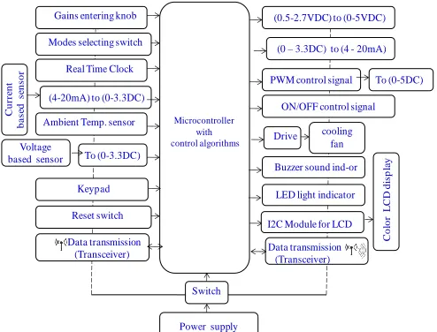
For the proposed system, the parallel design approach is applied. An ‘Arduino Due’ microcontroller is utilized as a central processor. The proposed PID and ON/OFF controllers are implemented for the LED light intensity control. The proposed control unit exhibits following features: (a)__________________________________
5200
Operating on 3.3V direct current (b) allowing to accept inputs of both current and voltage sensors’ i.e.; current (4 to 20 mA) and voltage (0 to 5 VDC) or (0 to 3.3VDC) respectively; A signal conditioning circuit for converting the current to voltage. (c) The proposed unit is developed to generate four different types of the control signals; (1), continuous (0 to 5 VDC) or (0 to 3.3VDC), (2) PWM (0 to 255) signal, (3) current (4 to 20 mA) signal and (4) fully ON/OFF signal. Control designer uses a switch or a keypad to select the best control algorithm for specific physical application. (d) Designed with both direct wire and wireless interfacing communication. (e)For heat dissipation, the unit is designed with heat sink, housing with slots for air circulation and cooling fan. For ON/OFF switching, the cooling fan and the noncontact NTC temperature sensor is used as part of control unit design. (f) Designed with LCD for visual data display (values of; S.P., gains’, error, selected control mode, selected control signal type, volts or PWM, a control signal, time). (g) Designed with Light and soft sound Indicators. (h) C compiler is used to program the microcontroller. (i) The block diagram representation and components layout of the suggested control unit design is shown in Figure 1. The suggested control unit with these features is physically developed, tested and the results are presented in this work.
3. SYSTEM HARDWARE
To develop the suggested control unit design physically and its testing in real-life applications, the following hardware components are required; Microcontroller, hardware for components interfacing, plugin and data entering (e.g. switches, Adapter Jack), signal conditioning, power supplies, housing with slots, data displaying LCD, sensor for reading process variable(s), wireless communication module between control unit, sensor and actuator’s drives, cooling heat sinks and fan. Each of the aforementioned components is given, in the next sub-sections of this manuscript, to be selected, designed, sized, and integrated into the overall control unit’s suggested design.
3.1 The microcontroller
Among the existing microcontroller types of Arduino boards Arduino Due, as of its best features, is used in current study for the suggested control unit design. Arduino zero board can also be utilized but Arduino Due is preferred as of its features. The Arduino Due board is developed based on the Atmel SAM3X8E ARM Cortex-M3 CPU. It is a 32-bit ARM core microcontroller. It has 54 digital input/output pins (of which 12 can be used as PWM outputs), 12 analog inputs, 4 UARTs (hardware serial ports), an 84 MHz clock. [9-11] Arduino Due board is shown in Figure 2.
Microcontroller with control algorithms Real Time Clock
Power supply Reset switch
Keypad
Switch
Data transmission (Transceiver) (0.5-2.7VDC) to (0-5VDC)
Drive cooling fan LED light indicator Buzzer sound ind-or Ambient Temp. sensor
Data transmission (Transceiver) (4-20mA) to (0-3.3DC)
Gains entering knob Modes selecting switch
PWM control signal ON/OFF control signal
C
u
rr
en
t
b
a
se
d
s
en
so
r
To (0-3.3DC) Voltage
based sensor
(0 – 3.3DC) to (4 - 20mA)
I2C Module for LCD
C
o
lo
r
L
C
D
d
is
p
la
y
To (0-5DC)
Figure 1: The block diagram representation and components layout of the suggested control unit design.
3.2 Components for interfacing and data inputting/outputting.
For data input and hardware components interfacing/plug in/wiring, components such as control knobs, keypad, DC jack, 4x4 keypad and rotary angle sensor, non-Contact NTC temperature sensors are utilized. All these selected components are shown in Figure 3 (a-e) Data input values
may include but not limited to sensor’s readings, Gains’
selection, set point, ambient temperature reading, control algorithm mode selection and password.
Figure 2 Arduino Due board [11]
Figure 3 (a) DC barrel 2.1mm jack
Figure 3 (b) Rotary angle for selecting gain values
Figure 3 (b) 4X4keypad
Figure 3 (d) Control knobs
Figure 3(e) Non-contact NTC Temperature sensor
3.3 Interfaces, signal conditioning, and power supplies.
The hardware components as shown in Figures 4(a-j), are required and selected to be interfaces between components and as HMI; (a) DC power interface for powering microcontroller, switches including; SPST Mini Rocker lighted Switch 6-12V for switching ON/OFF the whole system and mini push button switch for resetting. (b) Three Regulator Modules, types; (1)3.3V Regulator Module, with input 4.5-12 DC. AMS1117, (2) 5V Regulator Module, with input 4.5-12 DC and (3) Adjustable DC Voltage Regulator Module, Output
Voltage: ~1.2-37V Vin -3V (4.2V-40Vin) with Output of 5 VDC
at 1A. (c) LCD 16x4 Character Display Module, and I2C
AT24C32 Module (RTC Module).(f) High-intensity light and soft sounds Indicators.
Figure 4 (a) Mini Push Button Switch.
Figure 4 (b) DC power interface.
Figure 4 (c) SPST Mini Rocker Switch 6-12V
Lighted.
Figure 4 (d) voltage regulator.
Figure 4 (e)Adjustable DC Voltage Regulator Module ,
Figure 4 (f)Current to Voltage converter
Figure 4 (g) LCD (Character 16x4)
Figure 4 (h) Transceiver NRF24L01module
Figure 4 (i) Real-Time Clock Module
Figure 4 (j) high-intensity light and soft buzzer
Indicators
3.3.1 I/O ports, signals readings, processing, and conversion.
Two input signal types are to be read and displayed i.e. voltage and current. The Atmel SAM3X8E Arduino Due analog input pin is designed to sense small-signal values in terms of voltage. The smallest step size of readings, for 10 bit
Arduino Zero board is210=1023 and for 12 bit Arduino Due
board is 212=4095. For Arduino board, that operates on a voltage range (0 to 5 VDC), the smallest step size of readings, is calculated as given in Eqs. (1, 2):
Readings step size =5/210 = 5/1023 = 0.00488volts (1)
Readings step size =5/212 = 5/ 4095 = 0.00122volts (2)
3.3.2 Reading and converting voltage signals into desired tolerant level.
The Arduino Due is developed based on Atmel SAM3X8E microcontroller that has 12-bit ADC capabilities; this will convert input readings into values between 0 to 4095. (a) Sensors with outputs range (0 to 3.3 VDC) are read to control unit, directly by any of 12 analog input ports. (b) For sensors with outputs range (0 to 5 VDC), there exist different ways to drop voltage to (0 to 3.3 VDC), including; (1) configuring an op-amp with gain of 2/3, (2) using a voltage divider circuit to scale a (0 to 5VDC) signal down to (0 to 3.3 VDC), the circuit
is shown in Figure 5. The values of resistors R1 and R2 are
calculated by Eq.(3)
Vout = Vin * (R2 / R2 + R1) (3)
3.3.3 Industrial field instruments current signals conversion to voltage signal
Industrial field instruments (transmitter) use three or two-wire (4 to 20 mA) current loop for both power and signal output. On the other hand, most control units and data acquisition devices are designed to accept voltage signals e.g. between 0 to 3.3 and 0 to 5 VDC. For case (1): The selected microcontroller for the control unit accepts voltage range (0 to 5 VDC).The circuit for converting industrial field instruments’ (sensors’) output (4 to 20 mA) current signal, into (1 to 5 VDC) voltage signal, is shown in Figure 6(a). In this circuit, to
convert (4 to 20 mA) current into a voltage, Ohm’s law is
applied as given in Eq.(4), parallel resistor is placed between sensor’s output signal and ground. Moreover, converting and filtering circuit (shown in Figure 6(b)) is better to be applied. The value of the parallel resistor is found by Eq. (3). Further software integration is applied to convert, by mapping, the resulted voltage from (1 to 5 VDC) to (0 to 5 VDC). For case (2): the selected microcontroller is designed to accept voltage range (0 to 3.3 VDC). The value of the parallel resistor is calculated by Eq.(4) to be 165 Ohms. For application in sensing instruments, wire wound or metal film resistors are preferable. Other option for converting the current signal into voltage, include, integrating the design with current to voltage converter module for two and three wires current sensors as shown in Figure 6(c)(d).
R=V/I = 5/0.02= 500/2 = 250 Ohms (4)
Figure 5 voltage divider circuits to scale down a (0 to 5VDC) signal from sensor to (0 to 3.3 VDC)
Figure 6(a) Circuit for Converting current signal
Figure 6(b) circuit for signal converting & filtering.
Figure 6 (a,b) circuit for converting sensor’s output (4 to 20
mA) current signal into (1 to 5 VDC) voltage signal.
Figure 6(c) current to voltage converter module
for 2 wires sensor
Figure 6(d) current to voltage converter module for 3 wires
sensor
5202
Figure 6(e),the 4-20mA-T Click board
Figure 6(f) 20 mA current to voltage converter module p7711
Types of the output control signal: The suggested control unit design is developed to generate four different control signal types; continuous voltage (0 to3.3VDC and 0 to 5VDC), Current (4 to 20 mA), PWM ( 0 to 255) and fully ON/OFF Output control signal types.
3.3.1.4 Generating continuous output control voltage signal with two ranges (0 to 3.3 VDC) and (0 to 5VDC): Different options are available; (a) using Arduino board that has a built-in Digital Analog Converter DAC, to generate contbuilt-inuous output voltage (Arduino Due and zero boards are generating (0.5 to 2.7 VDC), (b) an external DAC chip can be used to create the analog continuous voltage, a good option is using chip the MCP4821/2, (c) converting PWM signal into continuous voltage signal. For the case (a) the selected Arduino Due board is generating output continuous signal in the range (0.5 to 2.7 VDC). This value is calculated as follows; Arduino Due board has an analog output voltage from (1/6 = 0.1667 to 5/6 of the reference voltage, that can
have the following values Vref = 3.3 V or 5 VDC. For
reference voltage Vref = 5VDC, the analog output voltage is
from ((1/6)*5 = 0.8334 V) to ((5/6)*5= 4.167 V).
For Vref = 3.3 VDC the analog output voltage is from ((1/6)*3.3
= 0.55 V) to ((5/6)*5= 2.75V).
For 12 bit (212 = 4095 ) digital to analog converter DAC, the
generated output voltage range is only as given by Eq.(5) with a resolution as given by Eq. (6).
Output range = 2.75 - 0.55 = 2.2 V (5) Output resolution = 2.2 /4095 = 0.5372 mV (6)
The circuit setup for converting and amplifying the (0.5 to 2.7 VDC) output control voltage signal value to reach the desired value (0 to 5 VDC) is shown in Figure 7(a), here a simple differential amplifier, realized with an op-amp, is used. The differential amplifier has gain value as given by Eq.(5), with R1 = 100k, R2 = 226k (using standard values), and powering the amplifier’s pin 8 of U1 (amplifier is shown in Figure 7 (a)) with a minimum of 7 volts. In case, the desired output voltage range is between (0 to 3.3V), the differential amplifier gain value is calculated to be G = 3.3 /2.2 = 1.5. Components to be used to build the circuit are: Resistors with a tolerance of 1% or less, Operational amplifier (e.g. LM358) suitable for single-supply is to be used (not LM741, LM1458, and TL081), also, in this circuit, need to avoid long wires.
G= 5/2.2 = 2.27 =R2/R1 (5)
Figure 7(a) The circuit for converting and amplifying the output voltage from (0.5 to 2.7 VDC) into (0 to 5 VDC) [12].
3.3.1.5 Generating continuous output control current signal (4 to 20 mA) range: different options are available to convert continuous analog (0.5 to 2.7) voltage signal into current (4 to 20 mA). One option is by converting the output analog signal from (0.5 to 2.7 VDC) into analog either (0 to 3.3 VDC) or (0 to 5 VDC), that is converted into current (4 to 20 mA) signal using voltage to current conversion module shown in Figure 8(a). 3.3.1.6 Converting PWM signal into continuous current or voltage signal; different options are available, including; using a low-pass filter on a PWM output pin. Another option using the 4-20mA-T Click board shown in Figure 8(b). by this module, the output PWM signal (0 to 255) is converted into (4 to 20 mA) continuous current signal. Furthermore, and as an alternative option, this current signal can be converted into continuous control (0 to 5 VDC) voltage signal using module 20 mA current-voltage converter module p7711 shown in Figure 8(c).
Figure8(a) voltage to current (4 to 20 mA) converter
Figure 8(b) the 4-20mA-T Click board
Figure 8(c) 20 mA current voltage converter module p
7711
3.4 Mechanical structure outer housing design
The housing and outer design for the control unit are to be designed to enclose all components, to include slots and fixtures to fix and hold hardware components, and to interface and wire sensors and drives, light and sound indicators, HMI and others.
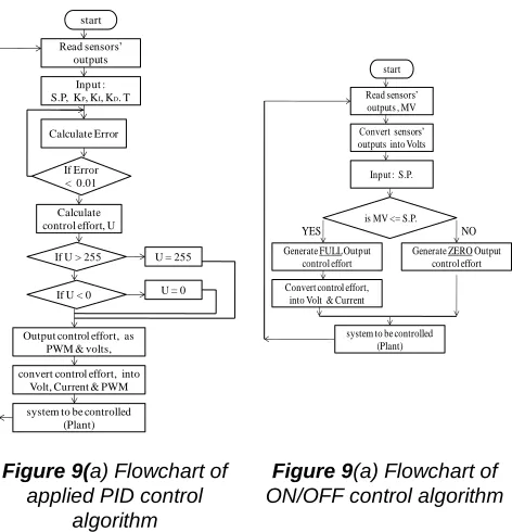
3.5 Control Algorithm design
The two applied control algorithms are ON/OFF and continuous PID- ( P-, PD-, PI-, PI-D) modes. Flow charts, shown in Figure 9(a), are used to conduct these two algorithms design. In Figure 9(a) is shown the flowchart of
applied PID control algorithm, including; reading sensors’
derivative = (error - previous_error)/dt;
control effort.= KP*error+ KI*integral + KD*derivative;
To conduct the ON/OFF control algorithm, the flow chart, shown in Figure 9(b), is used.
start
Read sensors’ outputs
Input : S.P, KP, KI, KD. T
Calculate Error
Calculate control effort, U
If Error < 0.01
If U > 255 U = 255
If U < 0
Output control effort, as PWM & volts,
convert control effort, into Volt, Current & PWM
U = 0
system to be controlled (Plant)
start
Read sensors’ outputs , MV
Input : S.P.
is MV <= S.P.
Generate FULLOutput control effort
Convert sensors’ outputs into Volts
Convert control effort, into Volt & Current
system to be controlled (Plant) YES
Generate ZERO Output control effort
NO
Figure 9(a) Flowchart of applied PID control
algorithm
Figure 9(a) Flowchart of ON/OFF control algorithm
4. System Prototyping, Testing, and Evaluation
To test the suggested control unit design in action for real-life applications and scenarios, the selected and designed hardware components were integrated to produce overall one system, as shown in Figure 10.
N T C te m p G ai ns inp ut ti ng
RTC Res
et S SPST Voltage Regulator vol ta ge to cur re nt P W M int o cur re nt 4 to 20 mA cur re nt to v ol ta ge 0 to 5 V D C 4 to 20 mA 0.5 t o 2 V .7i nt
o 0 t
o 5 V D C 0 to 5V int o 0 to 3.3 V cur re nt t o vol ta ge Transceiver M od e se le ct ion S Power supply P W M s igna l
Figure 10 The integration diagram of all hardware physical components in one system prototype
4.1 Testing and evaluation of the developed circuits, modules, signals generating, processing and outputting
In this section, the testing, analysis and evaluation process of
input and output signals’ values are introduced. Their types
and magnitude including signals reading, conversion,
modification, amplification,, processing-decision making, signal generation, manipulation and output are also mentioned.
4.1.1 Signals inputting to control unit
The system is designed to read/input two signal types; voltage and current.
(a) For the case read/input voltage signal type, there are two voltage ranges (0 to 3.3 VDC) and (0 to 5 VDC). Sensors with outputs range (0 to 3.3 VDC) are read to Arduino Due to based control unit directly by any of the 12 analog input ports. For sensors with outputs range (0 to 5 VDC), voltage divider circuit, as shown in Figure 11(a), is developed to drop sensor’s readings from (0 to 5 VDC) to (0 to 3.3 VDC)
compatible with Arduino Due, with resistors’ values (e.g. R1
=1000 Ohm , R2= 1950 Ohm). Potentiometer was used as
analog sensor to output signal between (0 to 5 VDC), this signal was input to voltage divider circuit, both, sensor output signal and output of voltage divider signal was read to Arduino Uno and displayed using Arduino serial monitor, the developed circuit, testing, reading and converting results are shown in Figure 11(b).
(b) For the case read/input current signal type the (4 to 20 mA) current signal, most of the industrial transmitters are generating current output signal between (4 to 20 mA). as discussed, different options are available to convert this current signal into DC voltage signal with value between (0 to 3.3VDC) to be read to microcontroller; the first option is applying Ohm’s law and wiring parallel resistor value of 165 Ohms, as discussed and explained in Figure 6(a)(b). The second option is utilizing current to voltage e.g. shown in Figure 8(c).
4.1.2 Signal generation, processing and output from the control unit.
The system is designed to generate four output signal types, in particular; voltage of two ranges (0 to5VDC) and (0 to 3.3VDC), current (4 to 20 mA), PWM (0 to 255) and fully ON/OFF signals (0/5VDC).
5204
module, the circuit setup and conversion results are shown in Figure 12(c).
(c) For the case of converting PWM signal into continuous current or voltage signal;, different options are available for this case, including the next three options; (a) using a low-pass filter on a PWM output pin. (b) Using the 4-20mA-T Click board as shown in Figure 8(b), by this module, the output PWM signal (0 to 255) is converted into (4 to 20 mA) continuous current signal. (c) Furthermore, and as an alternative option, this current signal can be converted into continuous control (0 to 5 VDC) voltage signal using module 20 mA current-voltage converter module p 7711 as shown in Figure 8(c).
0 to 5 VDC
0 to 3.3 VDC 3.3
5
Figure 11(a) Figure 11(b)
Figure 11(a, b) the built circuit and testing results of reading and dropping pot analog signals from (0 to 5VDC) range to (0
to 3.3 VDC) range using a voltage divider
Figure 12(a) The built circuit and set up for reading and amplification of (0.5 to 2.7 VDC) signal into either (0 to 5
VDC) or (4 to 20 mA) signal
Figure 12(b) Results of amplifying controller’s continuous output voltage signal from (0.5 to 2.7 VDC) into continuous signal between two ranges (0 to 3.3 VDC) and (0 to 5 VDC)
values ( the signals’ values are scaled 1:2)
current (4 to 20 mA)
Figure 12(c) converting controller’s continuous output voltage
signal (0.5 to 2.7 VDC) into current (4 to 20 mA)
4.2 Testing and Evaluation of the control unit and signals
(a) Controlling the angular position; Potentiometer was used as angular position sensor to sense the position in the range
(0o to 90o) degrees, and generate in turn voltage signal in the
range (0 to 5 VDC), this signal was dropped to (0 to 3.3 VDC) acceptable by control unit, using circuit as shown in Figure 11(a), this voltage was input to designed control unit, mapped using control algorithm, to output control voltage signal in the range (0.5 to 2.7 VDC). The built circuit, the generated inputs and results as output signals are shown in Figure 13(a and b). To read and display the results, generation and conversions of the voltage signal in the range of (0-5 VDC), in addition to Arduino Due, Arduino Uno and mega was used.
Figure 13 (a)
0 to 5 VDC 0 to 3.3 VDC 3.3
5
0.5 to 2.7 VDC 2.7
0.0
Figure 13 (b)
Figure 13 (a.b) controlling the angular position; (a) the built circuit, (b)signal reading, dropping, inputting to
control unit, processing and outputting
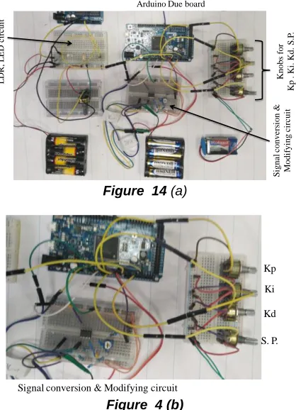
(b) Controlling the brightness of high intensity LED: The simple circuit for controlling the brightness of high-intensity white LED, using LDR as a light intensity sensor was built. In this setup, the LDR with voltage divider circuit, was built to measure light intensity and output voltage signal in the rage (0 to 5 VDC), this value was mapped by circuit as shown in Figure 7(a) to (0 to 3.3), then input to control unit with PID control algorithm, four potentiometers were used to define
and input the values of PID gain (KP, KI, KD) and Set point
S.P. In addition to Arduino Due, Arduino Uno and mega was used to read and display modified signals. The physical setup is shown in Figure 14 (a and b). The testing results in terms of signals values, conversion and output, selected gains values are mentioned. Sensor input voltage value, output control voltage signal, error signal, and set point, are also discussed below.
Test (1): Testing the system, with PID gains set as; KP =15,
KI= 0.01; KD= 6, and with desired brightness level, set point
S.P.=4, with maximum brightness level equal to 5, resulted in response curves as shown in Figure14 (c), and numerical values are listed in Table 1
Test (2): by improving the PID gains to reduce error and
speed up the system, by setting PID gains as; KP =3, KI=
0.01; KD= 4, with S.P.=4. This resulted in improved response
curves as shown in Figure 14 (d), and numerical values are listed in table 1.
Test (3): by improving the PID gains by setting as; KP =1, KI=
0.01; KD= 2, with S.P.=4. This resulted in response curves as
K
nobs
for
Kp
.
Ki
.
Kd
.
S
.P
.
Arduino Due board
L
D
R, L
E
D
c
irc
ui
t
S
igna
l
c
onve
rs
ion &
M
odi
fyi
ng
c
irc
ui
t
Figure 14 (a)
Kp
Signal conversion & Modifying circuit
Ki
Kd
S. P.
Figure 4 (b)
Figure 4 (a)(b) control unit set up; controlling the brightness of high-intensity white LED, using green LED and /or LDR
PID Control signal 24
2.3
Actual Brightness
4 S.P.
Error -1.3
Figure 14 (c) Test(1): Response curves for controlling the brightness level
24
PID Control signal
Actual Brightness S.P.
Error -1.3
4
2.3
PID Control signal Error
Figure 14 (d) Test (2): Response curves for controlling the brightness level:
PID Control signal
Actual Brightness
Error S.P.
24
2.3 4
Figure 14 (e) Test (3): response curves for controlling the brightness level
Table 1: Testing results Test
No S.P. KP KI KD
E
Effort (final)
Settling Ts
(1) 4 5 0.01 6 -1.3 24 -
(2) 4 3 0.01 3 0 0 12
(3) 4 1 0.01 2 0 0 1.5
5. CONCLUSIONS
In this work, the main goal was to utilize the modern scientific interdisciplinary advances, to suggest, build and program a new modified design and form with advanced capabilities of microcontroller-based control unit utilizing different control algorithms. The theoretical design and physical prototype of a new microcontroller-based control unit design utilizing continuous control algorithms has been presented. The system is designed to read two types of signals; voltage and current and to generate four types of signals; voltage, current, PWM and Fully ON/OFF, enabling the design to be applicable in both consumer and industrial applications. The designed special circuits and selected electronic modules were built, integrated and successfully tested to process control. The developed prototype was successfully tested and the experimental results are discussed. As future work, current readings, processing, and transmission will be experimentally tested and evaluated by applying electronic circuits and modules.
6 REFERENCES
[1] Dsign of a General Purpose 8-bit RISC Processor for
Computer Architecture Learning, ‘Antonio Hernández Zavala , Oscar Camacho Nieto , Jorge A. Huerta Ruelas, Arodí R. Carvallo Domínguez ‘,Computación y Sistemas, Vol. 19, No. 2, 2015.
[2] Alpesh Kumar Dauda, Nalinikanta Barpanda,
Nilamani Bhoi, Manoranjan Pradhan , Control Unit
Design of a 16-bit Processor Using VHDL
‘International Journal of Advanced Research in Computer Science and Software Engineering’, Volume 3, Issue 12, 2013.
[3] May Thu Win, Than Nwe, Nay Win Zaw, ‘Design and
5206
[4]Man, L. R., Ching, L. H. , "Sustainable Smart Home
and Home Automation: Big Data Analytics Approach", International Journal of Smart Home, 10 (8). 2016.
[5]Erham. E , Markus A. W P Sopianti, ‘Design of a new
on-off controller based on Arduino UNO R3 with application to Window A/C ‘,IPTEK journal of proceedings series , 2008.
[6]Kanoria Shubham Anil, Pandya Jeet Madhusudan,
Priyam Anilkumar Parikh, ‘Design and Development of Universal Motor Control Unit using MATLAB and Arduino’, National Conference on Emerging Trends, Challenges & Opportunities in Power Sector, International Journal for Scientific Research and Development (IJSRD/Conf/ ETCO2017 /2017/019.
[7]Akinwole OO, Oladimeji TT (2018) Design and
Implementation of Arduino Microcontroller Based Automatic Lighting Control with I2C LCD Display. J Electr Electron Syst 7: 258. DOI: 10.4172/2332-0796.1000258.
[8]Instruction Manual, "CONTROLLINO" MINI, MAXI and
MEGA", CONELCOM GmbH Trientlgasse 18c 6020 Innsbruck / Austria.
[9]May Thu Win, Than Nwe, Nay Win Zaw, ‘Design and
Implementation of Elevator Control System by Arduino Microcontroller ‘,International Journal of Science, Engineering and Technology Research (IJSETR) Volume 7, Issue 12, 2018.
[10] Man, L. R., Ching, L. H. , "Sustainable Smart Home
and Home Automation: Big Data Analytics Approach", International Journal of Smart Home, 10 (8), 2016.
[11] Man, L. R., Ching, L. H. , "Sustainable Smart Home
and Home Automation: Big Data Analytics Approach", International Journal of Smart Home, 10 (8), 2016. ‘
[12]
![Figure 7 (a) The circuit for converting and amplifying the output voltage from (0.5 to 2.7 VDC) into (0 to 5 VDC) [12]](https://thumb-us.123doks.com/thumbv2/123dok_us/8642717.1432425/4.612.352.527.61.183/figure-circuit-converting-amplifying-output-voltage-vdc-vdc.webp)