Wafer-Level Charged Device Model Testing
Bruce C. Chou (1), Timothy J. Maloney (1), Tze Wee Chen (2)
(1) Intel Corporation, 3601 Juliette Lane, Santa Clara, CA 95054 USAtel.: 408-765-8435, e-mail: [email protected] (2) Stanford University, Stanford, CA 94305 USA
This paper is co-copyrighted by Intel Corporation and the ESD Association
Abstract – Charged Device Model (CDM) ESD testing is demonstrated on wafer level. With a custom
probe-mounted printed-circuit board and a high-frequency transformer that captures fast CDM pulses, wafer-level CDM (WCDM) pulses are applied and monitored repeatably. Modeling of CDM and WCDM in the time and frequency domain illustrates the dominant effects, and shows that WCDM can reproduce all the major phenomena of package-level CDM testing.
I. Introduction
Charged Device Model (CDM) ESD events happen during the mechanical handling of integrated circuits, and have often caused device failure [1]. As a result, CDM testers have been developed to test the effectiveness of the ESD protection circuitry. Among them, the nonsocketed CDM (ns-CDM) tester was developed to duplicate real CDM events as described by both the ESD Association and JEDEC [2,3]. The ns-CDM tester, according to [4,5], can be circuit modeled as in Figure 1 and the immediate charge packet Qimm can be calculated. In Figure 1, Cfrg is
approximately the capacitance from the ground plane to the field plate. Cf is the capacitance of the device under test (DUT) to the field plate, and Cg is the capacitance of the top ground plan to the DUT. A CDM event happens when the discharge pin makes contact with DUT, thus closing the switch. The resulting Qimm is
. *
2 1 Q
Q Cfrg Cf
Cfrg Cf Cg Cf Cg
Cf Vf
Qimm ⎥= +
⎦ ⎤ ⎢
⎣ ⎡
+ + ⎥ ⎦ ⎤ ⎢
⎣ ⎡
+
= (1)
This circuit model has shown close agreement with charge packet measurement done through the 50-ohm line shunting the 1-ohm disk resistor.
The equation above can be simplified without altering the sum if certain conditions hold. Usually, because of the thin dielectric, Cf >> Cg, which implies that Q1 << Q2. It also means the quotient Cf/(Cg + Cf) ≈ 1. We are left with the following equation
).
||
(
Cf
Cfrg
Vf
Q
imm≅
⋅
(2)Figure 1: Circuit model for a field-induced ns-CDM tester. Switch closes when the discharge pin hits the DUT.
In a recent study [6,7], a charge instrument, built on a small PC board, that simulates the ns-CDM circuitry is introduced to simulate the action of a charged component touching grounded factory equipment. The schematic diagram of the charge instrument is shown in Figure 2.
The Qimm of the charge instrument relates to its
equivalent capacitance Ceq through
.
eq
imm hiV C
Q = ⋅ (3)
The Qimm of the charge instrument can thus be set to
equal that of a ns-CDM tester through capacitance and voltage. The small PC board with the charge circuitry now inspires a new application, whereby the board is equipped with a point probe and a viewing hole to perform WCDM testing on a probe station. This paper describes WCDM test setup and provides circuit-level analysis and data to confirm the validity and repeatability of the CDM waveform generated.
II. WCDM Setups
The charge instrument described in Figure 2 is modified to allow probing as follows. To probe wafer-level pads, the discharge peg is replaced with a probe tip. A viewing hole around the probe tip allows viewing the pads through a microscope from the probe station.
Using
C
≈
ε
⋅
A
/
d
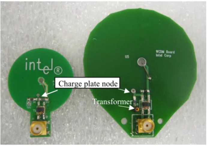
, one can modify either the area of the charge plate on the WCDM board or the length of the bent probe tip to adjust the capacitance. Varying the area with two different sized boards is shown in Figure 3, one at about 5 pF and one around 15 pF, to cover a wider range of charge packet and peak current.Figure 3: WCDM boards top view. Left-hand board is 32 mm diameter and is made from the charge instrument. Charge plate is in bottom layer, connected through the charge plate node.
The probe tip used is the PTT-120, 12 um radius tungsten needle from Cascade Microtech. This size probe tip caused no significant pad erosion due to the CDM spark. A metal jig assures consistent bending of probe tips. A 100 Mohm series resistor replaces the 1 Mohm in Figure 2 to better correlate with the 300 Mohm in ns-CDM.
To minimize recharge pulses and leakage current after a discharge, a triac grounds the voltage supply at that time. The triac (NTE5620, 800V, or CTA06, 1kV) is triggered from the oscilloscope trigger-out as soon as the discharge is sensed. The control circuit is easily reset using a pushbutton switch. The control circuit, built separately in a portable box, is shown in Figure 4. The total time it takes for the triac to turn on is around 420 ns.
Figure 4: Triac controller circuit.
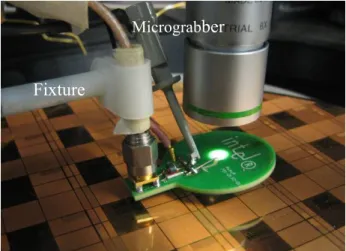
Using a fixture that ties the board to a positioner, it is possible to move the WCDM board in x, y, and z direction to test a desired I/O pad. A typical measurement setup is shown in Figure 5.
hiV source
Wafer Chuck
WCDM board Probe holder
Probe Station Controller box
(triac logic)
Oscilloscope
Attenuator (if needed)
Fixure Trigger out
Microscope SMA to BNC
Charge plate node
Transformer
Figure 5: WCDM setup on a sample probe station.
Analyzer (SPA). Figure 6 shows the setup for IV measurement.
Figure 6: WCDM setup for curve tracing.
Now, let us compare circuit models for the CDM and WCDM test setups.
III. CDM Tester Model
The essential ESDA or JEDEC CDM test circuit can be modeled as a single LRC series loop as long as certain parasitic elements are negligible. Let us first look at a more complete, yet simplified model for the CDM tester, with the aim of showing how a wafer-level tester can be set up to duplicate CDM phenomena as observed on packaged devices.
Various references on CDM testers [4, 7-8] have shown the utility of a 3-capacitor model of the device in the tester, and that a series-parallel combination of the three capacitors can be used to extract a single equivalent device capacitance Cimm for the resulting
fast event. Then for field plate charge V0, the
immediate charge is Qimm=CimmV0. The main resistive
element in the circuit is the spark resistance Rs, which can vary considerably and is also time dependent [9], but a typical deduced value for the CDM tester might be 25 ohms. That leaves the inductance, which appears mostly in the test head pogo pin probe [9] and the packaged device itself. In order to match the required waveform, the JEDEC CDM test head has extra electrical length, either because of an inductor, or because the 1 ohm current detecting resistor, feeding the 50 ohm scope cable, is recessed behind a small cavity. Also, the packaged device can have up to 2-3 cm of trace length from the pin to the die for large packages. Signals on these traces may be impedance matched to 50 ohms all the way to the die, but in the ESD regime, diodes or other highly conductive protection devices turn on and reduce the terminating impedance to low numbers of ohms.
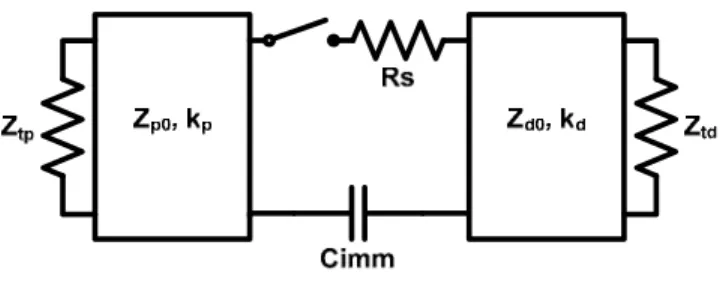
Thus we have transmission lines on either side of the spark resistance and switch. Before returning to the transmission line model, let us picture those 1-ohm-terminated transmission lines as equivalent T-networks as shown in Figure 7, in order to focus on the principal RLC poles and zeros of the network. Micrograb
ber
Fixture
Figure 7: CDM testing equivalent circuit, with (charged) device circuit on the right and (grounded) test head and probe on the left. Rp = 1 ohm is the test head current detector and Rd ≈ 1 ohm is the on-chip protection.
In Figure 7, the charged (hot) side, with the device
model, is on the right and the grounded side, with the pogo pin and test head model, is on the left. The related approximate values of Cp and Lp for package options, calibration fixtures and test head options are shown in Table I. Our principal concern is the outer loop of Figure 7, which is reducible to the well known series LRC. It has two poles and a zero in the admittance function, and resistance dominated by the spark. This admittance function is
, 1 )
( 2
+ + =
RCs LCs
Cs s
Y (4)
where the L,R, and C values are clear from the totals in the outer loop.
The usual observation, particularly on oscilloscopes of 1 GHz bandwidth or less, is of a single sharp spike and limited or nonexistent ringing, indicating an overdamped or slightly underdamped solution. This is the outer loop current through the 1 ohm detector. But note that the effective capacitances of the transmission lines form inner loops, all with the same resistor Rs, on each side of the circuit. This introduces several options for high frequency poles, as the device or probe capacitors bypass some of the outer loop inductance. These new poles are manifestly at higher frequency than the outer loop because of the lower inductance, and the series capacitance with Cimm. Thus we have the
reported when multi-GHz measurement systems are used [10], and not seen for lower-frequency measurements where the outer loop alone is visible. Note that all of these complex resonant frequencies depend on the interaction between the test head and the device under test; if the device trace length is changed, all the poles will move. Thus it is no surprise that peak currents (and much else) vary with package location [11], even aside from the Cimm
variations due to field plate and ground plate movement. As the calibration fixtures each have few parasitics of note, and a stable Cimm, they should work
as intended for checking out the CDM test head. The entries in Table I for Figure 7 also make it clear
why there are occasional problems with devices tested on the JEDEC CDM test head of note—the longer electrical length in JEDEC creates higher parasitic inductance and capacitance than the ESDA head. This lowers the outer loop frequencies a little, but those are already heavily modulated by Cimm. This
test head affects the inner loop frequencies because of its higher Lp and Cp. Note also that a loop through Cd can have low frequency for a long enough package trace, with an effect on use of the ESDA test head.
Table I. Approximate values of circuit elements as pictured in Figure 7.
Lp, nH
Cp, pF Ld, nH Cd, pF
ESDA test head 3.6 nH 0.22 x x
JEDEC* test
head 10-12 ~0.5-0.6 x x
Calibration
fixture x x small small
Device, short
trace (2mm) x x 0.5 0.2
Device, long
trace (2 cm) x x 5 2
*JEDEC test head with 1-ohm detector resistor is recessed behind a short high-Z cavity; effective electrical length of the the pogo pin probe and cavity is 2.5 cm in air, or 3 GHz resonance [10].
The admittance zeros of Figure 7 should be noted along with the poles. The two zeros are easily seen as the parallel LC tank circuits on the right and left, corresponding to quarter-wave shorts in the associated transmission lines. Stopping the current with a zero in the admittance function may not seem to be a bad thing, but both the 1-ohm detector resistor on the left, and the protection device on the right, are in the midst of those tanks. Thus each will feel some current at its own LC tank resonant frequency, even though overall
current is low due to cancellation in the tank. This means that there could be detector current that is not felt at the device and vice versa. But note that the package resonance of a long 50-ohm trace in dielectric, 2 cm as described in Table I, would be below 3 GHz (Table I is for well below quarter-wave frequency; 2 cm when dielectric √εr=1.5 is
quarter-wave for 2.5 GHz). This is below the 3 GHz frequency reported in [10] to be the JEDEC test head resonance, so it appears that between 2.5-3 GHz we have a vigorous half-wave series L-C resonator, which could easily cause destruction. Now, let’s return to the more accurate transmission line model. The CDM test system is well modeled by a loop as pictured in Figure 8, with two transmission lines in series, terminated by low-Z in each case. One line is for the device (impedance Zd0, usually 50 ohms, with
propagation constant and electrical length given by kd), and one is for the test head and probe (Zp0, kp),
with a presumed average test head impedance, upwards of 100-200 ohms depending on the test head.
Figure 8: Generalized transmission line model for CDM test system; test head and probe side on left and (charged) device side on right.
Terminations Ztd and Ztp are generalized forms of Rd
and Rp from Figure 7. The general expression for Zdin
is
,
)
tanh(
)
tanh(
)
(
0 0
0
⎥
⎦
⎤
⎢
⎣
⎡
+
+
=
s
k
Z
Z
s
k
Z
Z
Z
s
Z
d td
d
d d
td d
din (5)
and there is a corresponding expression for Zpin(s).
The admittance function for the network becomes . 1 ) ( )
( 1 )
(
s C s Z s Z R s Y
imm pin
din
s + + +
= (6)
interest. Because s is a complex frequency, σ+jω, it is important to note that these lowest frequency poles could be real and negative (overdamped), as the negative s-dependent terms balance Rs. The events in standard CDM testers will have major real components in their lowest frequency poles as a result of the short duration and subdued ringing of the pulse. The higher-frequency poles of Y(s) will occur beyond the first quarter-wave resonance, when one Zin goes
negative and (largely) imaginary, and eventually joins with the ever-smaller Cimm term to balance the other
Zin. This will happen at the lowest frequency when
both Zin functions approach quarter-wave near the
same frequency; when one moves beyond π/2, goes negative jtanθ and soon zeros out the denominator. Reducing the electrical length of one line pushes out this pole (or conjugate pair of poles, most likely) to higher frequency, but not above half-wavelength for the longer line. This higher frequency pole resonance can be destructive because the termination current (i.e, across our protection device) is raised by the high (equal and opposite) voltages appearing across both lines in series L-C resonance. It should be much more destructive than anything felt by the termination at a zero of Y(s). The lesson for CDM testers is that the electrical length (kp) of the test head and probe pushes
the half-wave resonance to lower frequency due to the combination of the test head and device. But since the package trace effect is part of the intrinsic factory CDM event, the high-frequency stress appears to be appropriate when those package conditions exist. Solving Eq. 6 for all relevant complex roots and inverting to the time domain would be very revealing, but will have to be the subject of a future study. We shall now return to Eq. 4, our basic low-frequency LCR loop, for insight into our WCDM instruments and measurements.
IV. WCDM Tester Model
The admittance function of Eq. 4 is solved to give two poles, expressed in pole-zero form in the Laplace domain as.
)
)(
(
)
(
b
s
a
s
L
s
s
Y
+
+
=
(7)In general, the poles at -a and -b are complex frequencies, but given the nature of our WCDM waveforms we will focus on poles that are real and negative, i.e., overdamped. These poles are given by
),
4
1
1
(
2
,
2C
R
L
L
R
b
a
=
±
−
(8)and our focus is where R>2√(L/C). The sign convention is chosen so that the time domain solution will be a sum of exponentials e-at and e-bt according to
Laplace transform analysis [12].
For WCDM, we have a slightly modified circuit as pictured in Figure 9, but it is essentially equivalent to Figure 7, and again we focus on its outer loop.
Figure 9: WCDM circuit. Rp≈0-1 ohm on wafer or ground plate. Probe (Lp, Cp) is small and charged; feed line to transformer (Ld, Cd) is on top of disk and shielded. For the 4-5 pF disk, the probe Lp=2.2 nH, Cp=0.06 pF, while Ld=2.9 nH, Cd=0.36 pF.
The CDM discharge current in the Laplace domain is I(s) = V(s)*Y(s), where V(s) is a step function for the switch arc, expressing the discharge of Cimm or Cdisk to
zero. This could be an infinitely abrupt step function V0/s, but we would like to build in the finite rise time
of the spark itself, irrespective of any LCR-related rise times. This is believed to be 50-200 picoseconds (10-90% rise time), which we will capture as an additional pole so that the step has a gradual exponential approach, V0(1-e-ct), c positive and real. For a
10-90% rise time τ we must take c=2.2/ τ. Our source becomes V(s) = V0/(s(s+c)) (neglecting normalization
factors) so we now have
.
)
)(
)(
(
)
(
0c
s
b
s
a
s
L
V
s
I
+
+
+
=
(9)This 3-pole model should give the “real” LCR discharge current waveform, as yet uninfluenced by the measurement system. Next we consider what we actually see on the oscilloscope as read out from the transformer.
V. WCDM Waveforms and
Models
pulse width, overshoot, and undershoot of the waveform are comparable to both JEDEC and ESDA standards [2,3].
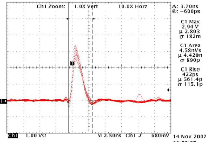
Figure 10: Typical WCDM waveform as read from the on-board SMT transformer. Small disk (4.96 pF), 100V, Tek 784D scope (1 GHz), 10X attenuator, 50 ohms. Peak current reading is 624 mA, charge is 496 pC.
Figure 11: A sample of 10 repeated WCDM waveforms. Large disk (18.5 pF), 100 V, Tek 784D scope (1 GHz), 10x attenuator, 50 ohms. connected. Average peak current reading is ~1.22 A, charge is ~1.85 nC.
One source of error with the scope waveform, particularly for the smaller disk, is the parasitic capacitance of the transformer. In Figure 12 this is pictured as a single Cpara to ground, but capacitance
across both sides of the transformer is similarly unmeasured by the scope, and the device feels it just the same. This capacitance is extracted by measuring the pulse with a 1-ohm disk resistor target in place of the wafer, as in Figure 12.
Figure 12: WCDM charge packet calibration setup.
With the two boards, a wider range of repeatable charge packet can be generated as long as the Charge-to-Voltage (Q-V) relationship is linear. The thin radius of the probe tip could limit the amount of charge the board can hold because of air ionization, but any such effect was outweighed by leakage of the 800V triac; the 1kV triac allowed charging to 1kV with little leakage of any kind. Figure 13 shows linear Q-V up to 500 V for both boards. Cpara is about
2 pF across the transformer.
Charge Packet vs. Supply Voltage
y = 0.0068x
y = 0.0047x y = 0.0131x
y = 0.0112x
0 1 2 3 4 5 6 7 8
0 100 200 300 400 500 600
Supply Voltage (V)
C
h
ar
g
e
P
acket
(
n
C
)
small_d_DUT small_d_Tx
large_d_DUT large_d_Tx
Linear (small_d_DUT) Linear (small_d_Tx)
Linear (large_d_DUT) Linear (large_d_Tx)
We will focus on the small disk in the following analysis of the WCDM waveforms.
Readout of the waveform should be influenced by the bandwidth and rolloff of the “1 GHz, 4 GS/s, 400 pS rise time” oscilloscope (Tek 784D), plus the insertion loss of the surface mount technology (SMT) transformer [13]. The latter appears to be about 3 dB/octave above about 900 MHz, and what we know about the scope indicates rolloff frequency that is almost coincident with the transformer. Accordingly, we put a measurement pole, or poles, into the function (now better described as a transfer function) at 875 MHz (=d/2π, d positive and real). To capture both the scope and the transformer, 6 dB/octave may be too little but 12 dB/octave, or two coincident poles, may capture both measurement and spark rise time effects, the latter of which are relatively minor in this measurement system. Finally, the transformer has baseline insertion loss of at least 4% at all frequencies, meaning that in calculating current and charge from voltage waveforms as in Figure 10-11, we divide by 24 ohms instead of 25. These measured values, which include the in situ measured value of
the capacitance each time, are included in the transfer function parameters. Thus our best estimate of current as measured Im(s) will be, in the 4-pole model (again
without normalization factors),
.
)
)(
)(
)(
(
)
(
0d
s
c
s
b
s
a
s
L
V
s
I
m+
+
+
+
=
(10)By developing an Excel spreadsheet, Im(s) was
converted into the time domain as a sum of exponentials e-at, e-bt, e-ct, e-dt with coefficients from
Laplace transform tables, including the Heaviside Expansion Theorem [12]. These coefficients and the boundary conditions of the problem allow normalization. For Im(s) we are using c and d to be
both at 875 MHz, plus other “reasonable” values of all parameters. We want to match the measured data such as Figure 10, and map back to plausible “real life” waveforms as in Eq. 9, by dropping out the c and d poles. Now we do this for Figure 10.
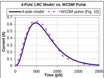
Figure 14 shows the 4-pole model for 100V discharge as determined by the following parameters:
L = 5.1 nH (estimated from probe (2.2 nH) and transformer feed line lengths and impedances)
C = 4.96 pF (directly measured, Figure 10)
R = 69 ohms (including 25 ohms through the transformer and its termination; fairly insensitive to inductance)
875 MHz=f=ω/2π, ω=1/c=1/d measurement double pole, as above.
4-Pole LRC Model vs. WCDM Pulse
0 0.1 0.2 0.3 0.4 0.5 0.6 0.7
0 500 1000 1500 2000
Time (pS)
C
u
rre
n
t (
A
)
4-pole model WCDM pulse (Fig. 10)
Figure 14: Time-domain 4-pole simulation of LRC zap, fit to Figure 10, with two-pole measurement rolloff and LRC
parameters as in the text. Peak measured current from Fig. 10 of 624 mA, and 0-peak rise time of 520 pS and other rise time features are matched. R=69 ohms implies 44 ohm effective spark resistance.
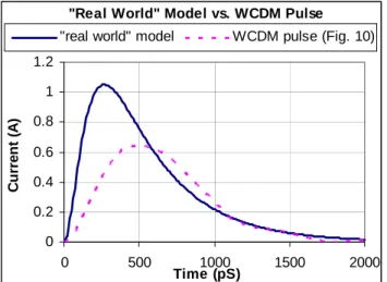
2-pole LRC solution, but with very short rise time (0-peak of 170 pS, 10-90% of 130 pS) owing to 2L/R, not very believable. Here the spark rise time is important in assessing the model. A 3-pole model with 100 pS spark rise time, 6.96 pF, and L and R parameters as in Figure 14, is shown in Figure 15. Now the peak current is 1.05 A, at 270 psec.
The 4-pole fit to measured data with the double measurement pole was adopted because it fit the scope data best on the rising edge--a single measurement pole (3-pole model, plus spark rise time) gave too fast a predicted rise time or too high a measured current when using reasonable parameter values. The deduced 1.05 A of real world peak current is convincing because it depends largely on model parameters that can be measured, or calculated accurately enough. Capacitance and voltage come from the measurement instruments, and resistance converges to 67-69 ohms over an inductance range of 3.5-5.1 nH. So the estimate of inductance does not have to be extremely accurate. When we fit the same scope data with the 4-pole model using 3.5 nH, a 45% reduction in the inductance estimate, the predicted peak current (real world, 3-pole model) rose less than 2%, to 1.067 amp.
"Real World" Model vs. WCDM Pulse
0 0.2 0.4 0.6 0.8 1 1.2
0 500 1000 1500 2000
Time (pS)
C
u
rre
n
t (
A
)
"real world" model WCDM pulse (Fig. 10)
Figure 15: Simulated “real world” current zap felt by the silicon
as measured in Fig. 10 and deduced from the model, including transformer capacitance. Peak current is 1.05 A, 0-peak rise time is 270 pS (10-90% rise time is 150 pS).
The large disk, as measured in Fig. 11, can be subjected to similar modeling. The Ipeak of 1.22 amps
happens later, after 790 psec, and the 10-90% rise time agrees with the recorded 420 psec. Because of the slower rise time, the effective R is lower, 53 ohms; thus 28 ohms is the effective spark resistance. Adding in the transformer capacitance and modeling for the “real world” pulse, as in Fig. 15 but for the large disk, we get Ipeak=1.5 amps after 440 psec, and 235 psec
10-90% rise time. Note that the corrections are much less for the large disk; only 23% higher Ipeak instead of
almost 70% higher for the small disk. As we go to press, measurements on the large disk with a 6 GHz scope (TDS 6604) show a rapid rise (180 psec, 10-90%) to 85% of the final current. The above estimates are not bad, but the transmission line and multi-element models of Figs. 8 and 9 are clearly evident with high-frequency measurements, and should be used in future modeling efforts.
These interlocking measurements and simulations give us much confidence in the WCDM instruments developed so far, and show the ability to simulate CDM phenomena much as a packaged device would feel it. The extra 25+ ohms of series resistance due to measurement, and the effectively higher Rs of the pad probe simply serve to stabilize the circuit, and can actually make the rise time faster, due to 2L/R. High peak currents and sharp, CDM-like waveforms are thus achievable by adjusting the voltage (our most easily adjustable parameter) and perhaps by having a variety of charge disks to choose from. We estimate (by solving for Ipeak in the L-C plane for given R) that
WCDM is capable of supplying Ipeak of at least 15-16
amps at 800V, with rise time matching any CDM tester, using optimized designs.
This capability and confidence in WCDM includes the transmission line model of the CDM tester-plus-device as in Figure 8. At present the line on top of the disk is 50 ohms (or slightly more for the makeshift arrangements of the smaller disk, derived from a related instrument [6]), terminated by 25 ohms and thus adding some inductance. This Ld is actually
desirable for simulating real CDM test head, cal fixture and package conditions, even though it could be tuned out completely by z-matching the 25 ohms and leaving an absurdly low inductance, and the fastest possible rise time. Note also that even the more aggressive half-wave resonance conditions of the JEDEC test head and long package traces are possible on WCDM. A deliberately long line on top of the disk (a large disk, for a large planned package), feeding a low impedance (using a step-up transformer [14]) could add the exact high frequency poles anticipated for the packaged device in a regular CDM test fixture, plus the principal low frequency poles as well. Enough WCDM instruments could test anything on wafer to feel exactly what we know it will feel when it reaches CDM testing at the package level.
a ns-CDM tester on a packaged device, with the low failure voltages shown in Table II.
WCDM testing was done for both positive and negative test voltages for both of the pins, using the smaller WCDM board. CDM failure voltage is compared with the corresponding WCDM charge packet in Table II. Voltage polarity for WCDM is reversed, to agree with current direction for the equivalent ns-CDM event.
Table II shows a consistently lower failure charge for WCDM testing, and for both methods usually a lower failure level for negative voltage. We have adjusted WCDM data for the extra 2 pF of transformer capacitance not seen by the scope. The failure voltages are in the same range for both pins and polarities; if anything, WCDM appears to have such a sharp rise time and high peak current that passing several nC should assure excellent CDM performance in a package.
Table II: Weak pin pair CDM failure comparison
ns-CDM WCDM Pad name
Voltage Charge Voltage Charge Pin A + 200 V 2.92 nC 200 V 1.43 nC
Pin A - -200 V -3.08 nC -100 V -0.73 nC Pin B + 600 V 8.64 nC 500 V 3.57 nC
Pin B - -200 V -2.76 nC -200 V -1.39 nC
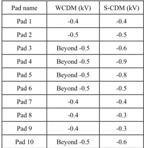
In the following test case (Table III), another known failure on a test chip is tested using a socketed-CDM tester (KeyTek ZapMaster) and reproduced using WCDM (small board, ~5 pF) to correlate.
Table III: ESD I/O pad CDM failure comparison
Pad name WCDM (kV) S-CDM (kV) Pad 1 -0.4 -0.4 Pad 2 -0.5 -0.5 Pad 3 Beyond -0.5 -0.6 Pad 4 Beyond -0.5 -0.9
Pad 5 Beyond -0.5 -0.8 Pad 6 Beyond -0.5 -0.5 Pad 7 -0.4 -0.4 Pad 8 -0.4 -0.3 Pad 9 -0.4 -0.3 Pad 10 Beyond -0.5 -0.6
Pad 11 Beyond -0.5 -0.7
Pad 12 -0.5 -0.4 Pad 13 -0.4 -0.3
The comparison above shows a strong failure correlation between WCDM testing and S-CDM testing, with a correlation coefficient among comparable pads of 0.71. However, without charge measurement of each S-CDM waveform and without measuring for WCDM failure beyond -500V, WCDM is hard to compare in depth. Also, S-CDM rise times and total charge quantities are known to be very different from ns-CDM, and now WCDM as well.
VII. Conclusions
Wafer-level CDM testing is shown to produce consistent discharge pulses comparable to the waveforms described in CDM industry standards [2,3] and CDM testers for packaged components. WCDM has become a consistent and reproducible wafer-level testing method, comparing favorably with existing CDM methods, and showing good enough correlation to build considerable confidence in the results. Discharges of a ~15 pF disk up to 1kV (~15 nC total charge) have been observed.
Simple models of CDM and WCDM in the time and frequency domain have enlightened the understanding of both kinds of tests. CDM testers can have high-frequency resonances traceable to quarter-wave and half-wave effects involving test head and package. Similar WCDM models show it to be capable of reproducing all features of package-level CDM testing, including rise times, peak currents and high-frequency resonances. The WCDM disk can also be designed with z-matching to give a clean pulse as observed in CC-TLP [15]. WCDM offers in situ
waveform monitoring and effective calibration fixtures, much as does ns-CDM.
Wafer-level testing can now be done before packaging for products, and on a wide assortment of test patterns, saving time, costs, and adding to options for evaluating ESD performance. In the future, further development of charge disks, measurement options, probing automation and waveform modeling is planned. This study has produced very positive results and has inspired us to add WCDM to our ESD evaluation toolbox.
Acknowledgments
known ESD failures and related CDM tester data. Also, Amitabh Chatterjee provided some lab data.
References
[1] P. R. Bossard, R. G. Chemelli and B. A. Unger, "ESD Damage from Triboelectrically Charged Pins," EOS/ESD Symp. 1980.
[2] ANSI-ESDSTM5.3.1-1999, “Charged Device Model (CDM)-Component Level Test Method”, ESD Association, 1999. See www.esda.org. [3] JEDEC JESD22-C101-C standard, “Field-Induced
Charged-Device Model Test Method for Electrostatic-Discharge-Withstand Thresholds of Microelectronic Components”, Dec. 2004. See www.jedec.org.
[4] R. Renninger, M-C. Jon, D.L. Lin, T. Diep and T.L. Welsher, “A Field-Induced Charged-Device Model Simulator”, EOS/ESD Symp. pp. 59-71, 1989.
[5] J.A. Montoya and T.J. Maloney, “Unifying Factory ESD Measurements and Component ESD Stress Testing”, EOS/ESD Symp. pp. 229-237, 2005.
[6] T.J. Maloney, "Instrument for Calibrating Antenna-based ESD Detectors", 1st Annual International Electrostatic Discharge Workshop (IEW), pp. 274-288, May 2007.
[7] T.J. Maloney, “CDM Protection, Testing and Factory Monitoring is Easier Than You Think”, 2007 Taiwan ESD Conference Proceedings, pp. 2-7.
[8] B. Atwood, Y. Zhou, D. Clarke, T. Weyl, “Effect of Large Device Capacitance on FICDM Peak Current”, 2007 EOS/ESD Symposium Proceedings, pp. 275-82.
[9] R. Renninger, “Mechanisms of Charged-Device Electrostatic Discharges”, EOS/ESD Symp. pp. 127-143, 1991.
[10] L.G. Henry, R. Narayan, L. Johnson, M. Hernandez, E. Grund, K. Min, Y. Huh, “Different CDM ESD Simulators provide different Failure Thresholds from the Same Device Even Though All the Simulators Meet the CDM Standard Specifications”, 2006 EOS/ESD Symposium Proceedings, pp. 343-53.
[11] A. Jahanzeb, Y.-Y Lin, S. Marum, J. Schichl, C. Duvvury, “CDM Peak Current Variations and Impact Upon CDM Performance Thresholds”, 2007 EOS/ESD Symposium Proceedings, pp. 283-88.
[12] M. Abramowitz and I.A. Stegun, Handbook of Mathematical Functions, New York: Dover
Publications, 1965.
[13] ADT1-1WT transformer, www.mini-circuits.com.
[14] Mini-Circuits, “How RF Transformers Work”, www.mini-circuits.com.