ECE 35
Spring 2017
Homework #5 Solution
All homework problems come from the textbook, “Introduction to Electric Circuits”, by Svoboda & Dorf, 9th Edition. Question numbers in the 8th edition is listed for reference.
Question Number Svoboda & Dorf, 8th Edition Svoboda & Dorf, 9th Edition
1 P 6.3-2 P 6.3-2
2 P 6.3-5 P 6.3-5
3 P 6.3-9 P 6.3-9
4 P 6.3-11 P 6.3-11
5 P 6.4-3 P 6.4-3
6 P 6.4-5 P 6.4-5
7 P 6.4-7 P 6.4-7
8 P 6.4-10 P 6.4-10
9 P 6.4-15 P 6.4-15
10 P 6.4-16 P 6.4-16
11 P 6.4-19 P 5.5-7
12 P 6.4-23 P 6.4-23
P 6.3-2 Find vo and io for the circuit of Figure P 6.3-2.
Figure P 6.3-2
Solution:
Apply KVL to loop 1:
1 1
1
12 3000 0 2000 0 12
2.4 mA 5000
i i
i
The currents into the inputs of an ideal op amp are zero so
o 1
2 1
2
2.4 mA 2.4 mA 1000 0 2.4 V
a
i i
i i
v i
Apply Ohm’s law to the 4 k resistor
o
3
4000
2.4 2.4 10 4000 12 V
o a
v v i
P 6.3-5 Find vo and io for the circuit of Figure P 6.3-5.
Answer: vo = – 15 V and io = 7.5 mA
Figure P 6.3-5
Solution:
The voltages at the input nodes of an ideal op amp are equal, so va 0 V. Apply KCL at node a:
3
0 12 0
2 10 0
3000 4000
15 V
o
o
v
v
Apply KCL at the output node of the op amp:
0 7.5 mA
6000 3000
o o
o o
v v
P 6.3-9 Determine the voltage vo for the circuit shown in Figure P 6.3-9.
Answer: vo = – 8 V
Figure P 6.3-9
Solution:
Apply KCL at node a:
a a
a 18
0 0 12 V
4000 8000
v v
v
The node voltages at the input nodes of ideal op amps are equal, so vb va.
Using voltage division:
o b
8000
8 V 4000 8000
v v
P 6.3-11 The circuit shown in Figure P 6.3-11 has one input, vs, and one output, vo. Show that the output is proportional to the input. Design the circuit so that vo = 5 vs.
Figure P 6.3-11
Solution:
Label the circuit as shown. Apply KCL at the top node of R 2 to get
s a a 2
a s
1 2 1 2
0
v v v R
v v
R R R R
Apply KCL at the inverting node of the op amp to get
2 3
4o a a 3 4 3 4 2
o a s s
3 4 4 4 1 2 1 2 4
0 R R R
v v v R R R R R
v v v v
R R R R R R R R R
We require
21 3 2
445
R R R
R R R
Figure P6.4-3
P6.4-3
Determine the values of the node voltages, va and vo, of the circuit shown in Figure P6.4-3.
Solution:
Writing node equations:
a 3
a
3 3 3
2.25 2.25
0 40 10 4.5 V
20 10 40 10 20 10
v
v
and
a a a o
o a
3 3 3
8 8 8
0 2 4.5 9 V
40 10 10 10 8 10 40 10 8
v v v v
v v
P 6.4-5 The outputs of the circuit shown in Figure P 6.4-5 are vo and io. The inputs are v1 and v2. Express the outputs as functions of the inputs and the resistor resistances.
Figure P 6.4-5
1 1 2 1 1
1 2
1 7 7 7
2 1 2 2 2
2 1
2 7 7 7
0 0 1
0 0 1
a
a
b
b
v v v v R R
v v v
R R R R
v v v v R R
v v v
R R R R
6
4 6 4 6
0 5 5
0
3 5 3 3
0
0 0
0 0 (1 )
b c c
c b
a c c
a c
v v v R
v v
R R R R
v v v v R R
v v v
R R R R
6 3 5 6 3 5 2
5 1 2 5 1
0 2 1
3 7 3 4 6 7 3 7 3 4 6 7
0 0
(1 ) (1 )
5
c
R R R R R R R
R R R R R
v v v
R R R R R R R R R R R R
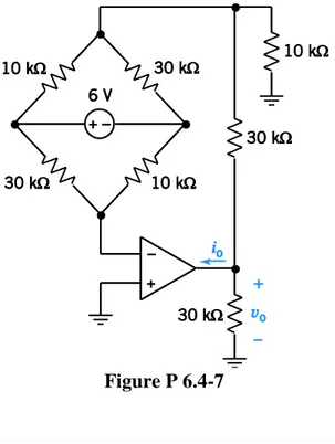
P 6.4-7 Find vo and io for the circuit shown in Figure P 6.4-7. Assume an ideal operational amplifier.
Figure P 6.4-7
Solution:
Label the circuit to account for the properties of the ideal op amp and to identify the supernode corresponding to the voltage source.
Apply KCL at the inverting input node of the op amp
a
a 0 0 6 0 0
10000 30000
v
v
or
a 1.5 V
v
a b a b
a 0 a 6 0 6 0
10000 30000 30000 10000
v v v v
v v
Multiply both sides by 30000 to get
a a a b a b
3v v 6 v v 3 v 6 v 0 Solving gives
b 2 a 6 3 V
v v
Apply KCL at node b:
a
bb b o a b 6
0 10000 30000 30000 10000
v v
v v v v v
Multiply both sides by 30000 to get
b o
a b
a
bb
3v v v v v 3 v 6 v 0 Solving gives
o 8 b 4 a 18 12 V
v v v
Apply KCL at the output node of the op amp:
o o b
o 0 o 0.7 mA
30000 30000
v v v
P 6.4-10 The circuit shown in Figure P 6.4-10 includes a simple strain gauge. The resistor R changes its value by ΔR when it is twisted or bent. Derive a relation for the voltage gain vo/vs and show that it is proportional to the fractional change in R, namely ΔR/Ro.
Answer: o o
o 1 o
R R
v
R R R
Figure P 6.4-10
Solution:
By voltage division (or by applying KCL at node
a) 0 1 0 a s R v v R R
Applying KCL at node b:
0 1 0 0 0 1 0 b s bb s b
v v v v
R R R
R R
v v v v
R
The node voltages at the input nodes of an ideal op amp are equal so vb va.
0 0 0 0
0
1 1 0 1 1 0 1 0 0
1 s s s
R R R R R R R R
v v v v
R R R R R R R R R
P 6.4-15 The circuit shown in Figure P 6.4-15 has one input, vs, and one output, vo. The circuit contains seven resistors having equal resistance, R. Express the gain of the circuit, vo/vs, in terms of the resistance R.
Figure P 6.4-15
Solution:
Writing node equations:
s 1
1 s
0
v v
v v
R R
1 1 1 2
2 1 s
0 3 3
v v v v
v v v
R R R
2 1 2 2 o
o 2 1 s
0 3 8
v v v v v
v v v v
R R R
The gain of this circuit, o
s
8
v
P 6.4-16 The circuit shown in Figure P 6.4-16 has one input, vs, and one output, vo. Express the gain, vo/vs, in terms of the resistances R1, R2, R3, R4, and R5. Design the circuit so that vo = – 20 vs.
Figure P 6.4-16
Solution:
Represent this circuit by node equations.
s a o a a
1 3 2
v v v v v
R R R
and
a o 4
o a
2 4 2
0
v v R
v v
R R R
So
s o 1 2 1 3 2 3 2
a o
1 3 1 2 2 1 2 3 4
1 1 1
v v R R R R R R R
v v
R R R R R R R R R
s 1 2 1 3 2 3 1 4 1 2 1 3 2 3
o o
1 3 1 3 4 1 3 4
1
v R R R R R R R R R R R R R R
v v
R R R R R R R R
3 4
o s
1 4 1 2 1 3 2 3
R R
v v
R R R R R R R R
We require 3 4
1 4 1 2 1 3 2 3
20 R R
R R R R R R R R
Try R1R2 R and R3R4 aR Then
2 20 3 1 a a
So a260a200
60 3600 4 80
60.332, 0.332 2
a
P 6.4-19 The circuit shown in Figure P 6.4-19 has one input, vs, and one output, vo. The circuit contains one unspecified resistance, R.
(a) Express the gain of the circuit, vo/vs, in terms of the resistance R.
(b) Determine the range of values of the gain that can be obtained by specifying a value for the resistance R.
(c) Design the circuit so that vo = – 3 vs.
Figure P 6.4-19
Solution:
(a) Use units of volts, mA, and k. Apply KCL at the inverting input of the left op amp to get
s a o
a s o
50
0 5
10 50
v v v
v v v
R R
o a s o o s
4 40 40
4 1 4
5
v v v v v v
R R
o
s
4 4
40 40
1
v R
v R
R
(b) o
s
0 R 4 v 0
v
(c) We require 3 4 120 k
40
R
R R
P 6.4-23
The input to the circuit shown in Figure P6.4-23 is the voltage source voltage vs. The output is the node voltage vo. The output is related to the input by the equation vok vs where
o
s
v k
v
is called the gain of the circuit. Determine the value of the gain k.
FigureP6.4-23
Solution:
Label the node voltages as shown. Apply KCL at the inverting input node of the op amp to get
s s a
s a a s
11
0 11 3
30000 80000 3
v v v
v v v v
Apply KCL at the right node of the 80 k resistor to get
s a o a a
s a o
s s o
s s o
o s
o s
9 4 0
80000 20000 20000
11
9 4 0
3
33 4 0
4 32
8
v v v v v
v v v
v v v
v v v
v v
v v
P 6.5-9 Determine the voltage vo for the circuit shown in Figure P 6.5-9.
Hint: Use superposition.
Answer: vo = (– 3)(3) + (4)(– 4) + (4)(8) = 7 V
Figure P 6.5-9 Solution: