UNIVERSITY OF NORTH CAROLINA CHAPEL HILL
Construction and Characterization of an
NMR Spectrometer Operating at
Earth’s Magnetic Field
by
Boris Mesits
A thesis submitted in partial fulfillment for the requirements of the Honors distinction.
under the direction of
Rosa Tamara Branca
Department of Physics and Astronomy
Declaration of Authorship
I, BORIS MESITS, declare that this thesis titled, “Construction and Characterization
of an NMR Spectrometer Operating at Earth’s Magnetic Field” and the work presented
in it are my own. I confirm that:
This work was done wholly or mainly while in candidature for a degree at this University.
Where any part of this thesis has previously been submitted for a degree or any other qualification at this University or any other institution, this has been clearly
stated.
Where I have consulted the published work of others, this is always clearly at-tributed.
I have acknowledged all main sources of help.
Where the thesis is based on work done by myself jointly with others, I have made clear exactly what was done by others and what I have contributed myself.
Signed:
Date:
UNIVERSITY OF NORTH CAROLINA CHAPEL HILL
Abstract
Advisor: Rosa Tamara Branca Department of Physics and Astronomy
Bachelor of Science
by Boris Mesits
Spin is a property of many nuclei which can be exploited for imaging and spectroscopy
with nuclear magnetic resonance (NMR) studies. While most medical applications of
NMR require large magnets to create the resonance phenomenon, the natural magnetic
field of the Earth can also serve the same purpose. Although spectral resolution is lower
due to the relatively weak field of the Earth, the continuous presence of this natural
field provides an opportunity for easy application of NMR techniques in the field.
To access this opportunity, we build and characterize the performance of a low-cost,
portable NMR spectrometer, based on the design published by Michal (2010). A
stan-dard microcontroller, fed with open-source pulse programming software from a typical
laptop, operates the experiment’s coil, removing the need for an expensive proprietary
controller. We find that the system, despite its simplicity, is susceptible to unwanted
feedback-driven oscillations in the output signal, which depends sensitively on the
lay-out of the electronic components. We show that these oscillations may be due both
to inductive coupling of ground wires to amplifier outputs, and to signal-ground
cou-pling inherent to the microcontroller. After removing the feedback-driven oscillations,
Acknowledgements
Some text and figures that appear here were previously submitted as coursework for
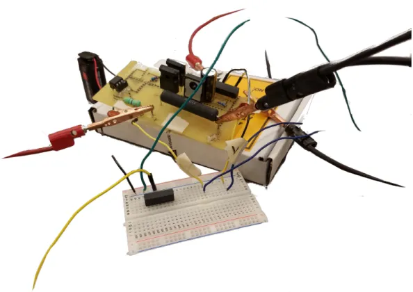
PHYS395 and PHYS691H. We note that the breadboard circuit, mentioned in the
con-clusion, was built by Nick Bryden.
I would like to thank Rosa Tamara Branca for the rewarding opportunity to focus
on undergraduate research for two years. I must also thank Michael Antonacci, Nick
Bryden, and Michele Kelly for their steady guidance during our shared time in the
laboratory. I owe further gratitude to Rose Vigil for her support and logistical assistance.
Finally I give my thanks to George Edwards, a valued colleague and a tremendous
reservoir of wires and patience.
Contents
Declaration of Authorship i
Abstract ii
Acknowledgements iii
Abbreviations vi
1 Background 1
1.1 Nuclear Magnetic Resonance . . . 1
1.2 Free Induction Decay. . . 3
1.3 Earth’s Field NMR . . . 6
1.4 Applications. . . 7
1.5 Objective . . . 7
2 Circuit Design 8 2.1 General Approach . . . 8
2.2 Microcontroller . . . 10
2.3 Transmitter . . . 11
2.4 Receiver . . . 12
3 Development and Experiment 13 3.1 In-Lab Board Manufacturing . . . 13
3.2 Professionally-Printed Board . . . 17
3.3 Calibration of Bc Frequency and Duration . . . 17
3.4 Shimming of Earth’s Field and Gradient Coil Tests . . . 18
3.5 Change in Inductance from Shielding . . . 19
3.6 Pre-Polarization of Nuclear Spins . . . 19
3.7 Compatibility of Arduino Uno and Arduino Mega. . . 20
3.8 Outdoor Experiments . . . 21
3.9 Active Shimming . . . 21
3.10 Linewidth . . . 22
3.11 Variation of Bc Duration. . . 24
Contents v
4 Hardware Performance 26
4.1 Hysteresis . . . 26
4.2 Effect of PCB Design on Feedback Oscillations . . . 28
4.3 Effect of Ground Wire Placement . . . 28
4.4 Effect of Analog Input Connections on Feedback Oscillations . . . 29
4.5 Test with Unity-Gain Amplifier on Analog Input . . . 29
4.6 Test with Second Microcontroller . . . 30
4.7 Initiation Timing of Feedback Oscillations . . . 30
4.8 Other Observations . . . 30
5 Parasitic Inductance Analysis 32 5.1 Theoretical Framework. . . 32
5.2 Numerical Implementation . . . 34
5.3 Results. . . 37
6 Conclusions 38 6.1 Feedback Oscillations. . . 38
6.2 PCB Development . . . 38
6.3 Experimental Parameters . . . 39
6.4 Note on Unusual Circumstances. . . 39
6.5 Summary . . . 40
A Validation of Induction Model 41
Abbreviations
NMR Nuclear Magnetic Resonance
EFNMR Earth Field NMR
PCB Printed Circuit Board
FID Free Induction Decay
T/R Transmit/Receive
EM Electromagnetic
AC Alternating Current
DC Direct Current
FWHM Full-Width Half Maximum
EMF Electromotive Force
MRI Magnetic Resonance Imaging
SNR Signal-to-Noise Ratio
Dedicated to my mother and father
Chapter 1
Background
1.1
Nuclear Magnetic Resonance
Nuclear magnetic resonance (NMR) is a physical phenomenon that enables some of
the most sophisticated imaging and chemical detection techniques today. [1] [2] Rapid advances in medicine followed the advent of magnetic resonance imagining (MRI), an
application of NMR physics. The non-invasive nature of NMR is of key importance
to in vivo biological studies. [3] Chemists use NMR spectroscopy to determine the composition of complex mixtures, and to monitor the progress of chemical reactions.
[2]The structure of molecules may be deduced from NMR spectroscopy as well, as in the famous example of buckminsterfullerenes. [1]
The phenomenon of NMR was first discovered in 1946 due to experiments by Felix Bloch
and Edward Mills Purcell. [1] They detected the NMR phenomenon of spins placed in a strong magnetic field by directly detecting the current induced on a coil by the precession
of water spins in a strong magnetic field. [6] Nuclei such as protons (the Hydrogen ion) or 31P have a permanent magnetic dipole moment. This is due to the intrinsic spin of
the nucleons, protons and neutrons, each having spin 1/2. Inside a nucleus, the spins of the protons and neutrons group in opposite-spin pairs, canceling out the net magnetic
dipole. However, for nuclei with an odd numbers of protons, an odd number of neutrons,
or both, the spins cannot fully cancel out, and the nucleus maintains a dipole moment.
[4]
Quantum mechanically, when a spin 1/2 particle (as is the case for protons in water, the
subject of this work) is placed in a magnetic field, itsSz component can assume either
the value of +1/2~ or the value -1/2~.
Background 2
For a large collection of nuclear spins (such as one in a macroscopic sample), there will
be a distribution of spins with theirSz component equal to +1/2~(N↑, or parallel
con-figuration) and with theirSz component equal to -1/2~(N↓, antiparallel configuration).
The ratio betweenN↑ and N↓ is given by: [4]
N↑ N↓ = exp
−
µB0
kT
(1.1)
where µ is the magnetic dipole moment associated with the nuclear spin, B0 is the magnitude of the magnetic field B0, and T is the temperature. [4] [5] For typical experimental values of T and B0, the ratio N↑/N↓ is very close to one, with only a slight excess of spins in theSz= +1/2~configuration. The excess of spins in the +1/2~
configuration will give rise to the magnetizationM, described by
M∝N↑−N↓
ˆ
k (1.2)
a vector that points along the z-direction. In NMR and MRI experiments one detects
the magnetization, (not the single spins) whose dynamic evolution under the effect of
radio frequency pulses can be described classically. [5] The magnetization M, when perturbed from equilibrium in the presence of the magnetic field B0, rotates about the z-axis at a frequency ωL (gyroscopic precession of the magnetization). This frequency,
called the Larmor frequency, is proportional to the strength of the magnetic fieldB0
ωL=B0γ (1.3)
giving rise to the proportionality constantγcalled thegyromagnetic ratio, characteristic to the specific nucleus.
In order to perturb the magnetization from equilibrium, a second magnetic field
or-thogonal to B0, with a frequency equal to the Larmor frequency, is typically applied. Specifically, if the magnetization is at its equilibrium, oriented along the z-axis, and a
second oscillating magnetic field is applied orthogonal to the z-direction at a frequency equal to the Larmor frequency (resonance condition), the magnetization M starts to precess around the transverse field and can be effectively rotated away from the z-axis.
The angle of rotation around the transverse magnetic field is proportional to the strength
and duration of the transverse magnetic field.
The most direct application of the nuclear magnetic resonant phenomenon has been
for NMR spectroscopy. In this technique, the external magnetic field B0 polarizes the nuclear spins of some nuclei in a chemical or biological sample. Once the magnetization
Background 3
Figure 1.1: Simplified schematic of basic NMR spectroscopy.
orthogonal to thez-axis. This current is the NMR signal. By taking the Fourier
trans-form of the signal, one can measure the magnetization precession frequency, which is
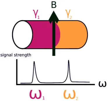
characteristic of the atom and the molecule in which the atom resides. (see Figure1.1). The Fourier transform of the NMR signal, called the NMR spectrum, can have one or
more peaks. A peak at frequencyωindicates that a species of nucleus with gyromagnetic ratio ω/B0 is present in the sample. Measuring the applied magnetic field yields the
gyromagnetic ratio for each peak. Since each species of nucleus has a known ratio, the
composition of the sample may be deduced (see Figure 1.2).
The shape, duration, and number of magnetic pulses applied to the sample is a broad
topic with many applications. [4] [1] Here narrow our attention to a simple type of NMR spectroscopy, the Free Induction Decay experiment.
1.2
Free Induction Decay
When the transverse magnetic field is turned off, the magnetization continues to precess
around the z-axis, under the effect of the magnetic field B0, at the Larmor frequency. The precession does not last forever but it will decay with a time constant called the
transverse relaxation time T2. [4] The detected decaying signal is called Free Induction Decay (FID).
A primary consideration of an NMR experiment is to excite the spins of the nuclei so
Background 4
Figure 1.2: A visualization of basic NMR spectroscopy. If the differently colored regions represent regions of nuclei with different gyromagnetic ratios, then the two
materials may be distinguished in the Fourier spectrum via Equation1.1.
at the resonant frequency ωL. The signal strength also depends on the magnetization
angle θ, which is increased by increasing the magnitude and duration of the additional field Bc. The maximum signal is achieved when θ = π/2, when the magnetization is
entirely within thex-yplane, orthogonal toB0. As a result, it is possible toover-excite the spins by pulsing for too long or by using a too strong magnetic fieldBc. For dipoles
in this state, any further excitation will extend the angle beyondθ=π/2 and the signal
will begin to diminish.
The duration of data collection is also an important consideration in NMR. Collecting
more data increases the resolution of the signal in the frequency domain at the expense
of increasing spectrum noise. As a result, it is best to stop collecting data when the the
signal reaches noise level. Any additional data collected will add more noise than signal
to the Fourier spectrum.
At the same time, longer data collection times result in higher resolution in the spectral
domain, according to the Nyquist theorem, [7] making longer collection times desir-able when possible. As a result, reduction in the signal-to-noise ratio (SNR) allows for
higher resolution data. A higher resolution means that closely-spaced peaks can be easily
distinguished, leading to more precise spectroscopic measurements and better
discrimi-nation of nuclear species. However, even a high-resolution spectrum may be muddled by
Background 5
boundaries between the two may overlap and the distinction may disappear.
Further-more, wide peaks are typically associated with low SNR. Small linewidths are especially
important for a more sophisticated measurement achievable through free-induction
de-cay - a one-dimensional spin density image.
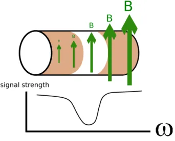
While NMR spectroscopy can distinguish between different species of nuclei, it can also
be used to spatially locate the spins, when used in conjunction with a magnetic field
gradient. In the former case, the observed frequencies may vary because of different
gyromagnetic ratios or chemical composition of the sample. In the latter case, however,
frequencies vary because of an inhomogeneous magnetic field B0. By applying a dif-ferent magnetic field to difdif-ferent regions of a sample, the frequencies of precession will
correspondingly vary, assigning a frequency to each location along the magnetic field
gradient (see Figure 1.3). By applying a magnetic field gradient applied along the x -direction, for example, will spatially label the spin along that direction. In the frequency
domain, the signal will be nothing else than the projection of the sample spin density
along the direction of the applied gradient. In the one-dimensional case, the extraction
of an image is remarkably simple.
Figure 1.3: A visualization of one-dimensional imaging with NMR. If the colored
region represents the presence of a substance with resonant nuclei, then the empty region in the center will not produce a signal. The variable magnetic field will then
generate a gap in the spectrum at the corresponding Larmor frequency.
The strength of the signal is proportional to the concentration of nuclei in the sample.
Regions of the sample with fewer precessing nuclei will generate a weaker signal, resulting
in a dip in the spectrum. Similarly, an excess of precessing nuclei creates a peak in the
spectrum. In other words, the shape of the signal in frequency space is a reflection of the
sample spin density along the direction of the magnetic field gradient. If the frequency
Background 6
characteristic of the nuclei in different molecules, then the technique becomes a way to
spatially resolve the chemical composition of a sample.
The manifestations of NMR techniques take many forms. The next section introduces
a subset of NMR experiments that is the topic of this dissertation.
1.3
Earth’s Field NMR
Nuclear magnetic resonance spectroscopy is typically performed by using strong
elec-tromagnets which make the resulting signal easier to detect. For magnetic fields on the
order of Tesla, the Larmor frequency is in the radio frequency range. These equipments
are expensive and motivated the search for cheaper alternatives. The Earth naturally
provides a magnetic field which is only about 50 µT but can be used in the place of
artificial magnetic fields. The ubiquity and uniformity of this field makes Earth field
nuclear magnetic resonance (EFNMR) a suitable solution for low-field spectroscopy.
Environmental study is an important motivation for EFNMR spectroscopy. [8]. Because the equipment involved lacks large electromagnets, the electronics can be powered by
portable batteries. Portability is a major advantage of the design. Furthermore, while
the Earth’s magnetic field is weak, resulting in smaller magnetization (see Equation1.1), the field is generally quite homogeneous. The importance of this homogeneity stems from
the fact that dipole precession occurs everywhere in the sample, and the full volume of the
sample contributes to the FID signal. If the Earth’s field is inhomogeneous throughout
the sample, the Larmor frequency also would be non-uniform, causing a frequency spread
in the spectral domain. Because the Earth’s field is very homogeneous, a very narrow
peak can be generated.
One way to overcome the inherently weaker FID signal in EFNMR is by pre-polarizing
the sample prior to the measurement. When a sample is removed from a magnetic
field, its magnetization does not immediately disappear. Instead, the excess of aligned
dipoles N↑−N↓ decays with a time constant T1, the longitudinal relaxation time. [4]. The magnetization vector will align with any external field, whether the external field
generated the magnetization or not. To augment the magnetization of a sample while
still using Earth’s field, the sample can be placed in a strong magnetic field, where it
acquires a larger magnetization. Then the sample is rapidly placed in the more
homo-geneous Earth’s magnetic field before the magnetization returns to thermal equilibrium
value. Using this method, the advantages of a strong signal and homogeneous field are
Background 7
1.4
Applications
The advantages of portable EFNMR are ideal for certain environmental research
ap-plications because in situ analysis is often a great asset. An example application was
provided by Callaghan et al. in Antarctic sea ice. [8]. EFNMR spectroscopy was used to investigate the structure and distribution of brine pockets in sea ice, to better
under-stand the ice’s physical properties for use in climate modeling. Ice cores were collected
on-site, but transport to a lab away was not possible because the changing temperatures
and humidities during transport would damage the samples. The harsh conditions of
the site made traditional NMR impractical. Instead, an EFNMR spectrometer, similar
to the design presented here, was used to test samples soon after extraction. In their
1990 article, Stepisnik et. al. cite the lower cost of EFNMR as motivation for their
two-dimensional imager. [9]
1.5
Objective
This dissertation aims to realize a low-cost EFNMR spectrometer based on a design
provided by Michal [10]. Michal’s work attempted to provide a means for small labs, students, and amateurs to access NMR spectroscopy. In this work, we investigate the
advantages and possible pitfalls of the design by conducting free-induction decay
exper-iments on water samples. We also evaluate the potential of the design as a platform for
one-dimensional imaging, using a gradient coil to generate the inhomogeneous magnetic
Chapter 2
Circuit Design
2.1
General Approach
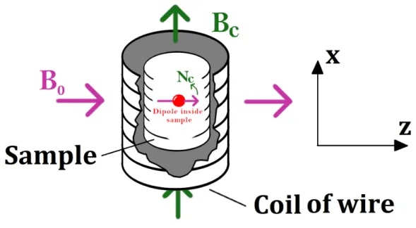
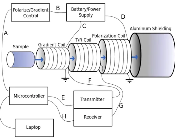
Figure 2.1: Schematic layout of experiment.
The purpose of the EFNMR spectrometer is to measure free-induction decay signals from
precessing magnetic dipoles in a sample and extract their Larmor frequency. Therefore,
a coil is needed to induce an oscillating magnetic field in the sample. In addition, a
Circuit Design 9
coil is needed around the sample to detect the dipole precession. In fact, the same coil
can accomplish both tasks. A laptop computer powers a microcontroller and uploads
the programs to control the experiment (see Figure 2.1). The microcontroller actives a power supply control circuit (A) which supplies current to the polarization coil (B) and gradient coil (C). After a time larger than T1, the polarization coil is turned off adiabatically to allow the sample’s magnetization to align along the Earth’s magnetic
field. Then the microcontroller initiates the oscillating field Bc (D), generated with
the transmitter, which enters the T/R coil (F), rotating the nuclear spin magnetization by an angle θ. The free precession of the transverse magnetization around the Earth
magnetic field induces a voltage in the T/R coil. The receiver opens and detects the
signal (G) before relaying the data to the microcontroller (H).
The oscillating magnetic field Bc is generated by passing an oscillating current at the
desired frequency through the coil. This oscillating current is supplied with the
trans-mitter, which ensures the magnetic perturbation successfully causes dipole precession.
The receiver amplification is necessary to boost the detected signal to a strength that
the microcontroller’s ADC (analog-digital converter) can detect. These considerations
and those of filtering are discussed in theReceiversection.
The key components of the EFNMR spectrometer are:
transmit/receive (T/R) coil - needed to induce an oscillating magnetic field Bc
transverse to the main magnetic field B0, and to detect the precession of the transverse magnetization around the main magnetic fieldB0
transmitter - made up of a microcontroller and an amplifying/filtering circuit, needed to supply theBc field
receiver - uses the microcontroller and a separate amplification/filtering circuit, needed for receiving and filtering of the dipole precession signal from coil
microcontroller - Arduino Uno or Mega programmed with open-source software, available athttp://www.phas.ubc.ca/~michal/Earthsfield, controls operation of
ex-periment
sample - water bottle placed into T/R coil
laptop - used to store the collected data and interfaces with the microcontroller via USB cable
Circuit Design 10
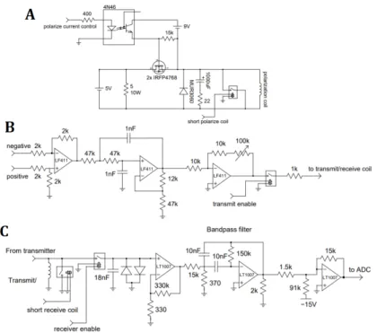
Figure 2.2: Schematics for the transmitter, receiver, and polarization control circuit.
Adapted from Michal [10].
polarization coil - large coil placed on the outside of the T/R coil to generate a large, temporary magnetic field that polarizes the spins
Not shown in Figure2.1 is the magnetic probe, used to measureB0 for calculating ωL.
Most modern cell phones contain a probe that indicates the strength and direction of
magnetic fields with reasonable accuracy.
We base our design for the circuit on the design provided by Michal [10]. The schematics of the transmitter, receiver, and polarization control circuit are shown in Figure2.2. The gradient control circuit, not provided by Michal, is very simple. It consists of a reed
relay that connects a battery to the gradient coil when activated by the microcontroller
(see 3.5).
2.2
Microcontroller
For our simple FID experiment - i.e. excitation of the magnetization and acquisition of
the FID - the software configures the Arduino to output two digital waveforms at the
necessary frequency, phase, and duty cycle for the transmitter to combine them into
a zero-centered sinusoidal pulse. The software programs digital signals to be sent to
Circuit Design 11
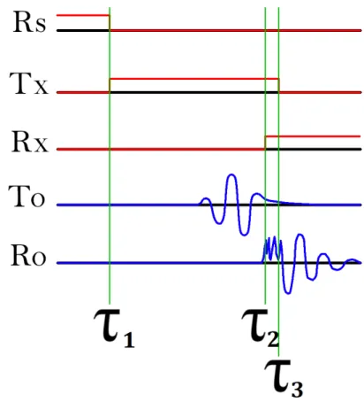
Figure 2.3: Timing diagram for the communication between the microcontroller and T/R circuit. First, at aboutτ1, the receive short (Rs) signal deactivates, which
discon-nects the coil from ground (which otherwise prevents the coil from acquiring a floating voltage). Simultaneously, the transmit connect (Tx) signal connects the transmitter to the coil. At some later time, the signal is transmitted, as seen in the transmitter out-put (To). When the receiver is activated by the receiver connect (Rx), a signal passes through the output of the receiver (Ro). The duration of the signal is controlled by the microcontroller’s software. The difference between τ1 and τ2 is about 60 ms, whereas
betweenτ2 andτ3only about 2 ms elapse.
the Arduino is used to capture data from the output of the receiver. The software then
allows the data to be visualized and stored.
2.3
Transmitter
The transmitter must convert a digital (pulse-width modulated) waveform from the
mi-crocontroller to a sinusoidal waveform of a short duration with no DC offset. To achieve
the resonant condition, and effectively rotate the magnetization onto the transverse
plane, the frequency of this waveform must be equal toωL. The microcontroller outputs
a typical digital voltage of 0 or 5V. To create a zero-centered pulse, we follow the design
provided by Michal. First two digital signals, exactly out of phase, with duty cycle of
about 0.4, are passed into a summing amplifier, with one of the signals connected to the
Circuit Design 12
After this stage, the transmitted signal is smoothed into a sinusoid with a low-pass
filter. A final stage carries out further amplification, with adjustable gain provided by
adding a potentiometer as a feedback resistor. We label the final voltage amplitude of
the transmitted waveform VT. Varying the strength of the transmitter output changes
the strength of the field Bc and the angle of rotation of the magnetization away from
thez-axis. Increasing theVT has a similar effect to increasing theBc duration.
2.4
Receiver
The receiver carries the task of amplifying the tiny NMR signal from the T/R coil.
Amplification is necessary to bring the strength of the signal within the dynamic range
of the analog-digial converter (ADC). It also performs a bandpass filtering stage to
process the signal before conversion into digital data by the microcontroller. The last
stage of the receiver performs some amplification, but more importantly it includes a
“pull-up” resistor that increases the center voltage of the signal from zero to about 2.5
volts. This is necessary because the microcontroller has an ADC that only reads from
zero to 5 volts. In other words, the “bottom half” of the signal would be lost without
this final stage.
The bandpass filter must be tuned to the signal frequency ωL. For protons in water,
the gyromagnetic ratio is 42.6 MHz/Tesla, corresponding to 2130 Hz for a typical Earth
field strength (50 µT). The receiver places the T/R coil in series with an inductor to create a resonant LCR circuit that amplifies signals within a given frequency range. The
resonant frequency in terms of the T/R coil inductance L and the capacitor valueC is
ω0 = 1 √
LC (2.1)
Chapter 3
Development and Experiment
Although the schematic design from Michal [10] details the theoretical function of the electronics, a practical spectrometer requires careful consideration regarding the
place-ment and maintenance of components. In this chapter, we outline the prototyping
process that led to a functional spectrometer and demonstrate how experiments were
conducted.
3.1
In-Lab Board Manufacturing
The costs and wait time associated with ordering printed circuit boards from a
manu-facturer prompted an attempt to print a prototype board in the lab.
A circuit design was drawn using the ExpressPCB software and the photo editor GIMP.
This black-and-white photo (see Figure 3.1) was printed onto magazine paper. The ink was transferred to a copper-coated silicon board by pressing the paper onto the
copper with a hot iron after soaking the paper in water. Then the ink-imprinted boards
were placed into a ferric acid solution for 10 to 20 minutes, until all the exposed, ink-free
copper dissolved away, leaving only the printed design. The result is a functional printed
circuit board, as shown in Figure 3.2.
Important notes from the printing process include:
Large pads for solder joints are essential since all of the parts must be surface-mounted.
The ink from the magazine paper does not always cleanly adhere to the copper surface - it is often necessary to fill in missing sections of ink with a permanent
marker.
Development and Experiment 14
Figure 3.1: The design for the lab-manufactured board. Note the four separate segments, which allow the design to printed on smaller silicon pieces.
Figure 3.2: A segment of the second prototype after the copper was etched in an acid
bath.
The design in Figure3.1 was made to closely resemble an already-existing breadboard prototype that was known to work, with good stability characteristics (that is, the
gain could be set relatively high without causing feedback oscillations). Since unwanted
feedback oscillations, analyzed in Chapter 4, depend sensitively on the placement of
wires and components, it was expected that a similar board design would have similar
stability characteristics.
After installing components and connecting batteries and the Arduino microcontroller,
the spectrometer took the form shown in Figure 3.3. This device was connected to a shielded T/R coil, surrounded by a polarization coil and various metal objects
care-fully located to improve the Earth’s magnetic field homogeneity in the inhomogeneous
environment of the laboratory.
Development and Experiment 15
Figure 3.3: The lab-printed circuit board (assembled from four individual segments)
with a connected Arduino Uno.
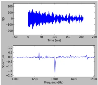
Figure 3.4: Well-shimmed result of FID experiment using Prototype II obtained inside
the laboratory.
feedback oscillations start to occur. For the lab printed board, this first stage gain
is about 270. This is smaller than the 1000-fold gain reported in Michal [10], or the 450-fold gain in the breadboard circuit. However, the gain is still high enough for easy
detection of the NMR signal, as shown in Figure3.4.
Unfortunately, the densely-packed surface mount components are especially difficult to
remove and replace. Faulty op amps and relays, among other issues, are a common
roadblock when using the spectrometer, so the difficulty of repair makes long-term use
Development and Experiment 16
Figure 3.5: The polarizer (top) and gradient (bottom) circuits.
Figure 3.6: An image of the professionally-manufactured PCB design in EasyEDA.
Red traces appear on the top layer and blue traces on the bottom layer.
The circuits controlling the polarizing coils and gradient coils were constructed using
breadboards, since the design is relatively simple and easy to replicate. The breadboards
Development and Experiment 17
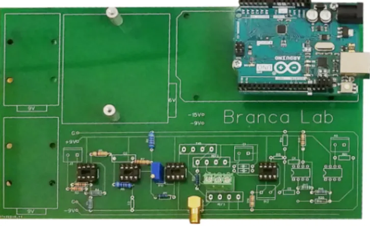
Figure 3.7: The professionally-manufactured PCB, with some components installed.
To minimize material damage to connecting wires, the Arduino and batteries (not shown) can be screwed securely onto the board. The PCB can hold either an Arduino
Uno or Mega.
3.2
Professionally-Printed Board
To ensure the long-term durability and reliability of the spectrometer, a second prototype
was built with a professionally-printed board (see Figure 3.6and 3.7). Because battery packs were connected to the first PCB with loose wires, and not secured in place, frequent
use of the board caused the wires to bend and eventually break. The second prototype
has space to mount the batteries and Arduino on the same board as the transmitter
and receiver. Other common stress points of the previous design, including the SMA
connector, potentiometer, tuning capacitor socket, and others were all secured more
firmly in the second PCB.
3.3
Calibration of Bc Frequency and Duration
To test the spectrometer, a simple experimental procedure was followed. Inside the
laboratory, the field strength was measured with the magnetic probe to be 30 µT with
limited precision (uncertainty ± 2 µT). As a result, the resonant frequency ωL was
known with an uncertainty of ± 200 Hz. Detection of a signal at ωL was possible as
long as the frequency of Bc was close enough to the resonant frequencyωL.
Data was collected and visualized to look for signs of a promising FID spectrum. For
each test run, an additional period of data collection occurred with the polarizer turned
off. This control test identified which peaks in the spectrum were due to noise and
Development and Experiment 18
trial but not the control, we were able to refine the estimation of B0 and the supplied frequency of Bc.
The ideal transmitter strength was also not known, soBcduration was varied in addition
to frequency. Inside the laboratory, a waveform duration of 6 half-cycles (with VT = 1
V) consistently yielded a strong signal, so most experiments were conducted with this
setting. The exception was an outdoor experiment described in the Variation of Bc
Duration section.
3.4
Shimming of Earth’s Field and Gradient Coil Tests
In the free-induction decay experiment, the quality of the spectrometer data is partially
determined by the linewidth of the peak in the signal spectrum. This linewidth is
dependent on the homogeneity of the external magnetic field. Any spatial variation
in the magnetic field will cause dipoles in different regions of the sample to precess at
different rates, creating a range of frequencies rather than a uniform response.
Although the Earth’s magnetic field provides a very homogeneous magnetic field in
the absence of human activity, indoor locations such as laboratories typically have large
spatial variations in the ambient field. To make laboratory Earth-field experiments
prac-tical, one can introduce additional disturbances to the magnetic field to cancel out the
variation already present. In NMR, the practice of adding small magnetic fields to even
out B0 is known as shimming. There are two principal types of shimming: active and
passive. Active shimming uses an electromagnet or ferromagnetic objects that generate
a magnetic field regardless of its surroundings. Passive shimming uses paramagnetic or
diamagnetic objects that respond to existing magnetic fields by generating small fields
of their own. Passive shimming is typically very simple but makes a smaller impact on
the inhomogeneities.
In the laboratory setup, we place several metal objects (screwdrivers and an aerosol can)
near the coils for passive shimming. Finding the optimal configuration of objects is a
case of trial-and-error. See Figure 3.8.
We also implemented an active shim using the gradient coil. The gradient coil creates
a magnetic field that varies approximately linearly along the x direction. The results of the active shimming experiment are included in the Active Shimming section. This
experiment also served as validation for the gradient coil functionality. For active
shim-ming, the current through the gradient coils is adjusted to be very low, less than 0.1 mA.
To operate the one-dimensional imager, we use larger currents, widening the spectral
Development and Experiment 19
Figure 3.8: Aerosol can and screwdrivers used for passive shimming.
3.5
Change in Inductance from Shielding
To reduce the interference of ambient electrical signals with the T/R coil, a segment
of large aluminum tubing is used as shielding. This shield contains not only T/R coil,
but also the gradient and polarization coils. Note that the introduction of the shielding
changes the inductance of the coil. As the coil generates an oscillating magnetic field,
electric currents are induced in the conductive shielding, which in turn generate their
own magnetic fields that may be picked up by the receiver. When tuning the circuit, it
is important to recheck the inductance of the coil with the shielding in place.
The ability of the shielding to reduce ambient noise is significant and clearly visible in
Figures3.9.
3.6
Pre-Polarization of Nuclear Spins
Although the polarization coil is a simple and reliable way to polarize the spins, it
does add complexity to the design that may make initial debugging more difficult. To
simplify the prototyping processes, we use a large permanent magnet as a temporary
spin polarizer. The device consists of two neodymium rare-earth magnets attached to
two metal walls spaced about 10 cm apart. The magnetic field strength in the region
between the two magnets is about 0.2 Tesla. The water sample polarizes in about
Development and Experiment 20
Figure 3.9: Top: typical test run, with a shielded T/R coil. Bottom: same experiment
as top, but without the shielding in place.
magnet for 20 seconds. Then it is quickly removed from the magnets and placed into
the T/R coil before the polarization wears off.
3.7
Compatibility of Arduino Uno and Arduino Mega
Michal’s design calls for an Arduino Duemilanove microcontroller. We use the very
similar Arduino Uno for the spectrometer and experience no compatibility issues. Since
the Arduino Uno’s limited memory can pose a significant restraint on the complexity of
modifications to the default code, we tested the compatibility of a larger cousin of the
Uno, the Arduino Mega. A slight modification must be made to the code location
sbi ( PRR , P R T W I );
sbi ( PRR , P R S P I c );
in the script “ArduinoCode”. HerePRR refers to the Power Reduction Register - the Uno has only one, but the Mega has two. Therefore, replacing the above code with
sbi ( PRR0 , P R T W I );
sbi ( PRR0 , P R S P I c );
sbi ( PRR1 , P R T W I );
Development and Experiment 21
activates the power reduction command on the Mega. This is the only compatibility
issue. We successfully used a version of the code, larger than the maximum program
size of the Uno, with the Arduino Mega.
3.8
Outdoor Experiments
After initial experiments in the laboratory, field experiments were conducted in Battle
Park, a forest located near the UNC campus. The park contains large patches of
unde-veloped land hundreds of meters from power lines, buildings, or vehicles. The absence of
overhead power lines is a particularly important criterion for choosing an EFNMR
exper-iment location. Figure3.10shows the time-domain signal of a control experiment (with no sample) conducted about 30 meters from a typical medium-voltage power line. The
sensitive PCB electronics picked up many frequencies from the large AC current in the
power line, leading to a large output signal that somewhat resembles a real FID signal.
The significance of the power line interference demonstrates that an ideal experimental
location will be at least several hundred meters from power lines.
A photograph of an FID experiment conducted in the forest is provided in Figure3.11. The coordinates of the experiment location are 39.914028 N and 79.042140 W.
To conduct the outdoor experiment, a portable power supply is required for the
polar-ization coil. We use a 6V lead-acid battery attached in place of the wall power supply.
For manual polarization we also bring the neodymium magnet to the experiment site.
3.9
Active Shimming
Under conditions where feedback oscillations do not affect the signal acquisition, we
measure the effect of small gradient fields on the NMR linewidth. Since the frequency
resolution of the spectra is low, we cannot directly obtain the linewidths. Instead,
we assume that the signal strength S (defined in Equation 3.1) is the same in each measurement. This assumption follows from the fact that the transmitted field Bc
is kept at constant strength and duration, and the polarization strength is also held
constant. Based on Equation 3.1, if the width of the signal increases but S remains the same, the average value of the signal spectrum ˆF(ω) decreases. We assume each spectral peak has approximately the same shape, so that the average value of the peak
is proportional to its maximum value. Therefore, we record for the maximum value
in the spectrum as a proxy for linewidth. Higher maximum value indicates narrower
Development and Experiment 22
Figure 3.10: Time-domain (top) and spectral-domain (bottom) data from a control experiment with a large spurious signal generated from nearby power lines.
these experiments, different resistors were used to change the current in the gradient
coil. For each resistor, the resulting spectral maximum was measured and plotted as
a function of the inverse of the resistance, which is proportional to the current and
therefore a proxy for the strength of the gradient magnetic field.
3.10
Linewidth
The limited resolution of the collected spectral data prevents a precise measurement
of the linewidths, but we can place bounds on linewidth to compare the NMR signal
characteristics under outdoor and indoor conditions. We refer to the spectral resolution
Development and Experiment 23
Figure 3.11: Outdoor experimental setup. In this example, the permanent magnet is used to polarize the sample. Note that the polarizer magnet must be kept several meters from the coils to prevent interference with the Earth’s magnetic field at the
location of the coils.
Figure 3.12: The relation of maximum spectral value with relative gradient magnetic
Development and Experiment 24
Figure 3.13: A closeup of the spectra for several measurements taken with differentBc
durations or half-cycles (HC). The integration range for the signal strength calculation is shown by the two black lines (from 2122.5 Hz to 2125.5 Hz).
counting the number of spectral support pointsNω in the peak located above one-half
of the maximal value. The upper bound on linewidth is ∆ω(Nω + 1), and the lower
bound is ∆ω(Nω −1). Using this method, we calculate that the narrowest linewidth
achieved inside the laboratory is 16 ± 8 Hz. Because the smallest Nω for the spectra
collected outside is 1, we cannot define a lower bound. We report that the linewidth is
less than 0.96 Hz.
3.11
Variation of Bc Duration
To check that the Bc duration was optimized for maximum signal strength, we varied
the Bc duration, measured by integer number of half-cycles. In this experiment it was
valuable to maximize SNR so the variation of signal strength was most apparent and
least affected by noise. In this case the optimal setup was the outdoor experiment with
manual polarization, which demonstrated the largest and sharpest spectral peaks.
To calculate the signal strength we determine a range of frequencies spanning the width
at the base of the peak (see Figure 3.13). Because the spectral signal ˆF(ω) is present across a small range of frequencies, we define the signal strengthS to be a sum of each frequency’s contribution
S = Z ωb
ωa
ˆ
F(ω)dω (3.1)
Development and Experiment 25
Figure 3.14: Variation of signal strength with Bc duration, measured outside.
We display the observed variation in Figure3.14. We note a maximum response at 8 half-cycles, and record a significantly stronger signal whenever the number of half-cycles is
even (i.e., theBcduration is an integer multiple of the period 1/ωL). All measurements
Chapter 4
Hardware Performance
Throughout the course of experiments, both PCBs were plagued with feedback
oscil-lations. The feedback oscillations are characterized by a large signal greater than the
maximum voltages that the op amps can supply and a frequency equal to that of the
bandpass filter frequency. The term “feedback oscillation” refers to the fact that they
typically occur when the gain of the receiver is set too high, as if some feedback
mech-anism causes the highly sensitive output of the amplifiers to couple back into the input
and become unstable. The oscillations completely erase any readable signal and persist
even after the signal has finished.
Some observed features of the feedback oscillations make it difficult to explain what the
coupling mechanism is. In the following section, we outline experiments and tests that
helped to characterize the nature of the feedback oscillations.
4.1
Hysteresis
Hysteresis is the property of a physical system to behave according to rules based on
past states, not just the current state. The feedback oscillations exhibit hysteresis with
respect to the variable gain on the first amplification stage. To demonstrate this, we
replace the 330 kOhm resistor with a potentiometer. We feed a continuous small signal
from a function generator into the receiver. Increasing the potentiometer from a small
value P, and thus increasing the gain, we first observe feedback oscillations begin at
P =P0. Then we decrease the potentiometer value belowP0, and the oscillations persist. Only after we lower the potentiometer to some other value P1 do the oscillations cease
(see Figure4.1).
Hardware Performance 27
Figure 4.1: A qualitative sketch of the relationship between gain and feedback
os-cillations. Gain must be reduced to much lower than the unstable threshold to return the receiver to a normal state. In effect, there are two different thresholds: a “rising threshold”, the point at which an increasing gain initiates the oscillation, and a “falling threshold”, the point at which a decreasing gain no longer supports the oscillation. The
rising threshold exceeds the falling by a factor of about 3.
Figure 4.2: This oscilloscope data shows the onset of a feedback oscillation, just as
Hardware Performance 28
4.2
Effect of PCB Design on Feedback Oscillations
The professionally-printed circuit board fared much worse with respect to feedback
os-cillations than the lab-printed board. The typical max-gain-before-oscillation of the lab
PCB is about 14000, but only 2200 for the professional board. In the latter case with
this small gain the SNR becomes too low and NMR spectroscopy is no longer practical.
The two boards were designed to have nearly indentical component layouts and similar
wire paths (see Figures3.1and3.6). The primary difference between the two is that the power for the pull-up resistor (two AA batteries) are connected via a wire that runs
un-derneath the second stage of the receiver amplifier (as opposed to away from the board
entirely). This design choice aimed to keep the board compact and reduce the number of
jumper wires dangling above sensitive components. However, it may have had a serious
negative effect on the stability of the professional board.
Another significant difference in the two boards is the placement of ground wires. Both
boards have two common ground wires that run above and below the components in a
straight line. On the lab board, these ground wires are only connected by a wire on the
receiver end of the PCB. On the professional board, the ground lines are connected on
both ends.
4.3
Effect of Ground Wire Placement
The redundant connection to ground may seem innocuous, but tests with a breadboard
version suggest it may be an important factor for causing oscillations. Placing the ground
connection wire on the receiver side, as in the lab board, always results in feedback
oscillations. On the other hand, placing the wire only on the transmitter side does not
cause oscillations. This observation appears to contradict that of the previous section
if induced voltages on ground wire connectors are to blame for feedback oscillations.
However, the fact that the feedback effect can be controlled with the placement of a
seemingly trivial connection points to a coupling effect involving the ground wire.
Another effect relating to the ground wire complicates matters further. On the
bread-board spectrometer, if the ground connection to the Arduino is connected to the upper
ground rail, no oscillations appear. Oscillations always appear if the ground link to the
Hardware Performance 29
4.4
Effect of Analog Input Connections on Feedback
Os-cillations
Regardless of the board, whenever feedback oscillations do occur, they can be observed
by connecting the output of the receiver to an oscilloscope. An interesting phenomenon
occurs when the receiver output remains connected to the oscilloscope but is
discon-nected from the microcontroller analog input. This input contains an analog-digital
converter that sends voltage data to a computer. Disconnecting this wire prevents the
data from being saved. However, it also prevents feedback oscillations. The oscilloscope
displays signals that would have been lost otherwise. In fact, the professional PCB is
capable of producing high quality NMR signals, as long as it is not sending the signal
to the microcontroller. Interestingly, the oscilloscope functions much the same way, in
principle, as the microcontroller analog input - it takes in a physical voltage from a wire
and generates a digital representation of the voltage value. If the oscilloscope were not
so expensive, it could easy replace the Arduino as the data acquisition hub for this
spec-trometer design. Since the precise input impedance, sample rate, etc. of the Arduino
and oscilloscope are not known, we cannot compare the two devices to determine the
cause of the discrepancy. Furthermore, the problem is not unique to a particular
Ar-duino - we tested several units including genuine and imitation versions of the ArAr-duino
Uno and Mega.
4.5
Test with Unity-Gain Amplifier on Analog Input
One proposed explanation for the behavior of some PCBs when connected to the analog
input is that the Arduino input has a low input impedance compared to the oscilloscope.
If this were true, the Arduino would draw more current from the output of the receiver.
This current then might inductively couple to other parts of the circuit. To test this,
we install a unity-gain op amp circuit on the output of the receiver. We place the
op amp several inches away from the receiver and connect the amplifier output to the
Arduino. We expect that if inductive coupling on the receiver output causes feedback
oscillations, the op amp will prevent them because the input resistance is so high. This
way, the current leading away from the PCB is negligible and the Arduino still receives
the signal. However, this configuration still yielded feedback oscillations. Surprisingly,
the unity gain non-inverting op amp configuration caused oscillations even without being
connected to the Arduino. This suggests that the effect of the non-inverting op amp
on the circuit is similar to that of the Arduino. The significant difference between
Hardware Performance 30
a connection from the output to ground via a resistor. It is possible that non-zero
resistance in the ground wire causes the ground voltage in different parts of the circuit
to be slightly different, leading to some electrical feedback effect.
4.6
Test with Second Microcontroller
Since the goal of the device is low-cost spectroscopy, we attempt to use another Arduino
for the sole purpose of reading voltages in the hopes that the feedback mechanism would
decouple. To do this, we write Arduino code that stores voltage data when triggered by
another Arduino. This allows one Arduino to control the operation of the experiment
while the other stored FID data. However, in order for this configuration to work, the
ground voltage of both Arduinos needs to be the same. Otherwise, floating voltage offset
will make the output of the receiver unreadable to the 0 to 5 volt analog pin. However,
anytime the grounds of the two microcontrollers are connected and the output of the
receiver is connected to either Arduino, feedback oscillations result. This is true whether
the microcontrollers are connected to the same laptop or to two different ones.
4.7
Initiation Timing of Feedback Oscillations
Critical to the understanding of the feedback oscillations is the initiation timing. Since
different control signals occur at different times, observing the beginning of a
feed-back oscillation may pinpoint the source. Observing the output of the receiver with an
oscilloscope, we see that the oscillations begin at timeτ1(referring to Figure2.3), corre-sponding to the receive short command where the T/R coil is grounded. However, if we
unplug the wire delivering that command, feedback oscillations are initiated anyway at
timeτ2, when the receiver opens. This suggests that any sudden shift in voltage triggers the oscillations. In normal experiments, we observe a characteristic “ring-down” of the
T/R coil as the receiver opens. The signal on the output during this ring-down phase
often reaches the power rails.
4.8
Other Observations
The likelihood of feedback oscillations seems to be also location-dependent. The same board with the same parameters can exhibit oscillations one day and not the
next. While performing experiments outside, the gain usually had to be lowered
Hardware Performance 31
culprit, since the induced voltage increases proportionally to the frequency, and
the ambient magnetic field outside required twice the Bc frequency as the field
inside the lab.
We can connect the analog input of the microcontroller to various stages of the circuit, not just the final one. Connecting the output of the second amplification
stage results in feedback oscillations only triggered by the opening of the receiver
(not the receive short command) and they disappear when the receiver is closed,
unlike the normal oscillations. Connecting to the output of the first stage gives no
oscillations, and the input of the first state looks just like the output of the second
Chapter 5
Parasitic Inductance Analysis
From Maxwell’s equations, we can formulate a model for the unwanted electromagnetic
coupling between different parts of circuit boards. Specifically, as the NMR signal drives
a small AC current through the components of the PCB, oscillating magnetic fields are
created. These fields can induce unwanted voltages in nearby components. Although for
low-frequency applications these “parasitic inductance” effects do not generate
appre-ciable voltages, the large gain of the receiver amplifiers make them extremely sensitive
to coupling effects.
In this analysis we create a two-dimensional model of the receiver on the lab-printed
circuit board that captures most of the conductive elements. Using a numerical
integra-tion technique, we find the coupling strength between each component and wire trace
on the PCB. We use the coupling model to identify problematic areas or components
that generate or amplify unwanted induced voltages. Although the model is crude and
not designed for quantitative determination of maximum possible gain, for example, it
does inform certain guidelines and strategies to mitigate parasitic inductance.
5.1
Theoretical Framework
We start with the equation known as Faraday’s Law [11]
∇ ×E=−∂B
∂t (5.1)
and the equation known as Ampere’s Law
∇ ×B=µ0
J+0
∂E
∂t
(5.2)
Parasitic Inductance Analysis 33
We opt to neglect the second term on the right side of Ampere’s Law. The reason
for this choice is that this term represents a coupling between in electric and magnetic
fields that gives rise to electromagnetic radiation. In electronics for conventional NMR,
EM radiation is a major source of noise generation and a key focus of electromagnetic
interference (EMI) analysis. [12] However, the energy radiated away by EM waves is inversely proportional to the square of the signal frequency. [11] As the frequency of the signals generated in our circuit is only 1-2 kHz, the time derivative of the electric field
is small. In other words, we do not analyze “antenna-like” behavior of the components,
but only mutual inductance effects.
We take the curl of Equations5.1 and 5.2to see that
∇ ×(∇ ×E) =−∂(∇ ×B)
∂t =−µ0 ∂J
∂t (5.3)
We can use the curl-curl vector identity [11],∇ ×(∇ ×E) =∇(∇ ·E)− ∇2E, to simplify. We are not interested in buildup of electric charge, so by Gauss’ Law, the divergence
∇ ·E is zero. The problem turns into three separate Poisson equations.
∇2E=µ0
∂J
∂t (5.4)
where∇2 is the vector Laplacian operator. From this equation, we can see that induced
electric fields are always parallel to the change in current.
In this analysis, we consider all components to be contained in a two-dimensional x-y
plane, which simplifies the calculations greatly. Since no current flows in the z direc-tion, the electric field has no z-component as well. We note that the two-dimensional assumption neglects the three-dimensional shape of capacitors, jumper wires, and other
components that extend above the surface of the PCB. Also neglected are the inductive
effects of the operational amplifiers, relays, and terminal blocks.
After solving Equation5.4, one can find the induced voltage in an electronic component with the following integral
ε=− I
C
E·dl (5.5)
whereC is some curve in thex-y plane. In our analysisCalways follows paths represent-ing wires on the PCB. Combinrepresent-ing Equations5.4and5.5, we can, in principle, determine the induced voltageεon a wire defined byCdue to an arbitrary changing current density
Parasitic Inductance Analysis 34
5.2
Numerical Implementation
We divide the simulated PCB into a grid of discrete points with separationdx. All of the
wires point along either thexdirection or theydirection, so the induced electric field is also either pointing along ˆior ˆj, never diagonal. This has an important consequence: a
varying current pointing in thex direction cannot induce a voltage in ay-pointing wire, as Equation 5.4is made from three fully independent equations.
Suppose that we have two wire elements A and B broken intoi and j number of cubes of side length dx (refer to Figure 5.1). Let us refer to the position of cube Ai as ri
and of cube Bj as r0j. Wire A carries a current density J. The desired quantity is the
electric fieldEj at pointr0j due toJi at pointri. We approximate the cube Ai as a point
current source. Then the solution to the Poisson equation has well-known form (based
on Gauss’ Law) [11]
Ei =
µ0 4π|r−r0|
Z
V
∂tJidV (5.6)
where V is a volume. Since ∂tJi is constant within the discretize cube, the integral is
just∂tJidx3, or∂tIidx.
We note that the Laplacian is a linear operator. That is, the electric field caused by the
sum of many current elements is the same as the sum of many electric fields caused by
single current elements. Thus, we can sum the electric fields caused by each Ai to get
the total field on Bj induced by A.
The next step is to calculate the voltage along the entirety of B. We can discretize
Equation 5.5to get
εB =−
X
j
Ejdx (5.7)
We can now define the coupling constant MAB as the voltage induced on wire B per
change in current over time.
MAB =
X
i
X
j
µ0 4π|ri−r0j|
dx2 (5.8)
such that
εB=−MAB
∂
∂tIA (5.9)
for any wire elements A and B.
A similar numerical technique for calculating mutually induced currents in PCBs is
Parasitic Inductance Analysis 35
Figure 5.1: Illustration of the numerical simulation principle.
mutual inductance and allows for more complicated wire geometries, including
three-dimensional traces.
To put this analysis to practice, we manually designate the regions of the PCB where
current flows and the direction of the flow, as shown in Figure 5.2. We also need the currentsIAto determineεB. Of course, these currents are in turn dependent on the
volt-agesεB, and a full time-dependent simulation of the PCB would take this into account.
However, we are interested in the general question of whether magnetic induction plays
a role in feedback oscillations. Therefore we only need to check whether the induced
voltages are large enough to have a significant impact on performance. To this end,
we use the transient circuit simulator in the free LTSPICE software to find the current
through all receiver wires in the circuit under normal operation (see Figure5.3). Normal operation is defined to be a small input to the receiver such that the output has about
1 V amplitude (a typical signal size) with a total receiver gain of about 50,000 (the gain
used by Michal which is about three times the maximum allowable gain observed in the
lab-printed board).
The simulation codes assigns a current value to each corresponding wire element, with
the correct direction. Then all the coupling constantsMABare calculated and multiplied
Parasitic Inductance Analysis 36
Figure 5.2: Manually entered locations of current on top of the outline of the receiver
traces. Blue indicates horizontal current and red indicates vertical. Note that the colored areas do not always correspond to the outline because components such as
resistors also carry current. The letter labels refer to Table5.3.
Figure 5.3: The LTSPICE simulation used to determine the currents IA. Note that not all component values shown here were used in the simulation.
in the signal and induced voltages. A phase difference could reduce or reverse the
coupling effect. However, by summing all the induced voltages as if they were in phase,
we obtain an upper bound on the total induction effect.
In Appendix A, we step through an analytical test case of this simulation and confirm
Parasitic Inductance Analysis 37
Wire Component Label Total Induced Voltage (nV)
Ground Loop A 140
Amp 1 Positive Input B 14 Amp 1 Negative Input C 9.7 Amp 2 Negative Input D 12 Amp 3 Negative Input E 44
Table 5.1: The induced voltages for key components, with normal operating
condi-tions at 50,000 gain. The labels refer to Figure5.2.
5.3
Results
We defined 57 wire elements in the circuit board. Most wires had induced voltages
of a few nanovolts. While our time-independent analysis cannot precisely predict how
the signal evolves, it can point to problematic areas in the PCB and suggest possible
mitigation strategies.
Some areas of the circuit are likely more sensitive to inductive effects than others. For
example, small voltages induced on the traces supplying 9 volts to the op amps will
likely not have any affect on the board output, since the signal has less than 9 volts
amplitude under normal conditions. To narrow the focus of the analysis, we identify
specific wires in the circuit that are more likely to drive unwanted feedback behaviors
-the loop of wire acting as common ground for all -the components, and -the input nodes
for each of the op amps. We summarize the results in Table5.3.
The results of the simulation suggest that coupling effects are small for most wire
com-ponents. Based on LTSPICE simulations, the voltage on the inputs for the op amps used
in the real PCBs is about 20 µV. Even the largest induced voltages would change in input voltages by less than 1%. A fully time-dependent simulation, modeling transient
voltage signals caused by switching of relays, is necessary to answer whether these small
coupling behaviors are large enough to result in feedback oscillations over a long period
Chapter 6
Conclusions
6.1
Feedback Oscillations
The design provided by Michal sometimes yields a working, versatile NMR spectrometer.
However, the design can lead to non-functional PCBs, even if they match the design
exactly and closely resemble functional PCBs.
We find that the inductive effects generate at most 1% differences in the operating
voltage amplitude on sensitive op amp inputs. However, given that many of the features
of the real oscillations resemble those expected from coupling effects, (namely, the gain
dependence, ability to persist after the signal ends, etc.) we can still use the results
of the simulation to make qualitative recommendations for improving the PCB layout.
Moving the ground rail further from the other components would require lengthening
of other wire traces, but this harm seems to be outweighed by the benefit of reducing
coupling on the ground wire. The third stage amplification also seems vulnerable to
coupling and perhaps should be isolated physically or through electrical shielding.
6.2
PCB Development
The most successful implementation of Michal’s design that we obtained was the
bread-board version with loosely attached parts. This bread-board had the highest gain without
oscillations and required the the fewest number of repairs. Although the breadboard
layout is crude, with many unused conductive strips in the breadboard causing
para-sitic capacitance and inductance, the loose connections allow rapid reconfiguration if
problems do arise. Experiments with the breadboard show that it was fully capable
of oscillations even at low gains, provided certain wire placements were shifted. The
Conclusions 39
clear limitation of the PCB is that, when working with unpredictable electronics, the
wire traces cannot be relocated. If PCBs are used, it is imperative to use adjustable
components wherever possible. For example, the transmitter gain, bandpass center
fre-quency, and first stage gain can all be made instantly adjustable by replacing resistors
with potentiometers or sockets that can hold resistors. Feedback oscillations and noise
signals can appear unexpectedly, so versatility is an essential component of practicality.
In the prototyping workflow, PCBs have an important function as robust, permanent
copies of a physical design. However, moving to PCBs too early in a prototyping project
can stifle the discovery of new solutions, as more time is spent forcing modifications on
a rigid, inflexible platform. PCBs also add to the cost of the spectrometer, shifting the
end product away from the original goal. Although breadboards are prone to falling
apart, the low-cost components ensure that frequent replacements and readjustments
justify the breadboard’s versatility.
6.3
Experimental Parameters
The huge improvement in the linewidth moving from laboratory conditions (even after
careful shimming, passive and active) to outdoor conditions demonstrates the relative
ease with which EFNMR experiments may be carried out, under the right conditions.
The outdoor environment removes the need for shimming and reduces the chance that the
receiver needs to be re-tuned, as the Earth field is largely constant. In this experiment,
active shimming did not improve the linewidth, either because the inhomogeneities in
the laboratory were not aligned with the axis of the coil or varied nonlinearly on a small
scale. The highest signal strengths in Figure 3.12 result from no active shimming. The variation of theBcduration in the outdoor experiment suggested that the magnetization
reached θ=π/2 with eight half-cycles for aVT of 1 V.
6.4
Note on Unusual Circumstances
We acknowledge that many results demand further investigation. The Bc duration
experiment clearly needed further testing of higherBcdurations. The induction coupling
simulation may have benefited from experimental verification. The sudden shutdown of
research labs in March 2020 due to the COVID-19 pandemic unfortunately halted these
Conclusions 40
6.5
Summary
We build and characterize a EFNMR spectrometer with an emphasis on accessibility
and cost. The design provided by Michal [10] includes a transmitter and receiver cir-cuit, operated by an Arduino Uno microcontroller, that generate and detect NMR
sig-nals. The design was manifested in two PCBs, one lab printed, and one professionally
manufactured. Early experimental procedures such as shimming, shielding, and
man-ual polarization were discussed. An option for Arudino Mega compatibility is outlined.
The characteristics of the spectrometer design is measured both in the laboratory and
in a low-interference location in a city park. Linewidths achieved away from buildings,
powerlines, and other source of interference are at least 8 times smaller than measured
indoors, leading to adequate spatial resolution for one-dimensional imaging. The
im-pact of active shimming and Bc duration parameters is investigated. The problematic
phenomenon of feedback oscillations is characterized in depth. To explore one
expla-nation of the feedback oscillations, a numerical simulation is formulated that estimates
inductive coupling effects in a simplified model of the lab printed PCB. The simulation
suggests the coupling effects are small but could play a role. We outline some changes
to the existing layout that could mitigate feedback oscillations. Finally, we comment on