Emerging Science Journal
Vol. 2, No. 2, April, 2018
A Novel Fully Differential Second Generation Current Conveyor and
Its Application as a Very High CMRR Instrumentation Amplifier
Soma Ahmadi
a, Seyed Javad Azhari
a*a Department of Electrical and Electronic engineering, Iran University of Science and Technology, Tehran, Iran
Abstract
This paper aims to introduce a novel Fully Differential second generation Current Conveyor (FDCCII) and its application to design a novel Low Power (LP), very high CMRR, and wide bandwidth (BW) Current Mode Instrumentation Amplifier (CMIA). In the proposed application, CMRR, as the most important feature, has been greatly improved by using both common mode feed forward (CMFF) and common mode feedback (CMFB) techniques, which are verified by a perfect circuit analysis. As another unique quality, it neither needs well-matched active blocks nor matched resistors but inherently improves CMRR, BW, and power consumption hence gains an excellent matchless choice for integration. The FDCCII has been designed using 0.18 um TSMC CMOS Technology with ±1.2 V supply voltages. The simulation of the proposed FDCCII and CMIA have been done in HSPICE LEVEL 49. Simulation results for the proposed CMIA are as follow: Voltage CMRR of 216 dB, voltage CMRR BW of 300 Hz. Intrinsic resistance of X-terminals is only 45 Ω and the power dissipation is 383.4 μW. Most favourably, it shows a constant differential voltage gain BW of 18.1 MHz for variable gains (here ranging from 0 dB to 45.7 dB for example) removing the bottleneck of constant gain-BW product of Voltage mode circuits.
Keywords:
Current-mode;
Instrumentation Amplifier; CMIA;
FDCCII; Very High CMRR.
Article History:
Received: 26 November 2017
Accepted: 19 March 2018
1-
Introduction
In the last decades, researchers and designers of analog processors have been faced with serious challenges in the design of low-voltage (LV), low-power (LP) circuits and systems. That is due the increasing demand for mobile and battery powered equipment and also technology down scaling trend [1]. Current mode (CM) signal processing/design as a promising solution to these challenges has thus gained more popularity [1-5]. As the main reason of the superiority of CM processors over the Voltage Mode (VM) ones can name: the wider dynamic range, simpler circuitry, wider BW, higher speed/frequency, lower supply voltage and consumed power [4-14]. Besides, while the Voltage Mode Instrumentation Amplifiers (VMIA) seriously suffer from problems of dependency of BW on gain and CMRR value, and need tightly matched resistor (to improve the CMRR), most favorably, the Current Mode Instrumentation Amplifiers (CMIA) are free from such requirements [6-18]. Various structures of CMIA have yet been reported, among which CMIAs based on FDCCIIs take the lead; because these structures are free from well-matched active blocks, as well as matched resistors to gain a high CMRR. The second generation current conveyors (CCIIs) are active blocks that have been used in many analog circuits such as oscillators [19-23], active filters [24-26] and amplifiers [6-18] to grant current mode benefits. The fully differential type of CCIIs [19-22] benefits from differential input and output terminals that are strongly acknowledged today. In this paper we seek to design a novel FDCCII structure to realize a high CMRR IA.
2-
Proposed FDCCII
Functional block diagram and operational matrix of an ideal FDCCII are shown in Figure 1 and Equation 1, respectively.
*CONTACT: [email protected]
Figure 1. Block diagram of FDCCII. [ iy+ iy− vx+ vx− iz+
iz−]
= [ 0 0 1 0 0 0 0 0 0 −1 0 0 0 0 0 0 1 0
0 0 0 0 0 0 0 0 0 0 0 −1 0 0 0 0 0 0 ][
vy+
vy−
ix+
ix−
vZ+
vZ−]
(1)
Given Figure 1 and Equation 1, ideal FDCCIIs are current mode building blocks with six terminals that named as Y+, Y-, X+, X- , Z+ and Z- . Ideally the differential voltage of the X-terminals, Vxd, follows the differential voltage of the
Y-terminals, Vyd, and the differential current of the Z-terminals, izd, follows the differential current of the X-terminals,
ixd. It means that ideal input impedance of Y-terminals, input (output) impedance of X-terminals and output impedance
of Z-terminals are infinite, zero, and infinite, respectively. In real conditions, undesirable effects in FDCCII's function results from the non-ideal impedances in these terminals.
The CMOS transistor level realization of the proposed FDCCII is shown in Figure 2. Since this FDCCII has been intended for applications of instrumentation amplifier, thus, the design has been focused to improve its voltage CMRR. Like the most of already reported FDCCIIs, the voltage following operation of this FDCCII depends on the equalizing rate of output currents of two included transconductors. Practically, transistors M1-M2 and M5-M6 as the differential pairs of input stage transconductors must be tightly matched for a unity differential voltage gain from Y to X terminal. This differential pairs share the active loads M25-M26.
The transistors M4, M7 have been employed to fix common mode voltage of nodes B and C by using CMFF technique resulting in voltage CMRR improvement (by the factor of ε4, as is explained in section 3). Actually these
pairs, in addition to current mirror M24-M26, generate currents equal to common mode currents of M2 and M5 result in fix common mode voltages of nodes B and C. Moreover, the transistors M3 and M8 have been employed to fix common mode voltages of nodes (X+, X-) and (B, C) by using CMFB technique results in voltage CMRR improvement.
Any common mode voltage at X-terminals causes common mode currents in M3 and M8 that along with current mirror M24-M26 generate the same currents in transistors M25-M26 resulting in fixated common mode voltages at nodes (X+,
X-) and (B,C) (by the factor of ε4, as is explained in section 3). To prevent the common mode voltage amplifying in
drains of M11 (dM11) and M12 (dM12) (by the factor of ε5+ ε6 , as is explained in section 3), a CMFF technique has
been employed as the pair of M29-M30 and current mirrors of M11-M13 as follows: The pair of M29-M30 apply a current equal to the common mode current of M27 and M28 to current mirror M11-M13, then there is no common mode current passing through impedances of nodes dM11 and dM12. Transistors M21-M22 that must be matched for symmetry, are the voltage buffer stages. Two identical class-A output stages consisting of M33 and M34 are the current buffer stages. These stages mirror X-terminals differential current to Z-terminals and for a unity differential current gain must be matched with corresponding transistors of the X-terminals branches (M31-M32). In the current following action of the output stages, simple current mirror M18-M20 along with transistors M35-M36 remove common mode currents passing through Z-terminals (by the factor of ε2+ε3-ε1 as is explained in section 3) using the same CMFF technique as
the one is already explained.
Driving the mentioned current buffer and voltage buffer blocks (see Figure 2) are determined by vocm which is
Figure 2. Transistor level structure for proposed FDCCII.
Function of the CMFB block is to fix common mode voltage of X-terminals to zero using negative feedback structure. By applying common mode voltage to Y-terminals, the common mode voltage of X-terminals is increased which flows a common mode current in the external resistance of Rx and increasing the common mode voltage in node Vicm. This
increased voltage stimulates differential pair of M37-M38 to increase Vocm, resulting in identical common mode currents
in M14-M15. Finally, this negative feedback prevents the passing of input common mode current through M21-M22 resulting in great improvement of CMRR. It is worth mentioning that in this work, R'x is an external resistor placed between X terminals (that is shown as two series resistors of Rx in Figure 2) to form the suitable X inputs and Z outputs currents, thus should sufficiently be larger than internal resistance of X-terminals (rx).
3- Circuit Equations
In this section, a full small signal analysis of the circuit performance is expressed. All transistors of the novel FDCCII are assumed to be operating in saturation region. It should be noticed that transistors M11-M12, M14-M15, M18-M19 and M25-M26 function as constant and variable current sources respectively for differential and common mode inputs. This is because of parallel connected pairs of M3-M4, M7-M8, M29-M30, M35-M36 (which don’t respond to differential inputs) and Vicm which is zero for differential inputs.
If differential voltage of Y+ - Y-= Vd (Y+ = -Y-=Vd/2) is applied to Y-terminals, Equations 2 to 4 could be concluded for
FDCCII circuit (in this case gm5-8 = gm5 and gm1-4 = gm1 and no 𝑅′𝑋 between X-terminals are assumed):
𝑉(𝐵)= −𝑉(𝐶)= (𝑖𝑎𝑐1+ 𝑖𝑎𝑐6)𝑅𝑜𝑢𝑡𝐵= −𝑔𝑚1. 𝑅𝑜𝑢𝑡𝐵
𝑌+− 𝑌−
2 − 𝑔𝑚2. 𝑅𝑜𝑢𝑡𝐵
𝑋−− 𝑋+
2 (2)
𝑉𝑑𝑀11= −𝑉𝑑𝑀12= −𝑖𝑎𝑐27𝑅𝑜𝑢𝑡𝑑𝑀11= −𝑔𝑚27. 𝑅𝑜𝑢𝑡𝑑𝑀11. 𝑉(𝐵) (3)
𝑉𝑥𝑎𝑑𝑖𝑓𝑓 = −𝑉𝑥𝑏𝑑𝑖𝑓𝑓= 𝑉𝑑𝑀11.
𝑟𝑜14
𝑟𝑜14+𝑔1
𝑚21
= −𝑉𝑑𝑀12.
𝑟𝑜14
𝑟𝑜14+𝑔1
𝑚21
(4)
Using Equations 2 to 4, differential voltage gain from Y-terminals to X-terminals (while there is no external resistor 𝑅′𝑋 between X-terminals) can be found as Equation 5:
𝐴𝑣𝑥𝑑𝑖𝑓𝑓=
𝑉𝑥𝑑𝑖𝑓𝑓
𝑉𝑖𝑛𝑑𝑖𝑓𝑓 =
𝑔𝑚1. 𝑔𝑚27𝑅𝑜𝑢𝑡𝐵. 𝑅𝑜𝑢𝑡𝐶 𝑟𝑜14
𝑟𝑜14+𝑔1
𝑚21
1 + 𝑔𝑚5. 𝑔𝑚27𝑅𝑜𝑢𝑡𝐵. 𝑅𝑜𝑢𝑡𝐶 𝑟𝑜14
𝑟𝑜14+𝑔1
𝑚21
≈𝑔𝑚1
𝑔𝑚5 (5)
𝑟𝑥 =
2(𝑟𝑜14//𝑔1
𝑚21)
1 + 𝑔𝑚5. 𝑔𝑚27. 𝑅𝑜𝑢𝑡𝐵. 𝑅𝑜𝑢𝑡𝐶 𝑟𝑜14
𝑟𝑜14+𝑔1
𝑚21
(6)
Because of unity differential current gain of the output stage, the differential voltage gain from Y-terminals to each one of Z-terminals (when there are external resistor of 𝑅′𝑋 between X-terminals and external grounded loads of Rz at
Z-terminals) could be expressed as Equation 7:
𝐴𝑣𝑧𝑑𝑖𝑓𝑓≅
𝑔𝑚1
𝑔𝑚5 .
𝑅𝑍
𝑅′𝑋+ 𝑟𝑥 (7)
Assuming gm1=gm5 and a constant 𝑅′𝑋, the differential voltage gain of 𝐴𝑣𝑧𝑑𝑖𝑓𝑓 of Equation 7 becomes mainly determined by the ratio of RZ ∕/ 𝑟𝑥. Similarly, if common mode voltages of Y+ = Y- = Vcm are applied to the voltage
inputs of the FDCCII, the small signal equations for conveying input signals to X-terminals can be expressed as follows (assuming, gm1 = gm5):
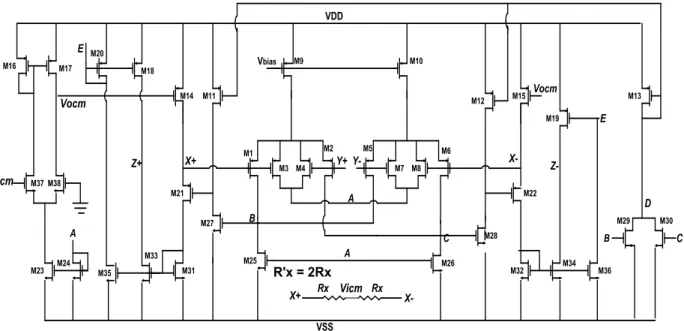
𝑉(𝐵)= 𝑉(𝐶)= (𝑖1𝑐𝑚+ 𝑖5𝑐𝑚− 𝑖25𝑐𝑚)𝑅𝑜𝑢𝑡𝐵= −𝜀𝑐4. 𝑅𝑜𝑢𝑡𝐵.
𝑔𝑚1
1 + 4𝑔𝑚1. 𝑟𝑜9(𝑉𝑖𝑛𝑐𝑚+ 𝑉𝑥𝑐𝑚) (8)
𝑉𝑑𝑀11= 𝑉𝑑𝑀12= (𝑖11𝑐𝑚− 𝑖27𝑐𝑚)𝑅𝑜𝑢𝑡𝑑𝑀11≅ (𝜀𝑐5+ 𝜀𝑐6)𝑅𝑜𝑢𝑡𝑑𝑀11. 𝑔𝑚27. 𝑉(𝐵) (9)
𝑉𝑥+𝑐𝑚= 𝑉𝑑𝑀11
𝑔𝑚21 𝑔𝑚31
𝑔𝑚31(𝑔𝑚21+ 𝑟𝑜21) − 𝑔𝑚31𝑟 + 𝑟𝑜21
𝑜14//𝑅𝑥
(10)
From Equations 8 to 10, common mode voltage gain to X-terminals is as follows:
𝐴𝑣𝑥𝑐𝑚= 𝑉𝑉𝑥𝑐𝑚
𝑖𝑛𝑐𝑚=
𝜀𝑐4(𝜀𝑐5+ 𝜀𝑐6) 𝑔𝑚21 𝑔𝑚31
𝑔𝑚31(𝑔𝑚21+ 𝑟𝑜21)− 𝑔𝑟𝑚31+ 𝑟𝑜21
𝑜14//𝑅𝑥
𝑔𝑚1.𝑔𝑚27𝑅𝑜𝑢𝑡(𝐵).𝑅𝑜𝑢𝑡(𝑑𝑀11)
1+ 4 𝑔𝑚1𝑟𝑜9
1 − 𝜀𝑐4(𝜀𝑐5+𝜀𝑐6) 𝑔𝑚21 𝑔𝑚31
𝑔𝑚31(𝑔𝑚21+ 𝑟𝑜21)− 𝑔𝑚31+𝑟𝑜21
𝑟𝑜14//𝑅𝑥
𝑔𝑚1.𝑔𝑚27𝑅𝑜𝑢𝑡(𝐵).𝑅𝑜𝑢𝑡(𝑑𝑀11)
1 + 4 𝑔𝑚1𝑟𝑜9
(11)
Now the total common mode voltage gain from Y-terminals to Z-terminals (while there are external resistor of 𝑅′𝑋 between X-terminals and external grounded loads of Rz at Z-terminals) can be concluded as Equation 11:
𝐴𝑣𝑧𝑐𝑚 =𝑖𝑧𝑐𝑚. 𝑅𝑧 𝑉𝑖𝑛𝑐𝑚 ≅
𝜀𝑐4(𝜀𝑐5+ 𝜀𝑐6)×(𝜀𝑐2+ 𝜀𝑐3−𝜀𝑐1) 𝑔𝑚1. 𝑔𝑚21. 𝑔𝑚27. 𝑅𝑜𝑢𝑡(𝐵).𝑅𝑜𝑢𝑡(𝑑𝑀11).𝑅𝑧
1 + 4 𝑔𝑚1𝑟𝑜9 (12)
Loop gain of feedback in the denominator of Equation 11 is very smaller than “one”, thus, can be ignored. Finally using Equations 6 and 12 gives voltage CMRR as Equation 13:
𝐶𝑀𝑅𝑅𝑉=
𝐴𝑣𝑧𝑑𝑖𝑓𝑓
𝐴𝑣𝑧𝑐𝑚 ≅
1 + 4 𝑔𝑚1𝑟𝑜9
𝜀𝑐4(𝜀𝑐5+ 𝜀𝑐6)×(𝜀𝑐2+ 𝜀𝑐3−𝜀𝑐1) 𝑔𝑚5. 𝑔𝑚21. 𝑔𝑚27.𝑅𝑜𝑢𝑡(𝐵).𝑅𝑜𝑢𝑡(𝑑𝑀11)(𝑅𝑥+ 𝑟𝑥)
(13)
Transistors dimensions of the proposed FDCCII is shown in Table 1. The dimensions have been optimized for loads of Rz+ = Rz- = RL=1 kΩ.
Table 1. Dimension of the transistors of the proposed FDCCII.
Transistors W/L (µm/µm)
M1-M8 6 / 0.45
M9-M10 24.8 / 0.8
M11-M13 1.26 / 0.45
M14-M15 5 / 0.5
M16-M17 8 / 1.7
M18-M19 0.47 / 0.6
M20 0.47 / 0.9
M23, M25-M26, M27-M28 6.48 / 1.53
M24 12.96 / 1.53
M29-M30 3.24 / 1.53
M31-M34 0.77 / 1.9
M35-M36 0.3 / 2
M37-M38 1.17 0.9
4- Proposed CMIA and Simulation Results
The novel FDCCII has been improved specifically towards the application of instrumentation amplifier. Thus it can be used alone as an IA when both of its Z-terminals are connected to a grounded load resistor RL. Configurations of the
proposed CMIA for voltage input case is shown in Figure 3.
Figure 3. CMIA configuration for voltage inputs.
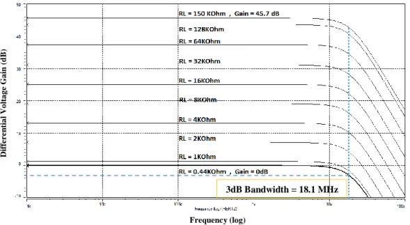
The most important specifications of the proposed circuit have been evaluated using HSPICE LEVEL 49 in 0.18 um TSMC CMOS Technology. It should be noticed that 𝑅′𝑋= 0.44 kΩand Vbias = 600 mV (bias voltage connected to gate
of M9 in Figure 2) has been used in the simulations. The results of the frequency response simulation at the several gains are shown in Figure 4 for voltage input case. Different gains are obtained (from 0 dB to 45.7 dB) using different values of the load resistors RL(RL =0.44KΩ-150KΩ). It can be seen that the BW is constant as 18.1MHz for different gains (the amount of RL to maintain thesame BW for differential voltage gain is limited to 150 KΩ). Favorably, Figure 4
shows that in the designed FDCCII there is no dependency between BW and gain, which exists in Voltage Mode (VM) circuits; the variation in the RL that results in the same variation in the voltage gain has no effect on the BW. The frequency responses of the voltage CMRR is shown in Figure 5. As it can be seen in Figure 5, the proposed CMIA has a CMRR of 216 dB with -3 dB BW of 300 Hz; with RL=1 KΩ, 𝑅′𝑋=0.44KΩ.
Figure 4. Frequency response of the voltage differential gains for different values of RL (.44KΩ-150KΩ).
D
iffe
r
e
n
ti
a
l
V
o
lta
g
e
G
a
in
(d
B)
Frequency (log)
Figure 5. Voltage CMRR for proposed CMIA with RL=1 KΩ, 𝑹′𝑿=0.44KΩ.
Table 2 summarizes the performance simulation results of the proposed CMIA. Differential voltage gain varies from 0dB (RL=0.44KΩ) to 45.7dB (RL=150KΩ). Power consumption under ±1.2V supply voltage is only 383.4 µW, and X-terminals intrinsic floating resistance (𝑟𝑥) is 45 Ω. The performance comparison between the proposed CMIA and some other artworks is summarized in Table 3.
Table 2. CMIA's performance specifications.
Voltage CMRR 216 dB
CMRR 3dB Bandwidth 300 Hz
Differential Voltage Gain Bandwidth (RL≤150KΩ) 18.1MHz
Differential Voltage Gain(0.44KΩ ≤RL≤ 150KΩ) 0 dB - to – 45.7 dB
Differential Voltage Gain Bandwidth product(MHz) 18.1 * 106 -to- 3.49 * 109
Power Dissipation 383.4 µW
Supply Voltages ±1.2V
X-terminals intrinsic floating resistance (𝒓𝒙) 45 Ω
As it can be seen in Table 3, the proposed CMIA exhibits superior performance in terms of CMRRvalue and differential gain BW for voltage input, very low (𝑟𝑥) and low consumed power. Also, it doesn't need matched blocks.
Table 3. Comparison between the proposed CMIA and some other works
c for current input, v for voltage input, e not available
Specification [18] [17] [17] [8] [11] [13] Proposed
Input Signal Voltage Voltage Voltage Voltage Voltage Current Voltage
Technology 65 nm CMOS 130 nm CMOS 90 nm CMOS 0.18um CMOS 0.35um CMOS 0.18um CMOS 0.18 um CMOS
CMRR 88 dBv 64.7 dBv 76 dBv 110 dBv 107 dBv 91 dBc 216 dB
CMRR
Bandwidth < 6 KHz 100 KHz 14 KHz NA
e NAe 1.15 kHzc 300 Hz
Differential
Voltage Gain <39 dB < 61 dB < 50 dB 0 dB 0 dB 0 dB 0 dB-to- 45.7dB
Differential Gain BW
product
NAe < 381 MHz <56.9 MHz NAe 8 MHzv 10.18 MHzc 18.1 MHz to
3.49 GHz
Power
Dissipation 3.96 µW 14 µW 11 µW 420 µW 1.3 mW 219 ~ 446 µW 383.4 µW
Supply Voltages 1.2 V 0.4 V 0.4 V ±1.65 V ±1.5 V ±0.8 V ±1.2 V
Needs Matched
Blocks Yes No No Yes No No No
Frequency (log)
V
o
lta
g
e
C
M
R
R
(
dB
10- Conclusion
In this paper, a novel topology of a low power, very high CMRR, and wide BW CMIA is introduced. Its structure is based on one active block named FDCCII, which is designed based on novel structures and techniques, that eliminates the need for well-matched blocks to reach a very high CMRR for the proposed CMIA. The results of HSPICE simulations show that the CMRR value and BW as the most important properties of CMIAs, are greatly improved using CMFB and CMFF techniques. Because of its low power dissipation it can also be used for portable systems and well matched the down scale trend of the modern technologies.
12- References
[1] A.J. Annema, B. Nauta, R.V. Langevelde, H. Tuinhout, Analogue circuits in ultra-deep- submicron CMOS. IEEE J. Solid-State Circuits, Vol. 40, 2005, pp.132–143. DOI: 10.1109/JSSC.2004.837247.
[2] C. Toumazou, F. J. Lidgey, and D. G. Haigh, Analogue IC Design: The Current-Mode Approach, London, U.K., IEE Press, 1990. [3] G. Ferri and N.C. Guirrini, Low-Voltage, Low-Power CMOS Current Conveyors (Chap.4), Kluwer 2003.
[4] Archana, S., B. K. Madhavi, and IV Murali Krishna. "Design of CMOS current mode and voltage mode Winner Take all circuit on 180nm technology." Electrical, Electronics, and Optimization Techniques (ICEEOT), International Conference on. IEEE, 2016. DOI: 10.1109/ICEEOT.2016.7755014.
[5] Broomandnia, Hassan, and Seyed Javad Azhari. "Design of a fully differential current buffer (FDCB) based on a new common mode feedforward (CMFF) based common mode separation technique." Knowledge-Based Engineering and Innovation (KBEI), 2015 2nd International Conference on. IEEE, 2015. DOI: 10.1109/KBEI.2015.7436074.
[6] E. L. Douglas et al., A low-voltage current-mode instrumentation amplifier designed in a 0.18-micron CMOS technology, in Proc. IEEE CCECE-CCGEI, May. 2004, pp. 1777-1780. DOI: 10.1109/CCECE.2004.1349760.
[7] S.J.Azhari, and H.Fazlalipoor, CMRR in Voltage-Op-Amp-Based Current-Mode Instrumentation Amplifiers (CMIA), IEEE TRANSACTIONS ON INSTRUMENTATION AND MEASUREMENT, VOL. 58, 2009, pp. 563-569. DOI: 10.1109/TIM.2008.2005559.
[8] A. Voulkidou, S. Siskos, and T. Laopoulos, A Low Noise Low Offset Current Mode Instrumentation Amplifier, 19th International Conference Mixed Design of Integrated Circuits and Systems, May 24-26, 2012, pp. 203-207.
[9] B.Babaei and S.Mirzakuchaki, High CMRR, Low Power and Wideband Current-Mode Instrumentation Amplifier, in Proc. IEEE Int. Norchip Conference, 2006, pp.3-4. DOI: 10.1109/NORCHP.2006.329258.
[10] S.J. Azhari and H. Fazlalipoor, A novel current mode instrumentation amplifier (CMIA) topology, IEEE Transactions on Instrumentation and Measurement, 49, 2000, pp. 1272-1277. DOI: 10.1109/19.893269.
[11] A.A. SILVERIO, R.S. J. REYES, and W.Y. CHUNG, A Low Power High CMRR CMOS Instrumentation Amplifier Based on Differential Voltage – Current Conveyor for Beta-Dispersion Range Bio-Impedance Applications, Recent Researches in Circuits, Systems, Multimedia and Automatic Control, 2012, pp.31-36.
[12] A. Panchal, P.K. Jain, and D.S. Ajnar, Instrumentation Amplifier using Differential voltage second generation current conveyor (DVCCII) in standard 0.18 μm CMOS technology, International Journal of Engineering Science and Technology (IJEST), Vol. 3, 2011.
[13] L. Safari, and Sh. Minaei, A Novel Resistor-Free Electronically Adjustable Current-Mode Instrumentation Amplifier, Circuits, Systems, and Signal Processing, Vol. 32, Issue. 3, June 2013, pp 1025-1038. DOI https://doi.org/10.1007/s00034-012-9522-y. [14] Safari, Leila, and Shahram Minaei. "New ECCII-based electronically controllable current-mode instrumentation amplifier with
high frequency performance." Circuit Theory and Design (ECCTD), 2017 European Conference on. IEEE, 2017. DOI: 10.1109/ECCTD.2017.8093343.
[15] Das, Devarshi Mrinal, et al. "Design considerations for high-cmrr low-power current mode instrumentation amplifier for biomedicai data acquisition systems." Electronics, Circuits and Systems (ICECS), 2014 21st IEEE International Conference on. IEEE, 2014. DOI: 10.1109/ICECS.2014.7049969.
[16] M'Harzi, Zineb, Mustapha Alami, and Farid Temcamani. "A novel high bandwidth current mode instrumentation amplifier." Microelectronics (ICM), 2015 27th International Conference on. IEEE, 2015. DOI: 10.1109/ICM.2015.7438048.
[17] Eldeeb, Mohammed A., et al. "A 0.4-V Miniature CMOS Current Mode Instrumentation Amplifier." IEEE Transactions on Circuits and Systems II: Express Briefs 65.3 (2018): 261-265. DOI: 10.1109/TCSII.2017.2685589.
[19] Kumngern, Montree, and Fabian Khateb. "A low-voltage and low-power multiple-input floating-gate FDCCII." Electrical Engineering/Electronics, Computer, Telecommunications and Information Technology (ECTI-CON), 2015 12th International Conference on. IEEE, 2015. DOI: 10.1109/ECTICon.2015.7206943.
[20] E.A. Sobhy and A.M. Soliman, Realizations of fully differential voltage second generation current conveyor with an application, International Journal of Circuit Theory and Applications; Vol. 38, Issue. 5, 2010, pp. 441-452. DOI: 10.1002/cta.566.
[21] Suwansawang, Sopapun, and Thawatchai Thongleam. "A 1-V bulk-driven CMOS fully differential second-generation current conveyor." Intelligent Signal Processing and Communications Systems (ISPACS), 2013 International Symposium on. IEEE, 2013. DOI: 10.1109/ISPACS.2013.6704631.
[22] Caviglia, Stefano, et al. "A high-linearity design for rail-to-rail fully differential current conveyors." Electronics, Circuits and Systems (ICECS), 2014 21st IEEE International Conference on. IEEE, 2014. DOI: 10.1109/ICECS.2014.7050044.
[23] Malik, Shahid, et al. "A CCII-based relaxation oscillator as a versatile interface for resistive and capacitive sensors." Signal Processing and Integrated Networks (SPIN), 2016 3rd International Conference on. IEEE, 2016. DOI: 10.1109/SPIN.2016. 7566719.
[24] Choubey, Chandan Kumar, Gaurav Tiwari, and Sajal K. Paul. "CCII based multifunction inverse filter." Advances in Electronics, Communication and Computer Technology (ICAECCT), 2016 IEEE International Conference on. IEEE, 2016. DOI: 10.1109/ICAECCT.2016.7942574.
[25] Kumngern, Montree. "Three-input single-output voltage-mode universal filter using single FDCCII." Intelligent Signal Processing and Communication Systems (ISPACS), 2014 International Symposium on. IEEE, 2014. DOI: 10.1109/ISPACS.2014.7024469.
![Figure 1. Block diagram of FDCCII. [ i y+iy−vx+vx−iz+i z− ] = [ 001000 0 0 0 −1 0 0 0 0 0 0 1 0 0 0 0 0 0 0 0 0 0 0 0 −1000 0 0 0 ] [ v y+vy−ix+ix−vZ+vZ− ] (1)](https://thumb-us.123doks.com/thumbv2/123dok_us/7935455.2109671/2.893.332.562.87.226/figure-block-diagram-fdccii-ix-ix-vz-vz.webp)