www.sii-ic.com
SUPER-LOW CURRENT CONSUMPTION 150 mA VOLTAGE REGULATOR WITH
BUILT-IN HIGH-ACCURACY VOLTAGE DETECTOR AND RESET INPUT FUNCTION
© Seiko Instruments Inc., 2008-2012
Rev.2.1
_00The S-1702 Series, developed based on CMOS technology, is a 150 mA output positive voltage regulator with a low dropout voltage, a high-accuracy output voltage, and low current consumption.
The S-1702 Series includes a voltage regulator with high-accuracy output voltage of ±1.0% allowing to use a ceramic capacitor of 1.0 μF or more, and a voltage detector that monitors the output/input voltage of the regulator. It also includes an overcurrent protector that prevents the output current from exceeding the current capacitance of the output transistor and an output forcible discharge circuit for the regulator operation off.
Small SNT-6A package is available for the S-1702 Series. And an external small capacitor can be used, enabling high-density mounting. Its super-low current consumption makes the S-1702 Series ideal for mobile devices.
Features
Regulator block
•Output voltage: 1.5 V to 5.5 V, selectable in 0.05 V step
•High-accuracy output voltage: ±1.0%
• Super-low current consumption: Current consumption of regulator block: 9 μA typ., 16 μA max.
•High peak current capability: 150 mA output (VIN≥ VOUT(S)+ 1.0 V)*1
• Built-in on/off discharge circuit: Longer battery life, discharges output load instantaneously
•High ripple rejection: 70 dB typ. (1.0 kHz)
•Built-in overcurrent protector: Limits overcurrent of output transistor
Detector block
•Output voltage: 1.3 V to 5.2 V, selectable in 0.05 V step
•Built-in high-accuracy voltage detector: ±1.0%
Monitoring output/input or monitoring external input by option (detector output)
•External reset input: Forcible assertion of detector output by external reset pin (RESX) input
Overall
•Correlation temperature gradient in the regulator and the detector blocks
•Super-low current consumption: During operation*2: 10 μA typ., 18 μA max.
•Operation temperature range: Ta = −40°C to +85°C
•Lead-free, Sn 100%, halogen-free*3
*1. Attention should be paid to the power dissipation of the package when the output current is large. *2. Excluding current flowing in pull-up and pull-down resistors connected to the ON / OFF or RESX pins *3. Refer to “ Product Name Structure” for details.
Applications
• Wireless power supply circuit block for cellular phone
• Power supply circuit block for health care product
• Power supply circuit block for various mobile devices
Package
• SNT-6A
Block Diagrams
1. S-1702 Series A type to H type
Discharge Shunt Function by ON / OFF and RESX
Pins Product Type Detector Monitor Voltage Control by ON / OFF Pin Control by RESX Pin A VOUT { { B VOUT { × C VOUT × { D VOUT × × E VIN { { F VIN { × G VIN × { H VIN × × Overcurrent protector ON/OFF circuit Reference voltage circuit Reference voltage circuit ON / OFF VIN RESX VOUT VSS VDOUT Reset circuit Delay circuit Voltage detector Output circuit Logic circuit Figure 1
2. S-1702 Series J type and K type (external input detection type)
ProductType
Detector Monitor Voltage
Discharge Shunt Function by ON / OFF Pin J External input { K External input × Overcurrent protector ON/OFF circuit Reference voltage circuit ON / OFF VIN SENSE VOUT VSS VDOUT Delay circuit Voltage detector Reset circuit Logic circuit Reference voltage circuit Output circuit Figure 2
3. S-1702 Series L type to N type, P type (external delay type)
Product Type Detector Monitor VoltageDischarge Shunt Function by ON / OFF Pin L VOUT { M VOUT × N VIN { P VIN × Overcurrent protector ON/OFF circuit Reference voltage circuit ON / OFF VIN CD VOUT VSS VDOUT Delay circuit Voltage detector Reset circuit Logic circuit Reference voltage circuit Output circuit Figure 3
Product Name Structure
1. Product name
S-1702 x x x xx - I6T1 x
Environmental code
U : Lead-free (Sn 100%), halogen-free
G : Lead-free (for details, please contact our sales office) Package abbreviation and IC packing specifications*1
I6T1: SNT-6A, tape product
Output voltage value of regulator and detection voltage value of detector*2 00 and 01 (two-digit numeric option code)
Input type of RESX and ON / OFF pins*3
A to H, J (one-digit alphabetical option code) Output type of VDOUT pin*4
A to H, J (one-digit alphabetical option code) Product type*5
A to H, J to N, P (one-digit alphabetical option code)
*1. Refer to the tape drawing.
*2. Refer to Table 4 of “2. Function list according to product type”.
*3. Refer to Table 3 of “2. Function list according to product type”.
*4. Refer to Table 2 of “2. Function list according to product type”.
2. Function list according to product type
Table 1 Product Types
Discharge Shunt Function Option
Code
ON / OFF Pin Application
RESX Pin
Application Delay Type
Detector Monitor
Voltage Control by
ON / OFF Pin Control by RESX Pin
A ON / OFF RESX Internal VOUT { {
B ON / OFF RESX Internal VOUT { ×
C ON / OFF RESX Internal VOUT × {
D ON / OFF RESX Internal VOUT × ×
E ON / OFF RESX Internal VIN { {
F ON / OFF RESX Internal VIN { ×
G ON / OFF RESX Internal VIN × {
H ON / OFF RESX Internal VIN × ×
J ON / OFF SENSE Internal VSENSE { –
K ON / OFF SENSE Internal VSENSE × –
L ON / OFF CD External VOUT { –
M ON / OFF CD External VOUT × –
N ON / OFF CD External VIN { –
P ON / OFF CD External VIN × –
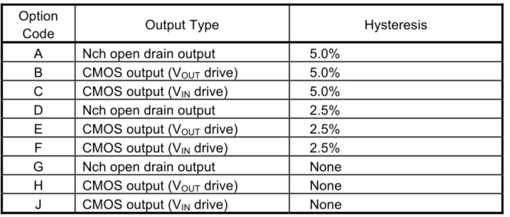
Table 2 Output Types of VDOUT Pin Option
Code Output Type Hysteresis
A Nch open drain output 5.0% B CMOS output (VOUT drive) 5.0% C CMOS output (VIN drive) 5.0% D Nch open drain output 2.5% E CMOS output (VOUT drive) 2.5% F CMOS output (VIN drive) 2.5% G Nch open drain output None H CMOS output (VOUT drive) None J CMOS output (VIN drive) None
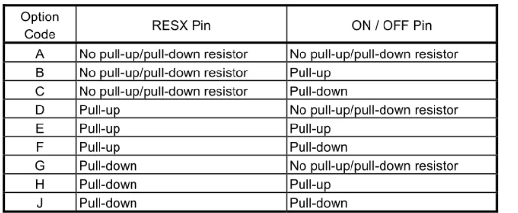
Table 3 Input Types of RESX and ON / OFF Pins Option
Code RESX Pin ON / OFF Pin
A No pull-up/pull-down resistor No pull-up/pull-down resistor B No pull-up/pull-down resistor Pull-up
C No pull-up/pull-down resistor Pull-down
D Pull-up No pull-up/pull-down resistor
E Pull-up Pull-up
F Pull-up Pull-down
G Pull-down No pull-up/pull-down resistor
H Pull-down Pull-up
J Pull-down Pull-down
Table 4 Output Voltage Values of Regulator and Detection Voltage Values of Detector Option
Code Output Voltage Detection Voltage
00 3.1 V ±1.0% 2.75 V ±1.0%
01 3.1 V ±1.0% 2.60 V ±1.0%
Remark Please contact our sales office for products with an output voltage or detection
voltage other than those specified above.
3. Package
Drawing Code Package Name
Package Tape Reel Land
Pin Configuration
1.
SNT-6A
Table 5
Pin No. Symbol Description
1 VIN Input voltage pin 2 ON / OFF Power-off pin
RESX External reset pin (S-1702Axx to Hxx)
CD External delay capacitor connection pin (S-1702Lxx to Nxx, Pxx)
3
SENSE Detector SENSE pin (S-1702Jxx, Kxx)
4 VSS GND pin
5 VDOUT Detector output voltage pin 6 VOUT Regulator output voltage pin
5 4 6 2 3 1 Top view Figure 4
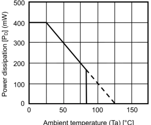
Absolute Maximum Ratings
Table 6
(Ta = +25°C unless otherwise specified)
Item Symbol Absolute Maximum Rating Unit
VIN VSS− 0.3 to VSS+ 7.0 V VON / OFF VSS− 0.3 to VIN+ 0.3 V VRESX VSS− 0.3 to VIN+ 0.3 V VCD VSS− 0.3 to VIN+ 0.3 V Input voltage VSENSE VSS− 0.3 to VSS+ 7.0 V
Regulator output voltage VOUT VSS− 0.3 to VIN+ 0.3 V
Nch open drain output VSS− 0.3 to VSS+ 7.0 V Detector output
voltage CMOS output VDOUT VSS− 0.3 to VIN+ 0.3 V
Power dissipation PD 400*1 mW
Operation ambient temperature Topr −40 to +85 °C
Storage temperature Tstg −40 to +125 °C
*1. When mounted on board [Mounted board]
(1) Board size : 114.3 mm × 76.2 mm × t1.6 mm (2) Board name : JEDEC STANDARD51-7
Caution The absolute maximum ratings are rated values exceeding which the product could suffer
physical damage. These values must therefore not be exceeded under any conditions.
Ambient temperature (Ta) [°C]
0 50 100 150 300 100 0 500 200 400 Pow er dis sip ation [P D ] ( m W)
Electrical Characteristics
1. Common to series (S-1702Axx to Hxx, Jxx to Nxx, Pxx)
Table 7 (1 / 2)Entire circuit (Ta = +25°C unless otherwise specified)
Item Symbol Condition Min. Typ. Max. Unit Test
Circuit Current consumption during operation*1 ISS VIN = VOUT(S)+ 1.0 V – 10 18 μA 2 Regulator block
Item Symbol Condition Min. Typ. Max. Unit CircuitTest
Output voltage*2 V
OUT(E) VIN = VOUT(S)+ 1.0 V, IOUT = 30 mA V×OUT(S)0.99 VOUT(S) V×OUT(S)1.01 V 1 Output current*3 I OUT VIN > VOUT(S)+ 1.0 V 150*8 – – mA 3 1.5 V < VOUT(S)≤ 2.0 V – 0.54 0.58 V 1 2.0 V < VOUT(S)≤ 2.5 V – 0.23 0.35 V 1 2.5 V < VOUT(S)≤ 3.0 V – 0.2 0.3 V 1 3.0 V < VOUT(S)≤ 3.3 V – 0.15 0.23 V 1 Dropout voltage*4 V drop IOUT = 100 mA 3.3 V < VOUT(S)≤ 5.5 V – 0.14 0.21 V 1 Line regulation ΔVIN• VOUT ΔVOUT1 VOUT(S)+ 0.5 V < VIN < 6.5 V, IOUT = 30 mA – 0.05 0.2 %/V 1
Load regulation ΔVOUT2 VIN = VOUT(S)+ 1.0 V,
10 μA < IOUT < 100 mA – 20 40 mV 1 Output voltage temperature coefficient *5 ΔTa • VOUT ΔVOUT VIN = VOUT(S)+ 1.0 V, IOUT = 30 mA, −40°C ≤ Ta ≤+85°C*9 – ±100 ±300 ppm/ °C 1 Current consumption during operation*1 ISS1 VIN = VOUT(S)+ 1.0 V,
RESX and ON / OFF pins enabled for operation, no load
– 9 16 μA 2
Input voltage VIN – 2 – 6.5 V –
ON / OFF pin
input voltage “H” VSH1 VIN = VOUT(S)+ 1.0 V, RL = 1.0 kΩ 1.2 – – V 4 ON / OFF pin
input voltage “L” VSL1 VIN = VOUT(S)+ 1.0 V, RL = 1.0 kΩ – – 0.3 V 4
S-1702xxA −0.1 – 0.1 μA 4
S-1702xxD −0.1 – 0.1 μA 4
ON / OFF pin
input current “H” ISH1 VIN = 6.5 V, VON / OFF = 6.5 V
S-1702xxG −0.1 – 0.1 μA 4
S-1702xxA −0.1 – 0.1 μA 4
S-1702xxD −0.1 – 0.1 μA 4
ON / OFF pin
input current “L” ISL1 VIN = 6.5 V, VON / OFF = 0 V
S-1702xxG −0.1 – 0.1 μA 4 1.5 V ≤ VOUT(S) < 3.1 V – 70 – dB 5 Ripple rejection RR VIN = VOUT(S)+ 1.0 V, f = 1.0 kHz, ΔVrip = 0.5 Vrms, IOUT = 30 mA 3.1 V ≤ VOUT(S)≤ 5.5 V – 65 – dB 5 Short-circuit current ISHORT VIN = VOUT(S)+ 1.0 V,
ON / OFF pin enabled for operation, VOUT = 0 V
Table 7 (2 / 2)
Detector block (Ta = +25°C unless otherwise specified)
Item Symbol Condition Min. Typ. Max. Unit Test
Circuit
Detection voltage*6 −VDET – −×VDET(S)
0.99 −VDET(S) −VDET(S) ×1.01 V 6 S-1702xAx, S-1702xBx, S-1702xCx ×−VDET 0.035 −VDET ×0.05 −VDET ×0.065 V 6 S-1702xDx, S-1702xEx, S-1702xFx −VDET ×0.01 −VDET ×0.025 −VDET ×0.04 V 6
Hysteresis width VHYS
S-1702xGx, S-1702xHx, S-1702xJx – 0 −VDET ×0.015 V 6 VIN = −VDET(S)+ 1.5 V – 2.4 4.0 μA 2 1.3 V ≤−VDET(S) < 2.3 V VIN = 5.5 V – 2.6 4.5 μA 2 VIN = −VDET(S)+ 1.5 V – 2.2 3.5 μA 2 Current consumption during operation*1 ISS2 2.3 V ≤−VDET(S) < 5.2 V VIN = 5.5 V – 2.3 4.0 μA 2 Input voltage VIN – 0.8 – 6.5 V – Detection voltage temperature coefficient *7 ΔTa • −VDET Δ−VDET Ta = −40°C to +85°C*9 – ±100 ±400 ppm/ °C 6 *1. Excluding current flowing in pull-up and pull-down resistors connected to the ON / OFF or RESX pins
*2. VOUT(S): Set output voltage
VOUT(E): Actual output voltage at the fixed load
The output voltage when fixing IOUT (= 30 mA) and inputting VOUT(S)+ 1.0 V
*3. The output current at which the output voltage becomes 95% of VOUT(E) after gradually increasing the output current. *4. Vdrop = VIN1− (VOUT3× 0.98)
VOUT3 is the output voltage when VIN = VOUT(S)+ 1.0 V and IOUT = 100 mA.
VIN1 is the input voltage at which the output voltage becomes 98% ofVOUT3 after gradually decreasing the input voltage.
*5. The change in temperature [mV/°C] of the regulator output voltage is calculated using the following equation.
ΔTa • VOUT ΔVOUT [mV/°C]*1= VOUT(S) [V]*2 × ΔVOUT [ppm/°C]*3 ÷ 1000 ΔTa
*1. The change in temperature of the output voltage *2. Set output voltage
*3. Output voltage temperature coefficient *6. −VDET(S) : Set detection voltage
−VDET : Actual detection voltage
*7. The change in temperature [mV/°C] of the detector detection voltage is calculated using the following equation.
ΔTa • −VDET Δ−VDET [mV/°C]*1= −V DET(S) (Typ.) [V]*2 × Δ−VDET [ppm/°C]*3 ÷ 1000 ΔTa
*1. The change in temperature of the detection voltage *2. Set detection voltage
*3. Detection voltage temperature coefficient *8. The output current can be at least this value.
Due to restrictions on the package power dissipation, this value may not be satisfied. Attention should be paid to the power dissipation of the package when the output current is large. This specification is guaranteed by design. *9. Since products are not screened at high and low temperatures, the specification for this temperature range is
2. Discharge shunt circuit (discharge shunt function) (S-1702Axx, Bxx, Cxx, Exx, Fxx, Gxx, Jxx, Lxx, Nxx)
Table 8(Ta = +25°C unless otherwise specified)
Item Symbol Condition Min. Typ. Max. Unit Test
Circuit “L” output, Nch on resistor RLOW VDS = 0.5 V, VGS = 6.5 V – 100 – Ω 3
3. Detector output circuit (VDOUT pin)
Table 9
Nch open drain output (S-1702xAx, xDx, xGx) (Ta = +25°C unless otherwise specified)
Item Symbol Condition Min. Typ. Max. Unit Test
Circuit Output current IDOUT1 Output transistor: Nch,
VDS = 0.5 V, VDD = 1.2 V 1.36 2.55 – mA 7 Leakage current ILEAK Output transistor: Nch,
VDS = 5.5 V, VDD = 5.5 V – – 100 nA 7
CMOS output (S-1702xBx, xCx, xEx, xFx, xHx, xJx)
Item Symbol Condition Min. Typ. Max. Unit Test
Circuit IDOUT2 Output transistor: Nch,
VDS = 0.5 V, VIN = 1.2 V 1.36 2.55 – mA 7 Output current
IDOUT3 Output transistor: Pch,
VDS = 0.5 V, VIN = 5.5 V 1.71 2.76 – mA 8
4. RESX pin (S-1702Axx, Bxx, Cxx, Dxx, Exx, Fxx, Gxx, Hxx)
Table 10(Ta = +25°C unless otherwise specified)
Item Symbol Condition Min. Typ. Max. Unit Test
Circuit RESX pin input voltage “H”*1 V
SH2 VIN = VOUT(S)+ 1.0 V, RL = 1.0 kΩ 1.2 – – V 4 RESX pin input voltage “L” VSL2 VIN = VOUT(S)+ 1.0 V, RL = 1.0 kΩ – – 0.3 V 4
S-1702xxA −0.1 – 0.1 μA 4
S-1702xxB −0.1 – 0.1 μA 4
RESX pin input current “H” ISH2 VIN = 6.5 V, VRESX = 6.5 V
S-1702xxC −0.1 – 0.1 μA 4
S-1702xxA −0.1 – 0.1 μA 4
S-1702xxB −0.1 – 0.1 μA 4
RESX pin input current “L” ISL2 VIN = 6.5 V, VRESX = 0 V
S-1702xxC −0.1 – 0.1 μA 4
*1. VOUT(S): specified output voltage value
5. Pull-up / pull-down resistor value of ON / OFF pin and RESX pin (S-1702xxB, xxC, xxD, xxE, xxF xxG, xxH, xxJ)
Table 11(Ta = +25°C unless otherwise specified)
Item Symbol Condition Min. Typ. Max. Unit Test
Circuit
6. Response time
Table 12
Internal delay type (S-1702Axx, Bxx, Cxx, Dxx, Exx, Fxx, Gxx, Hxx, Jxx, Kxx) (Ta = +25°C unless otherwise specified)
Item Symbol Condition Min. Typ. Max. Unit Test
Circuit
Response time TPLH1 – – – 90 μs 6
External delay type (S-1702Lxx, Mxx, Nxx, Pxx)
Item Symbol Condition Min. Typ. Max. Unit Test
Circuit
Test Circuits
1.
VIN VOUT VDOUT VSS RESX V + A + Set to power on ON / OFF A +The portion enclosed by dotted lines is not required for CMOS output products.
2.
VIN VOUT VDOUT VSS RESX Set to VIN or GND ON / OFF A +The portion enclosed by dotted lines is not required for CMOS output products.
Figure 6 Figure 7
3.
VIN VOUT VDOUT VSS RESX V + Set to VIN or GND ON / OFF A +The portion enclosed by dotted lines is not required for CMOS output products.
A +
4.
VIN VOUT VDOUT VSS RESX V + ON / OFFThe portion enclosed by dotted lines is not required for CMOS output products.
A + A + RL Figure 8 Figure 9
5.
VIN VOUT VDOUT VSS RESX V + ON / OFFThe portion enclosed by dotted lines is not required for CMOS output products.
RL Set to power on
6.
VIN VOUT VDOUT VSS RESX (SENSE) ON / OFFThe portion enclosed by dotted lines is not required for CMOS output products.
V + Figure 10 Figure 11
7.
VIN VOUT VDOUT VSS RESX + ON / OFF + V A V DS8.
VIN VOUT VDOUT VSS RESX + ON / OFF V + A VDS Figure 12 Figure 139.
VIN VOUT VDOUT VSS RESX (CD) ON / OFFThe portion enclosed by dotted lines is not required for CMOS output products.
V
+
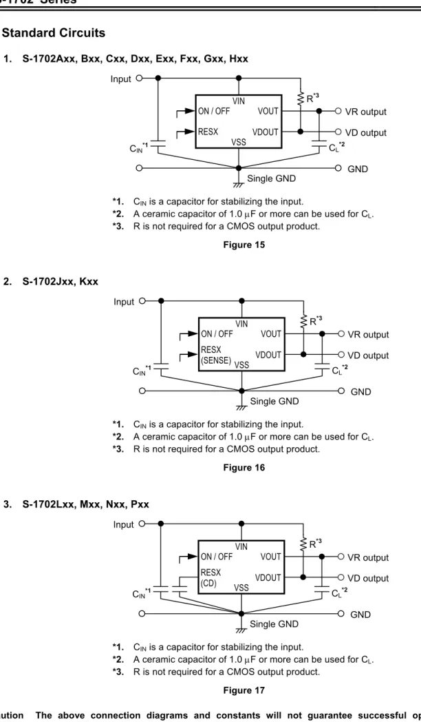
Standard Circuits
1. S-1702Axx, Bxx, Cxx, Dxx, Exx, Fxx, Gxx, Hxx
VIN VOUT VDOUT VSS RESX ON / OFF VR output VD output GND Single GND Input CL*2 CIN*1 R*3*1. CIN is a capacitor for stabilizing the input.
*2. A ceramic capacitor of 1.0 μF or more can be used for CL. *3. R is not required for a CMOS output product.
Figure 15
2. S-1702Jxx, Kxx
VIN VOUT VDOUT VSS RESX (SENSE) ON / OFF VR output VD output GND Single GND Input CL*2 CIN*1 R*3*1. CIN is a capacitor for stabilizing the input.
*2. A ceramic capacitor of 1.0 μF or more can be used for CL. *3. R is not required for a CMOS output product.
Figure 16
3. S-1702Lxx, Mxx, Nxx, Pxx
VIN VOUT VDOUT VSS RESX (CD) ON / OFF VR output VD output GND Single GND Input CL*2 CIN*1 R*3*1. CIN is a capacitor for stabilizing the input.
*2. A ceramic capacitor of 1.0 μF or more can be used for CL. *3. R is not required for a CMOS output product.
Figure 17
Caution The above connection diagrams and constants will not guarantee successful operation. Perform thorough evaluation using the actual application to set the constants.
Application Conditions
Input capacitor (CIN): 1.0 μF or more Output capacitor (CL): 1.0 μF or more ESR of output capacitor: 10 Ω or less
Caution Generally a series regulator may cause oscillation, depending on the selection of external parts. Confirm that no oscillation occurs in the application for which the above capacitors are used.
Selection of VIN Input and VOUT Output Capacitors (CIN, CL)
The S-1702 Series requires an output capacitor (CL) between the VOUT and VSS pins for phase compensation. A ceramic capacitor with a capacitance of 1.0 μF or more provides a stable operation in all temperature ranges. When using an OS capacitor, tantalum capacitor, or aluminum electrolytic capacitor, a capacitor with a capacitance of 1.0 μF or more and an ESR of 10 Ω or less is required.
The output overshoot and undershoot values, which are transient response characteristics, vary depending on the output capacitor value. The required capacitance value for the input capacitor differs depending on the application. The recommended application values are CIN = 1.0 μF or more and CL = 1.0 μF or more; however, perform thorough evaluation using the actual device, including evaluation of temperature characteristics.
Explanation of Terms
1. Regulator block
1. 1 Low dropout voltage regulator
This voltage regulator has the low dropout voltage due to its built-in transistor with low on-resistance.
1. 2 Low ESR
A capacitor whose ESR (Equivalent Series Resistance) is low. The S-1702 Series enables use of a low ESR capacitor, such as a ceramic capacitor, for the output-side capacitor (CL). A capacitor whose ESR is 10 Ω or less can be used.
1. 3 Output voltage (VOUT)
The accuracy of the output voltage is ensured at ±1.0% under the specified conditions of fixed input voltage*1, fixed output current, and fixed temperature.
*1. Differs depending on the product.
Caution If the above conditions change, the output voltage value may vary and exceed the accuracy
range of the output voltage. Refer to “ Electrical Characteristics” and “ Characteristics
(Typical Data)” for details.
1. 4 Line regulation
⎟
⎠
⎞
⎜
⎝
⎛
•
Δ
Δ
OUT IN 1 OUTV
V
V
Indicates the dependency of the output voltage on the input voltage. That is, the values show how much the output voltage changes due to a change in the input voltage with the output current remaining unchanged.
1. 5 Load regulation (ΔVOUT2)
Indicates the dependency of the output voltage on the output current. That is, the values show how much the output voltage changes due to a change in the output current with the input voltage remaining unchanged.
1. 6 Dropout voltage (Vdrop)
Indicates the difference between the input voltage VIN1, which is the input voltage (VIN) at the point where the output voltage has fallen to 98% of the output voltage value VOUT3 after VIN was gradually decreased from VIN = VOUT(S)+ 1.0 V, and the output voltage at that point (VOUT3× 0.98).
1. 7 Output voltage temperature coefficient
⎟
⎠
⎞
⎜
⎝
⎛
•
Δ
Δ
OUT OUTV
Ta
V
The shaded area in Figure 18 is the range where VOUT varies in the operating temperature range when the output voltage temperature coefficient is ±100 ppm/°C.
(Refer to *5 of Table 7 for how to calculate the temperature change [mV/°C] of the output voltage.)
*1. VOUT(E) is the value of the output voltage measured at 25°C.
VOUT(E)*1 −40 25 +0.30 mV/°C VOUT [V] 85 Ta [°C] −0.30 mV/°C
2. Detector block
2. 1 Detection voltage (−VDET)
The detection voltage (−VDET) is a voltage when the detector output voltage (VDOUT) switches to low. This detection voltage varies slightly depending on products even having the same specification. The range between the minimum (−VDET) value and the maximum (−VDET) value due to variation is called the range of detection voltage (refer to Figure 19).
e.g. In a product with −VDET = 3.0 V, the detection voltage is a value in the range of 2.97 V ≤ (−VDET) ≤ 3.03 V. This means that some products have 2.97 V for −VDET and some have 3.03 V.
Detection voltage
Range of detection voltage VOUT
(−VDET) min.
(−VDET) max.
VDOUT
Remark This is the case when the regulator output voltage (VOUT) is monitored by the detector.
Figure 19 Detection Voltage (−VDET)
2. 2 Release voltage (+VDET)
The release voltage (+VDET) is a voltage when the detector output voltage (VDOUT) switches to high. This release voltage varies slightly depending on products even having the same specification. The range between the minimum (+VDET) value and the maximum (+VDET) value due to variation is called the range of release voltage (refer to Figure 20).
e.g. In a product with −VDET = 3.0 V and hysteresis width of 5%, the release voltage is a value in the range of 3.074 V ≤ (+VDET) ≤ 3.227 V.
This means that some products have 3.074 V for +VDET and some have 3.227 V.
Range of release voltage VOUT Delay time Release voltage (+VDET) min. (+VDET) max. VDOUT
Remark This is the case when the regulator output voltage (VOUT) is monitored by the detector.
2. 3 Hysteresis width (VHYS)
The hysteresis width is the difference between the detection voltage and the release voltage. Setting the hysteresis width prevents malfunction caused by noise on the input voltage. The hysteresis width is internally fixed and varies depending on the product type (refer to Table 2).
2. 4 Delay time (tD)
The delay time (tD) is a period from the input voltage flowing to the detector block has exceeded the release voltage (+VDET), until the detector output voltage (VDOUT) inverts.
The internal delay type products (S-1702Axx, Bxx, Cxx, Dxx, Exx, Fxx, Gxx, Hxx, Jxx, Kxx) have delay time which is internally fixed.
In external delay type products (S-1702Lxx, Mxx, Nxx, Pxx), the delay time (tD) can be changed by controlling the capacitance value of the capacitor (CD) connected between the CD (RESX) and VSS pins.
For how to set the delay time (tD), refer to “3. 2 Delay circuit” in “3. Detector block” in“ Operation”.
tD VOUT VDOUT When tD = 90 μs V +VDET tD When tD = 30 ms t
Remark This is the case when the regulator output voltage (VOUT) is monitored by the detector.
Figure 21
2. 5 Through-type current
This is the current that flows instantaneously when the voltage detector detects and releases a voltage. A large through-type current flows in CMOS output products (S-1702xBx, xCx, xEx, xFx, xHx, xJx). A small through-type current flows in Nch open drain products (S-1702xAx, xDx, xGx).
2. 6 Oscillation
In applications where a resistor is connected to the input side (Figure 22), the through-type current which is generated when the detector output voltage (VDOUT) goes from low to high (release) causes a voltage drop equal to Through-type current × Input resistance across the resistor. When the input voltage drops below the detection voltage as a result, the detector output voltage (VDOUT) goes from high to low. In this state, the through-type current stops, its resultant voltage drop disappears, and the detector output voltage (VDOUT) goes from low to high. The through-type current is then generated again, a voltage drop appears, and repeating the process finally induces oscillation. VDOUT VSS VIN Rb Ra VIN S-1702 VD block
Figure 22 Example of Bad Implementation of Detection Voltage Changer 2. 7 Temperature characteristics of detection voltage
The shaded area in Figure 23 is the range where −VDET varies within the operating temperature range when the temperature coefficient of the detection voltage is ±100 ppm/°C. (Refer to *7 of Table 7 for how to calculate the temperature change [mV/°C] of the detection voltage.)
3.000 −40 25 +0.30 mV/°C −VDET [V] 85 Ta [°C] −0.30 mV/°C
Figure 23 Example of Detection Voltage Temperature Characteristics (When −VDET = 3.0 V Typ.)
2. 8 Temperature characteristics of release voltage The temperature change
Ta
V
DETΔ
+
Δ
of the release voltage is calculated by the temperature change
Ta
V
DETΔ
−
Δ
of the detection voltage as follows:
Ta
V
V
V
Ta
V
DET DET DET DETΔ
−
Δ
×
−
+
=
Δ
+
Δ
The temperature changes of the release voltage and the detection voltage consequently have the same sign. 2. 9 Temperature characteristics of hysteresis voltage
The temperature change of the hysteresis voltage is expressed as
Ta V Ta VDET DET Δ − Δ − Δ +
Δ and is calculated as follows:
Ta V V V Ta V Ta V DET DET HYS DET DET Δ − Δ × − = Δ − Δ − Δ + Δ
Operation
1. Control of S-1702 Series by using ON / OFF and RESX pins
1. 1 Starting and stopping regulator blockThe regulator block can be started and stopped according to the combination of the ON / OFF and RESX pins. The regulator block switches off the output transistor between the VIN and VOUT pins and reduces current consumption significantly.
The detector block is operating during this period, so only the amount of current consumed by the detector block flows in the S-1702 Series.
1. 2 Regulator output (VOUT) control: discharge shunt function *1
The regulator output (VOUT) can be controlled by combining the ON / OFF and RESX pins.
In the product types having a discharge shunt circuit*1 (Axx, Bxx, Cxx, Exx, Fxx, Gxx, Jxx, Lxx, Nxx), this circuit forcibly sets the regulator output (VOUT) the VSS level*1.
In the product types that do not have a discharge shunt circuit*1 (Dxx, Hxx, Kxx, Mxx, Pxx), the regulator output (VOUT) is set at the VSS level by a division resistor of several MΩ between the VOUT and VSS pins.
*1. For details of a discharge shunt circuit, refer to “2. 2. 2 Discharge shunt function” in “2. Regulator
Block”.
1. 3 Detector output voltage (VDOUT) control: forcible assertion function
The detector output voltage (VDOUT) is forcibly asserted to the VSS level by combining the ON / OFF and RESX pins.
When the forcible assertion function is not being used, the result of detection by the detector (release status: “H”, detection status: “L”) is output from the VDOUT pin.
1. 4 Operation of each function according to ON / OFF and RESX pins
The following shows the operation of each function according to the combination of the ON / OFF and RESX pin. Table 13
S-1702Axx, Exx
ON / OFF Pin RESX Pin Regulator Block Regulator Output (VOUT)
Detector Output (VDOUT) “L” “L” Stops Forcibly discharged VSS potential “L” “H” Stops Forcibly discharged VSS potential “H” “L” Stops Forcibly discharged VSS potential
“H” “H” Starts Set value “H” or “L”
S-1702Bxx, Fxx
ON / OFF Pin RESX Pin Regulator Block Regulator Output (VOUT)
Detector Output (VDOUT) “L” “L” Stops Forcibly discharged VSS potential “L” “H” Stops Forcibly discharged VSS potential
“H” “L” Starts Set value VSS potential
“H” “H” Starts Set value “H” or “L”
S-1702Cxx, Gxx
ON / OFF Pin RESX Pin Regulator Block Regulator Output (VOUT)
Detector Output (VDOUT) “L” “L” Stops Forcibly discharged VSS potential
“L” “H” Stops Not forcibly
discharged “H” or “L” “H” “L” Stops Forcibly discharged VSS potential
“H” “H” Starts Set value “H” or “L”
S-1702Dxx, Hxx
ON / OFF Pin RESX Pin Regulator Block Regulator Output (VOUT)
Detector Output (VDOUT)
“L” “L” Stops Not forcibly
discharged VSS potential
“L” “H” Stops Not forcibly
discharged “H” or “L”
“H” “L” Starts Set value VSS potential
“H” “H” Starts Set value “H” or “L”
S-1702Jxx, Lxx, Nxx
ON / OFF Pin Regulator Block Regulator Output (VOUT)
Detector Output (VDOUT) “L” Stops Forcibly discharged VSS potential
“H” Starts Set value “H” or “L”
S-1702Kxx, Mxx, Pxx
ON / OFF Pin Regulator Block Regulator Output (VOUT)
Detector Output (VDOUT)
“L” Stops Not forcibly
discharged “H” or “L”
1. 5 Equivalent circuits of ON / OFF and RESX pins
The ON / OFF and RESX pins are internally fixed to any one of three states; pulled-up (via a pull-up resistor), pulled-down (via a pull-down resistor), or neither pulled-up nor pulled-down (no down pull-up / pull-down resistor). For details, refer to “Table 3 Input Types of RESX and ON / OFF Pins”. The equivalent circuits are shown below. VSS ON / OFF or RESX VIN VSS VIN VIN
With pull-up resistor
VSS ON / OFF or RESX VIN VSS VIN VSS
With pull-down resistor
VSS ON / OFF or RESX VIN VSS VIN
Without pull-up / pull-down resistor Figure 24 Equivalent Circuits of ON / OFF and RESX Pins
Caution In product without pull-up / pull-down resistor, do not use the ON / OFF and RESX pins in a floating state.
2. Regulator block
2. 1 Basic operationThe error amplifier compares the reference voltage (Vref) with Vfb, which is the output voltage resistance divided by feedback resistors Rs and Rf. It supplies the output transistor with the gate voltage necessary to ensure a certain output voltage free of any fluctuations of input voltage and temperature.
The regulator output voltage (VOUT) of the S-1702 Series can be selected from a value between 1.5 V and 5.5 V. The block diagram of the regulator block is shown below.
VOUT *1 *1. Parasitic diode VSS VIN Error amplifier Current supply Vref Vfb VOUT Rs Rf − + Reference voltage circuit VSS VIN Output transistor Discharge shunt circuit Output circuit
Figure 25 Block Diagram (Regulator Block)
2. 2 Output circuit
The output circuit of the regulator block consists of an output transistor and a discharge shunt circuit.
The discharge shunt function is enabled or disabled for the VOUT pin. Refer to “Table 1 Product Types” for details. The equivalent circuits are shown below.
VOUT *1 VIN VSS VSS VSS Vfb VOUT Rs Rf
Discharge shunt function: enabled
VOUT *1 VIN VSS VSS VSS VSS Vfb VOUT Rs Rf
Discharge shunt function: disabled *1. Parasitic diode
2. 2. 1 Output transistor
The S-1702 Series regulator block uses a low on-resistance Pch MOSFET transistor as the output transistor.
Caution Be sure that VOUT does not exceed VIN+ 0.3 V to prevent the voltage regulator from being
damaged due to inverse current flowing from the VOUT pin through a parasitic diode to the VIN pin.
2. 2. 2 Discharge shunt function
The discharge shunt function is enabled in the S-1702Axx, Bxx, Cxx, Exx, Fxx, Gxx, Jxx, Lxx, and Nxx. When the regulator block is stopped, the output transistor is turned off and the discharge shunt circuit is turned on according to the combination of the ON / OFF and the RESX pins.
This operation causes the charge in the output capacitor (CL) to be discharged, and forcibly sets the VOUT pin the VSS level.
The VOUT pin is set at the VSS level in a shorter time than the S-1702Dxx, Hxx, Kxx, Mxx, and Pxx, because they disable the discharge shunt function.
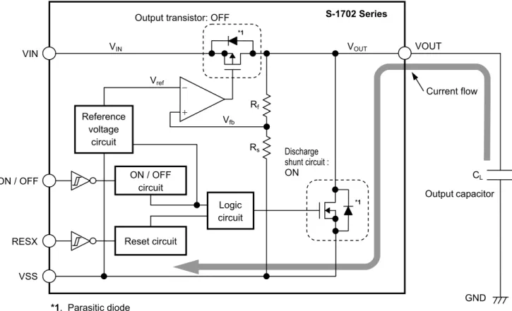
ON / OFF
VSS
Output transistor: OFF
Discharge shunt circuit : ON VOUT *1. Parasitic diode Current flow GND Output capacitor S-1702 Series RESX *1 VIN VOUT − + ON / OFF circuit VIN *1 Logic circuit Reset circuit Reference voltage circuit CL Vref Vfb Rs Rf
3. Detector block
3. 1 Basic operationFigure 28 shows a block diagram of the detector block.
Rc Rb Delay circuit VDOUT VIN Current supply Vref VDOUT + − VIN CD SENSE VSENSE Output circuit Ra VSS VSS VSS N1 CD
Figure 28 Block Diagram (Detector Block)
(1) When the SENSE voltage (VSENSE) is the release voltage (+VDET) or more, the VDOUT pin outputs “H”. ((1) in Figure 29)
In this case, the transistor (N1) is off and the input voltage to the comparator is (Rb+ Rc) • VSENSE Ra+ Rb+ Rc
.
(2) Although the SENSE voltage (VSENSE) drops to the release voltage (+VDET) or less, the VDOUT pin outputs “H” when the SENSE voltage (VSENSE) is the detection voltage (−VDET) or more.
If the SENSE voltage (VSENSE) is the detection voltage (−VDET) or less (refer to point A in Figure 29), the VDOUT pin outputs “L” ((2) in Figure 29).
The transistor (N1) is turned on and the input voltage to the comparator is Rb• VSENSE Ra+ Rb
.
(3) If the VIN input voltage (VIN) further drops to the lowest operating voltage of the S-1702 Series, the VDOUT pin is sets in high impedance.
If the VDOUT pin is pulled up to the regulator output voltage (VOUT), the VDOUT pin outputs VOUT (“H”) ((3)
in Figure 29).
(4) If the VIN input voltage (VIN) rises to the lowest operating voltage or more, the VDOUT pin outputs “L”. Although the SENSE voltage (VSENSE) excceds the detection voltage (−VDET), it is the release voltage (+VDET) or less, the VDOUT pin outputs “L” ((4) in Figure 29).
(5) If the SENSE voltage (VSENSE) rises to the release voltage (+VDET) or more (see point B in Figure 29), the VDOUT pin outputs “H”. The VDOUT pin outputs “H” after it is delayed for tD by the delay circuit ((5) in
Figure 29).
In the S-1702 Series, the detection voltage (VDOUT) can be set within the range of 1.3 V to 5.2 V (operating voltage range: VIN = 0.8 V to 6.5 V).
A
B
VDD
tD
VSS
Lowest operating voltage
VDOUT VSENSE (VIN)*1
VSS
(1)
Hysteresis width (VHYS) Release voltage (+VDET)
Detection voltage (–VDET)
*1. When the SENSE pin is connected to the VIN pin. (2) (3) (4) (5)
Figure 29 Operation
3. 1. 1 Regulator output voltage (VOUT) detection types (S-1702Axx, Bxx, Cxx, Dxx, Lxx, Mxx)
Each detector block of S-1702Axx, Bxx, Cxx, Dxx, Lxx, and Mxx detects the regulator output voltage (VOUT).
Rc Rb Delay circuit VDOUT VIN Current supply Vref VDOUT + − VIN CD *1 VOUT Output circuit Ra VSS N1 CD VSS VSS *1. S-1702Lxx and S-1702Mxx only
Figure 30 Block Diagram (Regulator Output Voltage (VOUT) Detection Type)
Caution If the input voltage or load current changes transiently, undershoot or overshoot occurs in
the regulator output voltage (VOUT). In the product types that the regulator output voltage is
detected by the detector, if the output voltage reaches the detection voltage or less due to undershoot, the detector operates so that a reset signal may be output. To prevent this, set the value of the capacitor so that the value of undershoot is the minimum, or set the voltage range in which the difference of the output voltage and the detection voltage is undershoot or more.
3. 1. 2 Input voltage (VIN) detection types (S-1702Exx, Fxx, Gxx, Hxx, Nxx, Pxx)
Each detector block of S-1702Exx, Fxx, Gxx, Hxx, Nxx, and Pxx detects the input voltage (VIN).
Rc Rb Delay circuit VDOUT VIN Current supply Vref VDOUT + − VIN Output circuit Ra VSS N1 CD VSS VSS *1. S-1702Nxx and S-1702Pxx only CD *1
Figure 31 Block Diagram (Input Voltage (VIN) Detection Type)
3. 1. 3 SENSE voltage (VSENSE) detection types (S-1702Jxx, Kxx)
Each detector block of S-1702Jxx and Kxx detects the SENSE voltage (VSENSE).
Rc Rb Delay circuit VDOUT VIN Current supply Vref VDOUT + − VIN SENSE VSENSE Output circuit Ra N1 VSS VSS
Figure 32 Block Diagram (SENSE Voltage (VSENSE) Detection Type)
Caution Use the SENSE pin as an input pin when detecting the external power supply voltage. If
applying an input voltage (VIN) while a potential is being applied to the SENSE pin, an error
occurs in the release voltage of the detector. Apply a voltage to the SENSE pin after applying
3. 2 Delay circuit
3. 2. 1 Internal delay types (S-1702Axx, Bxx, Cxx, Dxx, Exx, Fxx, Gxx, Hxx, Jxx, Kxx)
In the internal delay types, when VSENSE is turned on, the delay circuit makes a certain delay, after the point when VSENSE has reached the release voltage (+VDET), and sets the VDOUT pin to output an output signal (refer to point B in Figure 29). The delay circuit does not make delay when VSENSE is the detection voltage (−VDET) or less (refer to point A in Figure 29).
The delay time (tD) is fixed in the internal circuit of internal delay types. 3. 2. 2 External delay types (S-1702Lxx, Mxx, Nxx, Pxx)
In the external delay types, the delay time of the detection signal can be set by connecting a capacitor (CD) between the CD and VSS pins.
The delay time (tD) is determined according to the built-in constant current, approx. 100 nA (typ.), and the time constant of the external capacitor (CD), and can be calculated by the following equation.
tD [ms] = Delay constant × CD [nF] The delay constant (Ta = +25°C) is as follows.
Delay constant: 5.3 (min.), 6.3 (typ.), 7.3 (max.)
Figure 33 shows the equivalent circuit of the CD pin (external delay type).
VSS CD VSS VIN VIN CD VSS
Figure 33 Equivalent Circuit of CD Pin (External Delay Type)
Caution 1. Design the board so that a current will not flow into or flow out from the CD (RESX) pin, because this pin’s impedance is high. (Otherwise that may provide incorrect delay time.)
2. There is no limit for the capacitance of the external capacitor (CD) as long as the leakage
current of the capacitor can be ignored against the built-in constant current value. Leakage current causes deviation in delay time. When the leakage current is the built-in constant current or more, the IC does not release.
3. 3 Output Circuit
Either Nch open drain output, CMOS output (VOUT drive), or CMOS output (VIN drive) is used for the VDOUT pin. For details, refer to “Table 2 Output Types of VDOUT Pin”.The equivalent circuits are shown below.
VDOUT
VSS VSS
VDOUT
Nch open drain output
*1
VOUT
VSSVSS
VDOUT VDOUT
CMOS output (VOUT drive)
*1
VIN
VSS VSS
VDOUT VDOUT
CMOS output (VIN drive) *1. Parasitic diode
4. Relation of temperature coefficients of detector and regulator blocks
The S-1702 Series has a detector and a regulator in it, and each reference voltage circuit has the same structure so that both temperature coefficients of detector detection voltage and regulator output interlock.
4. 1 Positive temperature coefficient of regulator output
If the temperature coefficient of regulator output is positive, so is that of detector detection voltage (Figure 35).
85 Temperature gradient of detector
Ta [°C] 25
−40
−VDET [V]
Temperature gradient of regulator
Figure 35 Relation of Temperature Coefficients of Detector and Regulator (When They Are Positive)
4. 2 Negative temperature coefficient of regulator output
If the temperature coefficient of regulator output is negative, so is that of detector detection voltage (Figure 36).
85 Ta [°C]
25
−40
−VDET [V] Temperature gradient of detector
Temperature gradient of regulator
Precautions
• Wiring patterns for the VIN, VOUT and GND pins should be designed so that the impedance is low. When mounting an output capacitor between the VOUT and VSS pins (CL) and a capacitor for stabilizing the input between the VIN and VSS pins (CIN), the distance from the capacitors to these pins should be as short as possible.
• Note that the output voltage may increase when a series regulator is used at low load current (1.0 mA or less).
• Generally a series regulator may cause oscillation depending on the selection of external parts. The following conditions are recommended for this IC. However, be sure to perform sufficient evaluation under the actual usage conditions for selection, including evaluation of temperature characteristics.
Input capacitor (CIN): 1.0 μF or more Output capacitor (CL): 1.0 μF or more Equivalent series resistance (ESR): 10 Ω or less
• The voltage regulator may oscillate when the impedance of the power supply is high and the input capacitor is small or an input capacitor is not connected.
• The application conditions for the input voltage, output voltage, and load current should not exceed the package power dissipation.
• Do not apply an electrostatic discharge to this IC that exceeds the performance ratings of the built-in electrostatic protection circuit.
• In determining the output current, attention should be paid to the output current value specified in Table 7 of “
Electrical Characteristics” and footnote *8 of the table.
• SII claims no responsibility for any disputes arising out of or in connection with any infringement by products including this IC of patents owned by a third party.
Characteristics (Typical Data)
1. Entire circuit
Current consumption during operation*1 vs. Input voltage (Ta = +25°C)
VOUT = 1.5 V VOUT = 3.1 V 0 2 5 6 7 I SS [ μ A] 10 8 0 VIN [V] 1 3 4 12 6 4 2 Ta = 85°C Ta = 25°C Ta = −40°C 0 2 5 6 7 I SS [ μ A] 10 8 0 VIN [V] 1 3 4 12 6 4 2 Ta = 85°C Ta = 25°C Ta = −40°C VOUT = 5.5 V 0 2 5 6 7 I SS [ μ A] 10 8 0 VIN [V] 1 3 4 12 6 4 2 Ta = 85°C Ta = 25°C Ta = −40°C
2. Regulator block
2. 1 Output voltage vs. Output current (when load current increases) (Ta = +25°C)
VOUT = 1.5 V VOUT = 3.1 V 0 100 200 450 V OUT [V] 3.0 1.0 0 IOUT [mA] 300 4.0 2.0 350 400 250 150 50 VIN = 3.4 V VIN = 4.0 V VIN = 5.0 V VIN = 6.5 V 3.5 2.5 1.5 0.5 VOUT = 5.5 V 0 100 200 450 V OUT [V] 5 3 1 0 IOUT [mA] 6 300 4 2 350 400 250 150 50 VIN = 5.8 V VIN = 6.0 V VIN = 6.5 V
Remark In determining the output current,
attention should be paid to the followings. (1) The minimum output current value and
footnote *8 in Table 7 of “Electrical
Characteristics”.
(2) Power dissipation of package
2. 2 Output voltage vs. Input voltage (Ta = +25°C)
VOUT = 1.5 V VOUT = 3.1 V 1.0 1.5 2.0 2.5 3.0 V OUT [V] 1.6 1.5 1.4 1.3 1.2 1.1 1.0 VIN [V] 3.5 IOUT = −1 mA IOUT = −30 mA IOUT = −100 mA VOUT [V] 3.2 3.0 2.9 2.8 2.7 2.6 2.5 IOUT = −1 mA IOUT = −30 mA IOUT = −100 mA 2.5 3.0 3.4 4.0 4.5 VIN [V] 5.0 3.1 VOUT = 5.5 V 4.5 5.0 5.5 6.0 V OUT [V] 5.6 5.3 5.1 5.0 4.8 4.7 4.5 VIN [V] 6.5 4.6 4.9 5.2 5.4 5.5 IOUT = −1 mA IOUT = −30 mA IOUT = −100 mA
2. 3 Dropout voltage vs. Output current VOUT = 1.5 V VOUT = 3.1 V 0 75 150 V drop [V] 0.5 0.4 0.3 0.2 0.1 0 IOUT [mA] 100 50 Ta = 85°C Ta = 25°C Ta = −40°C 125 25 0 75 150 V drop [V] 0.30 0.25 0.15 0.10 0.05 0 IOUT [mA] 100 50 125 25 0.20 Ta = 85°C Ta = 25°C Ta = −40°C VOUT = 5.5 V 0 75 150 V drop [V] 0.25 0.15 0.10 0.05 0 IOUT [mA] 100 50 125 25 0.20 Ta = 85°C Ta = 25°C Ta = −40°C
2. 4 Output voltage vs. Ambient temperature
VOUT = 1.5 V VOUT = 3.1 V −40 0 25 50 75 V OUT [V] 1.50 1.30 1.20 1.10 Ta [°C] 1.40 −25 85 1.45 1.35 1.25 1.15 −40 0 25 50 75 V OUT [V] 3.30 3.10 3.00 2.90 Ta [°C] 3.20 −25 85 3.25 3.15 3.05 2.95 VOUT = 5.5 V −40 0 25 50 75 V OUT [V] 5.70 5.50 5.40 5.30 Ta [°C] 5.60 −25 85 5.65 5.55 5.45 5.35
2. 5 Current consumption during operation at regulator block*1 vs. Input voltage VOUT = 1.5 V VOUT = 3.1 V 0 2 5 6 7 I SS1 [ μ A] 8 0 VIN [V] 1 3 4 10 6 4 2 Ta = 85°C Ta = 25°C Ta = −40°C 0 2 5 6 7 I SS1 [ μ A] 8 0 VIN [V] 1 3 4 10 6 4 2 Ta = 85°C Ta = 25°C Ta = −40°C VOUT = 5.5 V 0 2 5 6 7 I SS1 [ μ A] 8 0 VIN [V] 1 3 4 10 6 4 2 Ta = 85Ta = 25°°CC Ta = −40°C
*1. Excluding current flowing in pull-up and pull-down resistors connected to the ON / OFF or RESX pins
2. 6 Ripple rejection ratio (Ta = +25°C)
VOUT = 1.5 V, VIN = 2.5 V, CL = 1.0 μF VOUT = 3.1 V, VIN = 4.1 V, CL = 1.0 μF 10 100 1k 10k 100k Ripple Rejection [dB] 0 20 40 60 80 Frequency [Hz] 1M 100 IOUT = 1 mA IOUT = 30 mA IOUT = 150 mA 10 100 1k 10k 100k Ripple Rejection [dB] 0 20 40 60 80 Frequency [Hz] 1M 100 IOUT = 1 mA IOUT = 30 mA IOUT = 150 mA VOUT = 5.5 V, VIN = 6.0 V, CL = 1.0 μF 10 100 1k 10k 100k Ripple Rejection [dB] 0 20 40 60 80 Frequency [Hz] 1M 100 IOUT = 1 mA IOUT = 30 mA IOUT = 150 mA
3. Detector block
3. 1 Detection voltage vs. Ambient temperature
−VDET = 1.3 V −VDET = 2.75 V −40 0 25 50 75 Detection Voltage [V] 1.50 1.30 1.20 1.10 Ta [°C] 1.40 −25 85 1.45 1.35 1.25 1.15 −VDET +VDET −40 0 25 50 75 Detection Voltage [V] 3.0 2.7 2.6 2.4 Ta [°C] 2.9 −25 85 2.8 2.5 −VDET +VDET −VDET = 5.2 V −40 0 25 50 75 Detection Voltage [V] 5.5 5.0 Ta [°C] −25 85 5.4 5.3 5.2 5.1 −VDET +VDET
3. 2 Hysteresis width vs. Ambient temperature
−VDET = 1.3 V −VDET = 2.75 V −40 0 25 50 75 Hysteresis [%] 6 3 2 0 Ta [°C] 5 −25 85 4 1 S-1702xAx, xBx, xCx S-1702xDx, xEx, xFx S-1702xGx, xHx, xJx −40 0 25 50 75 Hysteresis [%] 6 3 2 0 Ta [°C] 5 −25 85 4 1 S-1702xAx, xBx, xCx S-1702xDx, xEx, xFx S-1702xGx, xHx, xJx −VDET = 5.2 V −40 0 25 50 75 Hysteresis [%] 6 3 2 0 Ta [°C] 5 −25 85 4 1 S-1702xAx, xBx, xCx S-1702xDx, xEx, xFx S-1702xGx, xHx, xJx
3. 3 Current consumption during operation at detector block*1 vs. Input voltage −VDET = 1.3 V −VDET = 2.75 V 0 2 5 6 6.5 I SS2 [ μ A] 2.52.0 0 VIN [V] 1 3 4 3.5 1.5 1.0 0.5 3.0 Ta = 85°C Ta = 25°C Ta = −40°C 0 2 5 6 6.5 I SS2 [ μ A] 2.52.0 0 VIN [V] 1 3 4 3.5 1.5 1.0 0.5 Ta = 85°C Ta = 25°C Ta = −40°C 3.0 −VDET = 5.2 V 0 2 5 6 6.5 I SS2 [ μ A] 2.52.0 0 VIN [V] 1 3 4 3.5 1.5 1.0 0.5 Ta = 85°C Ta = 25°C Ta = −40°C 3.0
*1. Excluding current flowing in pull-up and pull-down resistors connected to the ON / OFF or RESX pins 3. 4 Detector output voltage vs. Nch transistor
characteristics (ID vs. VDS characteristics)
3. 5 Detector output voltage vs. Pch transistor
characteristics (ID vs. VDS characteristics) (Ta = +25°C) (Ta = +25°C) 0 2 4 5 6 I D [mA] 20 15 0 VDS [V] 1 3 30 10 5 25 VIN = 4.0 V VIN = 3.0 V VIN = 2.0 V VIN = 1.3 V VIN = 5.0 V 0 2 4 5 6 I D [mA] 20 15 0 VDS [V] 1 3 30 10 5 25 VIN = 4.0 V VIN = 3.0 V VIN = 2.0 V VIN = 1.5 V VIN = 5.0 V
3. 6 Detector output voltage vs. Input voltage
CMOS output Nch open drain output
0 0.4 1.0 1.2 1.4 V DOUT [V] 5 4 0 VIN [V] 0.2 0.6 0.8 6 3 2 1 Ta = 85°C Ta = 25°C Ta = −40°C 0 0.4 1.0 1.2 1.4 V DOUT [V] 0.5 0.4 0 VIN [V] 0.2 0.6 0.8 0.6 0.3 0.2 0.1 Ta = 85°C Ta = 25°C Ta = −40°C
Reference Data
1. Input transient response characteristics (Ta =
+
25°C)
IOUT = 30 mA, tr = tf = 5.0 μs, CL = 1.0 μF, CIN = 1.0 μF VOUT = 1.5 V, VIN = 2.5 V ↔ 3.5 V IOUT = 30 mA, tr = tf = 5.0 μs, CL = 1.0 μF, CIN = 1.0 μF VOUT = 3.1 V, VIN = 4.1 V ↔ 5.1 V V OUT [V] 1.60 1.58 1.56 1.54 1.52 1.50 1.48 1.46 1.44 t [μs] V IN [V] 4.0 3.0 2.5 2.0 0 0.5 1.0 1.5 3.5 −50 0 50 100 150 200250 300350 −100 VOUT VIN V OUT [V] 3.35 3.30 3.25 3.20 3.15 3.10 3.05 3.00 2.95 t [μs] V IN [V] 5.5 4.5 4.0 3.5 1.5 2.0 2.5 3.0 5.0 −50 0 50 100 150 200 250300350 −100 VOUT VIN2. Load transient response characteristics (Ta =
+
25°C)
VIN = 2.5 V, CL = 1.0 μF, CIN = 1.0 μF VOUT = 1.5 V, IOUT = 50 mA ↔ 100 mA VIN = 4.0 V, CL = 1.0 μF, CIN = 1.0 μF VOUT = 3.1 V, IOUT = 50 mA ↔ 100 mA V OUT [V] 1.70 1.65 1.60 1.55 1.50 1.45 1.40 1.35 t [μs] I OUT [mA] 150 50 0 −200 −150 −100 −50 100 −50 0 50 100 150 200250 300350 −100 VOUT IOUT V OUT [V] 3.30 3.25 3.20 3.15 3.10 3.05 3.00 2.95 t [μs] I OUT [mA] 150 50 0 −50 −200 −150 −100 100 −50 0 50 100 150 200 250300350 −100 VOUT IOUT VIN = 6.0 V, CL = 1.0 μF, CIN = 1.0 μF VOUT = 5.5 V, IOUT = 50 mA ↔ 100 mA V OUT [V] 6.40 6.20 6.00 5.80 5.60 5.40 5.20 5.00 t [μs] I OUT [mA] 150 50 0 −50 −200 −150 −100 100 −50 0 50 100 150 200250 300350 −100 VOUT IOUT3. ON/OFF pin transient response characteristics (Ta =
+
25°C)
VIN = 2.5 V, CL = 1.0 μF, CIN = 1.0 μF, IOUT = 100 mA VOUT = 1.5 V, VON / OFF = 0 V → 2.5 V VIN = 4.0 V, CL = 1.0 μF, CIN = 1.0 μF, IOUT = 100 mA VOUT = 3.1 V, VON / OFF = 0 V → 4.0 V V OUT [V] 5.0 4.0 3.0 2.0 1.0 0 −1.0 t [μs] V ON / OFF [V] 3.0 1.0 0 −3.0 −2.0 −1.0 2.0 300 400 0 100 200 500 −100 VOUT VIN V OUT [V] 10.0 8.0 6.0 4.0 2.0 0 −2.0 t [μs] V ON / OFF [V] 6.0 2.0 0 −6.0 −4.0 −2.0 4.0 300 400 0 100 200 500 −100 VOUT VIN VIN = 6.0 V, CL = 1.0 μF, CIN = 1.0 μF, IOUT = 100 mA VOUT = 5.5 V, VON / OFF = 0 V → 6.5 V V OUT [V] 14.0 12.0 8.0 6.0 4.0 0 −2.0 t [μs] V ON / OFF [V] 8.0 2.0 0 −8.0 −6.0 −2.0 4.0 300 400 0 100 200 500 −100 VOUT VIN 6.0 −4.0 2.0 10.0No. TITLE SCALE UNIT mm
SNT-6A-A-PKG Dimensions
PG006-A-P-SD-2.0
No. PG006-A-P-SD-2.0
0.2±0.05 0.48±0.02 0.08+0.05-0.02 0.5 1 2 3Feed direction 4.0±0.1 ø0.5 1.85±0.05 0.65±0.05 5° No. TITLE SCALE UNIT mm
PG006-A-C-SD-1.0
SNT-6A-A-Carrier Tape
No. PG006-A-C-SD-1.0
+0.1 -0 1 2 4 3 5 69.0±0.3 ø13±0.2 (60°) (60°) QTY.
No. PG006-A-R-SD-1.0
PG006-A-R-SD-1.0
Enlarged drawing in the central part
No. TITLE SCALE UNIT mm
SNT-6A-A-Reel
5,000No. TITLE SCALE UNIT mm SNT-6A-A-Land Recommendation
PG006-A-L-SD-4.0
No. PG006-A-L-SD-4.0
0.3 0.2 1.36 0.52 1 2Caution 1. Do not do silkscreen printing and solder printing under the mold resin of the package. 2. The thickness of the solder resist on the wire pattern under the package should be 0.03 mm
or less from the land pattern surface.
3. Match the mask aperture size and aperture position with the land pattern. 4. Refer to "SNT Package User's Guide" for details.
1. (0.25 mm min. / 0.30 mm typ.)
2. (1.30 mm ~ 1.40 mm)
0.03 mm SNT
1. Pay attention to the land pattern width (0.25 mm min. / 0.30 mm typ.).
2. Do not widen the land pattern to the center of the package ( 1.30 mm ~ 1.40 mm ).
1. 2. ※1. 䇋⊼ᛣ⛞Ⲭᓣⱘᆑᑺ(0.25 mm min. / 0.30 mm typ.)DŽ ※2. 䇋࣓ᇕ㺙Ё䯈ᠽሩ⛞Ⲭᓣ (1.30 mm ~ 1.40 mm)DŽ ⊼ᛣ1. 䇋࣓ᷥ㛖ൟᇕ㺙ⱘϟ䴶ॄࠋϱ㔥ǃ⛞䫵DŽ 2. ᇕ㺙ϟǃᏗ㒓Ϟⱘ䰏⛞㝰८ᑺ (Ң⛞Ⲭᓣ㸼䴶䍋) 䇋ࠊ0.03 mmҹϟDŽ 3. 㝰ⱘᓔষሎᇌᓔষԡ㕂䇋Ϣ⛞Ⲭᓣᇍ唤DŽ 4. 䆺㒚ݙᆍ䇋খ䯙 "SNTᇕ㺙ⱘᑨ⫼ᣛफ"DŽ