The In
fl
uence of Microstructure and Grain Boundary
on the Electrical Properties of Scandia Stabilized Zirconia
Jingchao Tao, Anping Dong and J. Wang
+State Key Laboratory of Metal Matrix Composites, Shanghai Jiao Tong University, Shanghai 200240, P. R. China
Nanocrystalline Sc2O3(different doping content) stabilized ZrO2(ScSZ) powders are prepared by the hydrothermal method. Dense ScSZ ceramic pellets are fabricated by isostatically pressing then sintering at 1350°C for 2 h. 8 mol%Sc2O3doped Zirconia possesses the highest conductivity of all the samples measured by impedance spectroscopy. Different grain size of 8ScSZ samples which are observed by scanning electron microscopy (SEM) are prepared by sintering with different temperature and different hours. The correlation between grain size and electrical properties is analyzed by impedance spectroscopyfitting and calculating with brick-layer model and MottShottky model: the total grain boundary conductivity decreases but the specific grain boundary conductivity increases with the decrease in grain size of 8ScSZ; the grain boundary space charge potential decreases and the concentration of oxygen vacancies in the space charge regions increases with decreasing grain size. [doi:10.2320/matertrans.M2012385]
(Received November 19, 2012; Accepted February 13, 2013; Published April 5, 2013)
Keywords: scandia stabilized zirconia, oxygen vacancy, specific grain boundary conductivity, space charge potential
1. Introduction
The cubic fluorite rare-earth doped ZrO2 materials are well-known candidates for the electrolyte of solid oxide fuel cell (SOFC) due to their high ionic conductivity, stability in both oxidizing and reducing environment and stability against the electrode materials.15) Of all known rare-earth doped ZrO2, Sc2O3 stabilized ZrO2 (hereinafter describe ScSZ) close to 8 mol% Sc2O3 content, has been shown to possess the highest oxygen ion mobility at elevated temper-atures (0.32 S cm¹1 at 1000°C).6,7) Thus the high ionic conductivity property of ScSZ has been extensively studied. The crystal structure of ScSZ is the foundation for conductivity. Undoped ZrO2 is monoclinic at room temper-ature (space group P21/c8,9)); with the increase of temper-ature (at zero pressure) the material transforms to tetragonal (space groups P42/nmc) structure at 1400 K and then to a cubicfluorite structure (space groups Fm3m) at 2650 K.1013) The doping of rare-earth oxides like Sc2O3 could stabilize the high-temperature phase of ZrO2to the room temperature. Especially the cubic zirconia is typically a fast ion conductor due to its high diffusion coefficient of oxygen.14)Appropriate Sc2O3 doping contents could restore the cubic structure similar to that of ZrO2. But the excessive doping might decrease the ionic conductivity due to the increased association between oxygen vacancies and dopant cations to form complex defects of low mobility.15)
Grain boundary is another key factor on ionic conductivity of ScSZ. At specific grain boundaries, i.e., the interfaces between adjacent grains, the conductivity of doped ZrO2 materials is ³2 orders of magnitude lower than the conductivity of bulk;1622) this very low grain boundary conductivity is mainly attributed to the intergranular siliceous phases1620) and the space charge effect. According to the core-space charge layer model,23) a grain boundary is consisted of a grain boundary core (crystallographic mismatch zone) and two adjacent space charge layers. The
depletion of oxygen vacancies in the grain boundary space charge layer is mainly responsible for the low grain boundary conductivity without the effect of the siliceous phases. This was also proposed by Burggraaf et al.24) in 1982. More recently, Y2O3doped ZrO2with high purity was studied, and a Schottky barrier model25)was proposed.
In this work, ScSZ samples with different Sc2O3 dopant contents were investigated and among all samples, the 8 mol% Sc2O3 doped ZrO2 (hereby noted 8ScSZ) was sintered at the same temperature but different hours to achieve various grain size. In order to prepare high purity and weakly agglomerated samples (either of which may affect the sintering property and electrical property), the hydrothermal preparation method was applied to prepare the ScSZ powder. By comparing the impedance spectroscopy and X-ray spectroscopy of the ScSZ samples with the different dopant Sc2O3 ratio, one can establish the correlation between the ionic conductivity and the corresponding change in the microstructure of the ScSZ. The other objective of this work is to explore the grain-size-dependent specific grain boundary conductivity of ScSZ by analyzing the thickness and space charge potential of grain boundaries.
2. Experimental
2.1 Preparation
Nanocrystalline ScSZ powders were prepared by the hydrothermal urea homogeneous precipitation method. Stoichiometric solutions of ZrClO2, (A.R.; Sinopharm Chemical Reagent Company, China), ScCl3 (99.95% Sinopharm Chemical Reagent Company, China) and urea (AR; Sinopharm Chemical Reagent Company, China) in the molar ratio of Zr4+/Sc3+=95/5 (5 mol% Sc2O3 doped ZrO2, 5ScSZ), 92/8 (8 mol%Sc2O3doped ZrO2, 8ScSZ) and 90/10 (10 mol%Sc2O3doped ZrO2, 10ScSZ) were employed to prepare the stock solution (100 mL) with a cation concentration of 0.2 mol¹1 in a Teflon cup (100 mL). The cup was then transferred into a stainless steel autoclave and subjected to a hydrothermal treatment at 110°C for 6 h and
+Corresponding author, E-mail: junwang@sjtu.edu.cn
subsequently at 200°C for another 6 h under autogenous pressure in an electric oven. As the autoclave cooled down to room temperature naturally, the precipitated powders were
filtered, washed with deionized water and ethanol in a centrifuge, and dried in a vacuum oven at about 110°C. The as-prepared powders were pressed isostatically into pellets with a diameter of 1011 mm and thickness of 0.9 1.0 mm under a pressure of 20 MPa, followed by sintering under static air at 1350°C for 2 h. 8ScSZ powders were sintered at 1350°C for 2, 4 and 36 h, respectively to achieve various grain size samples. The density (shown in Tables 1 and 2) of sintered pellets was determined by Archemides method.
2.2 Microstructural characterization
The microstructure of nano-crystalline ScSZ powders was investigated by means of transmission electron microscopy TEM (JEM 2100, 200KV, JEOL, Japan) to verify its weakly agglomerated morphology. Phase analysis was performed by X-ray diffraction using a Phillips X’Pert Pro powder diffractometer (Cu KR, 45 kV, 40 mA). Rietveld refinement was used to analyze the phase composition by the software of highscore plus.
The grain size and the microstructure of the pellets were observed using scanning electron microscopy SEM (Carl Zeiss LEO 1550 VPfield emission, 3 kV excitation voltage). The transmission electron microscopy TEM (JEM 2100, 200KV, JEOL, Japan) was also used to observe the morphology of the grain boundaries of ScSZ. The TEM samples were prepared by standard methods, involving mechanical grinding to a thickness of about 0.1 mm, dimpling to about 10 µm, and then ion-beam milling to electron transparency.
2.3 Impedance spectroscopy
The conductivity of sintered pellets was measured by AC impedance spectroscopy in air from 300 to 900°C with samples equilibrated for 30 min at each temperature.
Impedance spectra were measured every 1020°C. The measurement sequence was repeated several times until the resistance at each temperature stabilized. Data were collected in the frequency range from 0.02 to 107Hz using a Solartron 1260 and voltage of 200 mV. Platinum ink (Engelhard 6082) was brushed onto both polished surfaces. The ink was applied to one side of the samples and sintered at 900°C for 2 h, this procedure was repeated for the other side. Four-wire (2 platinum wires each side) system measurement was applied in order to minimize the inductance in the measure-ment configuration.
Normally, three arcs in the complex impedance spectra (Fig. 1) are observed in the high-to-low frequency sequence, corresponding to the responses of the bulk, grain boundaries and electrodes, respectively. The resulting impedance spectra were analyzed in terms of an equivalent circuit model in which (depending on the temperature regime) distinct RQ
subcircuits were used to represent the bulk and grain boundary regions, where Ris an ideal resistor with ZR=R,
and Q is a constant phase element with ZQ=(Y(j½)n)¹1,
where j is imaginary unit,½is the frequency, andYandnare constants with 0<n<1. The capacitance, C, of an RQ
[image:2.595.331.518.71.385.2]circuit was obtained from the relationC=Y1/nR(1/n¹1). The average values of n obtained for bulk and grain boundary subcircuits were both close to 1 (typically ³0.95 and³0.9, respectively), as required for meaningfully determining the capacitance by this expression. The data analysis was performed using the software package Zview (Scribner Associates Inc., Southern Pines, NC).
Table 1 Dopant content of Sc2O3of ScSZ, relative density and activation energies for the bulk and grain boundary conductivities.
Sample Relative density (%)
Etotala
(eV)
Ebulka
(eV)
Egba
(eV)
5ScSZ 97.8 1.02 0.96 1.08
8ScSZ 97.6 1.25 1.70 1.44
10ScSZ (<550°C) 97.5 1.46
[image:2.595.47.295.94.169.2]10ScSZ (>550°C) 98.1 0.77
Table 2 Sintering condition (temperature and time), relative density, average grain size and activation energies for the total and specific grain boundary conductivities of 8ScSZ.
Sintering condition Relative density (%)
dg (nm)
Egba
(eV)
Esp,gba
(eV)
1350°C©2 h 97.6 1000 1.44 1.34
1350°C©4 h 97.7 2500 1.51 1.51
1350°C©36 h 98.1 4000 1.44 1.51
0 10 20 30
-Z
'' imag
K
Ω
Z'real KΩ
(a) 5ScSZ
340°C
10MHz
Electrode
Bulk
Grain Boundary
0 10 20 30 40 50
0 5 10 15 20
0 5 10 15
-Z
'' imag
K
Ω
Z'
real KΩ
(b)8ScSZ
[image:2.595.46.291.235.297.2]3. Results and Discussion
3.1 Microstructure analysis
3.1.1 Impact of Sc2O3 dopant content on ScSZ crystal
structure
In order to prepare high-purity ScSZ powders with well-controlled compositions and microstructure, the hydro-thermal homogeneous precipitation method has been em-ployed. This approach has additional advantages of avoiding unnecessary grain growth and aggregation each of which will severely affect the sintering density and electrical property. From the TEM image shown in Fig. 2, it was observed that the as-prepared 8ScSZ powders were an assembly of homogeneous and weakly agglomerated nano-crystals.
It is well known that undoped ZrO2 is in a monoclinic phase. Undoped ZrO2is difficult to densify by sintering due to the stress relaxation induced by phase transition. By doping Sc3+ whose ionic radius is smaller than Zr4+, the high-temperature phase could be stabilized down to room temperature. As shown in Fig. 3, different doping ratio results in different crystal structures: 5ScSZ and 8ScSZ are cubic phase, but 10ScSZ has mixed cubic and rhombohedral phases due to the decomposition of the cubic phase.
Whether ScSZ can achieve cubic phase is sensitive to the content of Sc2O3dopant. Only about 58 mol%Sc2O3dopant content could stabilize the cubic phase to room temperature. It is shown in Fig. 3 that cubic phase will decompose partially to the rhombohedral phase when the Sc2O3dopant content exceeds 8 mol%. According to eq. (1), the concen-tration of oxygen vacancy is a constant once the Sc2O3 dopant content is decided.
Sc2O3ZrO22Sc0Zrþ3OOþVO•• ð1Þ
Where ScAZrmeans that a Zr4+site is replaced by a Sc3+;OO
means that O2¹ is still on its original site; V••
O stands for
an oxygen vacancy. The concentration of oxygen vacancy increases with the increase of doping level of Sc2O3.
According to EinsteinNernst equation (eq. (2)), the con-ductivity of ScSZ sample is the function of the concentration of carrier (in this case the oxygen vacancy). Where ·iis the conductivity,ciis the concentration of carrier,ziis the charge of species, e is the electron charge, KB is Boltzmann’s constant. Therefore, the conductivity of ScSZ dependent on temperature (Fig. 4) is the function of the different Sc2O3 dopant content.26)
·i¼cizi2e2Di=KBT ð2Þ
As shown in Fig. 4, 10ScSZ has very low conductivity, which is even smaller than that of 5ScSZ whose concen-tration of oxygen vacancy is smaller than that of 10ScSZ under 550°C due to the appearance of the rhombohedral
Fig. 2 TEM image of 8ScSZ powder prepared by hydrothermal
precip-itation. 0
2500 5000 7500 0 2400 4800 7200 96000 1200 2400 3600 4800
80° 70°
60° 50°
40°
30°
2θ (a) 5ScSZ
20°
cubic
counts
(b) 8ScSZ (c) 10ScSZ
Rhombohedral
Fig. 3 X-ray diffraction patterns of 1350°C sintering 2 h ScSZ pellets with different doping ratio.
0.8 1.0 1.2 1.4
-4 -2 0 2 4
977 727 560 441
T(°C)
log
σ
T(
Ω
−1•
cm
-1•
K)
1000/T(1/K)
5ScSZ 8ScSZ 10ScSZ
[image:3.595.54.286.67.293.2] [image:3.595.323.533.68.326.2] [image:3.595.319.536.376.566.2]phase.27)Meanwhile as shown in Table 1, 10ScSZ has higher activation energy of 1.46 eV than that of 5ScSZ of 1.02 eV and 8ScSZ of 1.25 eV. The data of activation energy show that conductivity of 10ScSZ has the tendency to be higher than that of both 5ScSZ and 8ScSZ at high temperature. However, the conductivity of 10ScSZ becomes much higher which is similar to 8ScSZ when the temperature is beyond 550°C. The activation energy of 8ScSZ and 10ScSZ beyond 550°C becomes similar, too. (Table 1) All the activation energies could be calculated by Arrhenius equation (eq. (3)). WhereEais the activation energy,Ais pre-exponential factor determined from afit of the data to the equation,TandKBare temperature and Boltzmann constant, respectively.
·T ¼AexpðEa=KBTÞ ð3Þ
Such facts suggest that a phase transition exists between 550 and 600°C, which is verified by high-temperature X-ray diffractometry. As shown in Fig. 5, 10ScSZ is in the rhombohedral phase from room temperature up to 550°C but it transforms to a cubic phase at 600°C and stays in this phase up to 1000°C. This is in agreement with the phase diagram of the Sc2O3ZrO2system.28)
3.1.2 Impact of Sc2O3dopant content on grain size and
conductivity
The doping level of Sc2O3 affects both crystal structure and grain size of ScSZ. As shown in Fig. 6, with the increase of Sc2O3content, the grain size of sintered ScSZ pellets also increases. The grain size of 5ScSZ and 8ScSZ is about 200 and 1000 nm, respectively. The size of the majority of 10ScSZ grains is about 1000 nm, but a small portion is at about 200 nm resulting from the rhombohedral crystal structure decomposed from the cubic phase. Macroscopically, the grain boundary density of one ScSZ sample will decrease due to the increase of the grain size. The decrease of grain boundary density contributes to the decrease of the total grain
boundary resistance.29) The conductivity of both bulk and total grain boundary of 5ScSZ and 8ScSZ are presented in Figs. 7(a) and 7(b), respectively. Because of the frequency limitation of conventional impedance meters, it is impossible to measure the grain interior and grain boundary conductiv-ities at high temperatures independently. However, one can extrapolate both bulk and grain boundary conductivities at high temperature with an Arrhenius equation, specifically (eq. (3)).
As a result the conductivity of total grain boundary of 8ScSZ is greater than that of the bulk below 420°C but while it’s smaller than that of the bulk above this temperature (Fig. 7(b)) because the activation energy of bulk which is 1.70 eV is higher than that of the grain boundary which is 1.44 eV shown in Table 1. But in the case of 5ScSZ, which
0 1200 2400 3600 48000 1100 2200 3300 44000 1300 2600 3900 52000 1500 3000 4500 60000 1500 3000 4500 6000
40° 35°
30°
25° 2θ
room temperature 550°C
rhombohedral
counts
600°C
cubic
700°C 1000°C
Fig. 5 High temperature X-ray diffraction patterns of 10ScSZ.
(a)
(b)
(c)
[image:4.595.312.540.68.555.2] [image:4.595.65.274.69.330.2]has a smaller grain size than 8ScSZ (Fig. 6), the higher density of grain boundaries leads to a smaller conductivity of grain boundaries than that of bulk below 450°C, but a higher grain-boundary conductivity than that of bulk (Fig. 7(a)) above this temperature because the activation energy of total grain boundary which is 1.08 eV is higher than that of the bulk which is 0.96 eV shown in Table 1. Therefore lowering grain boundary density (preparation of columnar crystal or single crystal) of 8ScSZ material used as electrolyte at the working temperature (normally 6001000°C) is vital to future research (This is beyond the scope of the present work).
3.2 Impact of grain size of ScSZ on specific grain boundary conductivity
3.2.1 Brick layer model and specific grain boundary conductivity
The grain size of 8ScSZ pellets increases with extended sintering time (Fig. 8). The grain size of 8ScSZ sintered for 36 h is almost 4000 nm which is 4 times of the sample sintered for 2 h. The growth of the grain size results in the decrease of the total amount of grain boundaries which contributes markedly to the higher conductivity of total grain boundary (Fig. 9(a)).
The total grain boundary conductivity is a convolution of conductance across a single grain boundary and the number of grain boundaries within the sample. It is relatively common practice to extract from the impedance data the specific grain boundary conductivity (a real material property independent of microstructure) by making use of the “brick layer” model.30) While that model is constructed for a particular microstructural configuration (cube-shaped grains aligned with the direction of currentflow), similar results can be derived for any arbitrary geometry. Specifically, ignoring grain boundaries parallel to the direction of currentflow, the total grain boundary resistance, Rtotalgb , of a polycrystalline
material is given by eq. (4).
-6 -5 -4 -3 -2 -1 0
T(°C)
log
σ
T(
Ω
−1 •
cm
-1 •
K)
1000/T(1/K) σbulk
σgb
(a)
-3.0 -2.5 -2.0 -1.5 -1.0 -0.5 0.0
1.3 1.4 1.5 1.6 1.7 1.8 1.9 2.0
496 441 394 352 315 283 253 227
1.40 1.45 1.50 1.55 1.60 1.65 1.70
441 417 394 372 352 333 315
T(°C)
log
σ
T(
Ω
−1•
cm
-1•
K)
1000/T(1/K) σbulk
σgb
(b)
Fig. 7 Temperature dependences of bulk and grain boundary conductivities for (a) 5ScSZ and (b) 8ScSZ.
(a)
(b)
(c)
[image:5.595.312.542.68.563.2] [image:5.595.65.275.75.445.2]Rtotalgb ¼NRspgb ¼NμspgbA¤ ð4Þ
Where μ is resistivity, ¤ is the thickness of single grain boundary, A is area and N is the number of single grain boundary and subscripts “gb” and “sp” indicate grain boundary and specific, respectively. Similarly, the capaci-tance of bulk and grain boundary is given by eqs. (5) and (6), respectively,
Cbulk¼¾0¾bulk A
Lbulk ð5Þ
Cgb¼¾0¾gb A
Lgb ð6Þ
where ¾0 is the permittivity of a vacuum, ¾ is the relative dielectric constant, and L is the length. For a material with moderate grain sizeLbulk³Lsample,Agb³Abulk³Asampleand
Lgbis the product of the grain boundary thickness,¤, and the number of grain boundary,N. It is reasonable for¾gb³¾bulk because the bulk and grain boundary regions are similar in both chemistry and atomic arrangement. The quantity
Lsample/N is the distance between 2 grain boundaries which is equivalent to the grain size of the brick layer model, dg. Equations (7) and (8) could be obtained by using these approximations.
Cbulk
Cgb ¼
¤N Lsample ¼
¤
dg ð7Þ 1
·total gb
¼ 1
·spgb
¤N
Lsample ð8Þ
Combining eqs. (7) and (8) by using the substitution with ·=1/μand·=L/AR, one obtains eq. (9).
·spgb¼C bulk
Cgb · total
gb ð9Þ
Specific grain boundary conductivity of ScSZ could be calculated from this analysis in which the capacitance of both bulk and grain boundary can befitted from Fig. 10 and the total grain boundary conductivity is shown in Fig. 9(a). As a result the conductivity of specific grain boundary of 8ScSZ is plotted in the Arrhenius form as a function of temperature. As is shown in Fig. 9(b), the conductivity of specific grain boundary of 8ScSZ decreases with the increase of grain size. The result is opposite of the case of total grain boundary of the same material. As shown in Table 2, both the activation energies of total grain boundary conductivity and specific conductivity of 8ScSZ with different grain size are similar.
3.2.2 Space charge potential
The“real”electrical property and specific grain boundary conductivity of 8ScSZ is affected by the purity and the space charge potential of the grain boundary. Transmission electron micrograph of 8ScSZ sintered at 1350°C for 2 h is presented in Fig. 11. This micrograph, which is representative of the overall microstructure, demonstrates that the grain bounda-ries are free of siliceous phase and any other amorphous phases. The grain boundaries were also studied by the energy-dispersive X-ray spectroscopy (EDXS). The different contents of Si and Sc of 8ScSZ at triple grain boundary, grain boundary and grain interior, respectively, were shown in Table 3. As a result, there is no Si or Sc segregation at grain boundaries.
According to the constancy of the electrochemical potential for mobile defects, the concentration C(x) of any dilute defect i with chargeZ in the space charge layer is
-2.5 -2.0 -1.5 -1.0 -0.5 0.0 0.5
log
σgb
T(
Ω
−1•
cm
-1•
K)
1000/T(1/K)
1000nm 2500nm 4000nm (a)
1.35 1.40 1.45 1.50 1.55 1.60 1.65 1.70
1.35 1.40 1.45 1.50 1.55 1.60 1.65 1.70
-6.0 -5.5 -5.0 -4.5 -4.0 -3.5 -3.0
log
σ
spT(gb
Ω
−1•
cm
-1•
K)
1000/T(1/K)
1000nm 2500nm 4000nm (b)
Fig. 9 Conductivity of (a) total grain boundary and (b) specific grain boundary of 8ScSZ pellets sintered in different condition with different grain size.
20 10
0 0 2 4 6 8 10 12 14
1000nm 2500nm 4000nm
-Z
'' imag
K
Ω
Z'
real KΩ
[image:6.595.61.276.67.415.2]350°C
[image:6.595.319.534.67.244.2]½CðxÞ
½CðbulkÞ¼exp
eZi¤ðxÞ
KBT
ð10Þ
wherexis the distance from the interface between the grain boundary core and the space charge layer, C is the concentration of oxygen vacancies, Z is 2 and eis electron charge.
Compared with the bulk, an ideal space charge layer would have a different composition, but with the same crystal structure, and a similar conduction mechanism, so the mobility of oxygen vacancies can be assumed to be equal for the bulk and space charge layer.23,31)Thus from eq. (10) the grain boundary resistance follows that
Rspgb
Rbulk¼
·bulk
·spgb ¼ 1
s
Zs
0
exp eZi¤ðxÞ
KBT
dx ð11Þ
wheresis the length of space charge layer and¦¤(x) is the electrostatic potential referenced to the bulk which follows that
¤ðxÞ ¼¤ð0Þ x s
s
2
ð12Þ
Combining eqs. (11) and (12) the grain boundary space charge potential ¦¤(0) is related to the specific grain boundary conductivity ·spgb and the bulk conductivity ·bulk
by eq. (13)
·bulk
·spgb ¼
exp½2e¤ð0Þ=KBT
4e¤ð0Þ=KBT ð13Þ
¦¤(0) can be calculated from·bulkwhich could befitted from
the impedance spectroscopy and·spgbvalues given in Fig. 9(b) at different temperature; results are presented in Fig. 12: the space charge potentials of 8ScSZ increases with the rise of temperature and enlargement of the grain size. The space charge potential of the sample of 8ScSZ with the grain size of 2500 nm is slightly higher than that of the sample with the grain size of 1000 nm. But the space charge potential of the sample of 8ScSZ with the grain size of 4000 nm is much higher than those of the samples with the grain size of 1000 and 2500 nm. It suggests that the tendency of the increase of the space charge potential is not linear with the increase of grain size of 8ScSZ.
To keep the equilibrium of the concentration of oxygen vacancies and the concentration of O2¹ on the surface and space charge layer of 8ScSZ the positive oxygen vacancies are depleted in this region due to the lack of negative charges. The depletion which was proposed as the cause of the
“intrinsic” grain boundary effect23,25) is described by combining eqs. (10) and (12) as eq. (14).
½V••
OðxÞ
½V••
OðbulkÞ¼
exp 2e¤ð0Þ KBT
xs
s
2
" #
; (xs)
1; (x >s)
8 > < > :
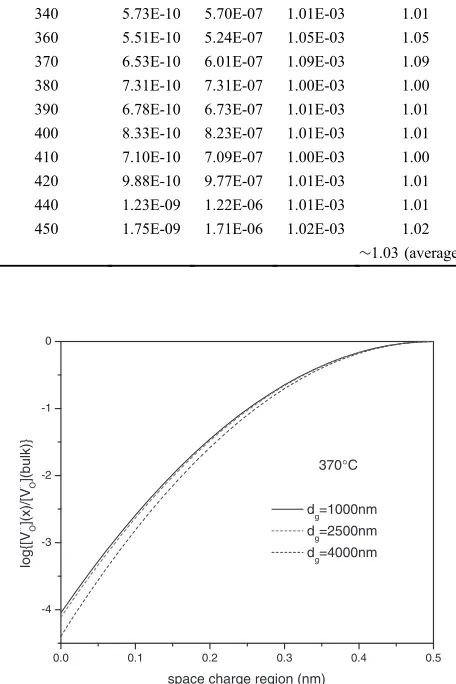
[image:7.595.321.533.69.238.2]ð14Þ Where ½VO••ðxÞ is the oxygen vacancy concentration and s is the thickness of the space charge layer which can be estimated as one half of the grain boundary thickness,¤gb.31) ¤gb could be calculated from the capacitances according to eq. (7). Table 4 shows the fitting result of capacitances at different temperature of 8ScSZ (grain size is 1000 nm) sintered for 2 h. The grain boundary thickness of 8ScSZ samples with the grain size of 2500 and 4000 nm was calculated by the same way. The average value of grain boundary thickness ¤gb is about 1.03, 1.01 and 0.99 nm for the 8ScSZ sample with the grain size of 1000, 2500 and 4000 nm, respectively. Thus the grain boundary thickness is independent of the grain size of 8ScSZ. The oxygen vacancies concentration profile of 8ScSZ is shown in Fig. 13: the oxygen vacancies concentration in the grain boundary space charge region increases with decrease of the grain size.
Fig. 11 HREM image of triple grain junction of 8ScSZ with an average grain size 1000 nm.
Table 3 Sc and Si content of triple grain junction, grain boundary and grain interior, respectively.
Element
mass%
Site 1: triple grain junction
Site 2: grain boundary
Site 3: grain interior
Si 0.1 0.1 0.1
Sc 8.3 8.4 8.3
1.38 1.40 1.42 1.44 1.46 1.48 1.50 1.52 1.54 1.56 1.58 1.60
0.26 0.28 0.30 0.32 0.34
1000nm 2500nm 4000nm
Δϕ(0)
(V)
[image:7.595.49.290.71.255.2]1000/T(1/K)
[image:7.595.46.293.338.406.2]4. Conclusions
(1) Different dopant contents of Sc2O3in ScSZ results in the formation of different crystal structure. 5 and 8 mol% Sc2O3 doped ZrO2 are cubic phase. 10 mol% Sc2O3 doped ZrO2 is mixed by rhombohedral phase and cubic phase. The rhombohedral phase appeared in ScSZ decreases the conductivity of ScSZ, but it can be transformed to cubic phase again when the temperature is above 550°C.
(2) The increase of the dopant content of Sc2O3 leads to the decrease in grain size of ScSZ. But excessive dopant content brings about the re-emergence of the large grain size specifically in 10ScSZ which is attributable to the rhombo-hedral phase decomposed from cubic phase.
(3) The grain boundaries of high-purity 8ScSZ are free of any amorphous phase and without any segregation; the total grain boundary conductivity decreases but the specific grain boundary conductivity increases with the decrease in grain
size of 8ScSZ. As a result, the grain boundary space charge potential decreases and the concentration of oxygen vacan-cies in the space charge regions increase with decreasing grain size.
Acknowledgments
The authors thank Chih-kai Yang (California Institute of Technology) for his assistance with X-ray diffraction microscopy.
REFERENCES
1) R. Chiba, T. Ishii and F. Yoshimura:Solid State Ionics91(1996) 249.
2) W. Huang, P. Shuk, M. Greenblatt, M. Croft, F. Chen and M. Liu:
J. Electrochem. Soc.147(2000) 4196.
3) J. Drennan and G. Auchterlonie:Solid State Ionics134(2000) 75.
4) A. J. McEvoy:Solid State Ionics132(2000) 159.
5) N. Q. Minh and T. Takahashi:Science and Technology of Ceramic Fuel Cells, (Elsevier, Amsterdam, 1995).
6) S. P. S. Badwal:J. Mater. Sci.22(1987) 4125.
7) F. M. Spiridonov, L. N. Popova and R. Ya. Popil’skii:J. Solid State Chem.2(1970) 430.
8) J. D. McCullough and K. N. Trueblood:Acta Cryst.12(1959) 507 511.
9) D. K. Smith and H. W. Newkirk:Acta Cryst.18(1965) 983.
10) C. J. Howard, R. J. Hill and B. E. Reichert:Acta Cryst. B44(1988) 116.
11) G. Teufer:Acta Cryst.15(1962) 1187.
12) P. Aldebert and J. P. Traverse:J. Am. Ceram. Soc.68(1985) 34.
13) R. J. Ackermann, S. P. Garg and E. G. Rauh:J. Am. Ceram. Soc.60
(1977) 341.
14) Y. Oishi and K. Ando:Transport in Nonstoichiometric Compounds, (Plenum Press, 1985) pp. 189202.
15) E. S. Raj, A. Atkinson and J. A. Kilner:Solid State Ionics180(2009) 952955.
16) S. P. S. Badwal, F. T. Ciacchi, M. V. Swain and V. Zelizko:J. Am. Ceram. Soc.73(1990) 2505.
17) S. P. S. Badwal and A. E. Hughes:J. Eur. Ceram. Soc.10(1992) 115.
18) S. P. S. Badwal and S. Rajendran: Solid State Ionics83(1994) 7071. 19) S. P. S. Badwal: Solid State Ionics67(1995) 76.
20) M. Gödickemeier, B. Michel, A. Orliukas, P. Bohac, K. Sasaki, L. Gauckler, H. Heinrich, P. Schwander, G. Kostorz, H. Hofmann and O. Frei:J. Mater. Res.9(1994) 1228.
21) M. Aoki, Y.-M. Chiang, I. Kosacki, J. R. Lee, H. L. Tuller and Y.-P. Liu:J. Am. Ceram. Soc.79(1996) 1169.
22) Y. Arachi, H. Sakai, O. Yamamoto, Y. Takeda and N. Imanishai:Solid State Ionics121(1999) 133.
23) J. Maier:Ber. Bunsenges. Phys. Chem.90(1986) 26.
24) M. J. Verkerk, B. J. Middelhuis and A. J. Burggraaf:Solid State Ionics
6(1982) 159.
25) X. Guo and J. Maier: J. Electrochem. Soc. E211(2001) 148. 26) Y. M. Chiang, D. P. Birnie and W. D. Kingery:Physical Ceramics:
Principles of Ceramic Science and Engineering, (John Wiley and Sons, New York, 1997) pp. 208211.
27) D. S. Lee, W. S. Kim, S. H. Choi and J. H. Lee:Solid State Ionics176
(2005) 3339.
28) F. M. Spiridonov, L. N. Popova and R. Y. Popil’skii: J. Solid State Chem.2(1970) 430.
29) C. Peters, A. Weber and E. Ivers-Tiffee:J. Am. Ceram. Soc.92(2009) 20172024.
30) S. M. Haile, D. L. West and J. Campbell:J. Mater. Res.13(1998) 15761595.
[image:8.595.48.289.105.249.2]31) X. Guo and Z. Zhang:Acta Mater.51(2003) 25392547.
Table 4 Capacitances for bulk and grain boundary at different temperature and thickness of grain boundary of 8ScSZ sintered at 1350°C for 2 h; of which the grain size is 1000 nm.
Temperature (°C) Cbulk(F) Cgb(F) Cb/Cgb ¤gb(nm)
340 5.73E-10 5.70E-07 1.01E-03 1.01
360 5.51E-10 5.24E-07 1.05E-03 1.05
370 6.53E-10 6.01E-07 1.09E-03 1.09
380 7.31E-10 7.31E-07 1.00E-03 1.00
390 6.78E-10 6.73E-07 1.01E-03 1.01
400 8.33E-10 8.23E-07 1.01E-03 1.01
410 7.10E-10 7.09E-07 1.00E-03 1.00
420 9.88E-10 9.77E-07 1.01E-03 1.01
440 1.23E-09 1.22E-06 1.01E-03 1.01
450 1.75E-09 1.71E-06 1.02E-03 1.02
³1.03 (average)
0.0 0.1 0.2 0.3 0.4 0.5
-4 -3 -2 -1 0
log{[V
⋅⋅](x)/[VO
⋅⋅](bulk)}O
space charge region (nm) dg=1000nm dg=2500nm dg=4000nm
[image:8.595.55.283.120.462.2]370°C