Fabrication of the Crystal-Oriented Thermoelectric Material Bi
2Te
3by Slip Casting under a High Magnetic Field
Toshiyuki Kuribayashi
1;*, Mun-Gyu Sung
1, Takashi Itoh
2, Kensuke Sassa
3and Shigeo Asai
11
Dept. of Materials, Physics and Energy Engineering, Graduate School of Engineering, Nagoya University, Nagoya 464-8603, Japan
2Division of Integrated Research Projects, EcoTopia Science Institute, Nagoya University, Nagoya 464-8603, Japan 3Materials Research Institute for Sustainable Development, National Institute of Advanced Industrial Science
and Technology, Nagoya 463-8560, Japan
It is well known that the electric and thermal conductivities of materials depend largely on their crystal orientation. Meanwhile, the imposition of a high magnetic field is a very effective method of obtaining highly crystal-aligned structures. Recently, thermoelectric materials, that is, materials which can directly convert electrical energy to thermal energy and vice versa, have attracted significant attention for their potential uses in solving environmental problems.
In this study, highly crystal-aligned structures of Bi2Te3compact were prepared by introducing crystal alignment into a green sample by conducting slip casting under a high magnetic field, followed by compaction by pulse-discharge sintering (PDS). By aligning the crystal orientation, electric resistivity was reduced, while the Seebeck coefficient maintained a value nearly identical to that of non-aligned crystals. The reference value of a dimensionless figure of merit as high as 1.3 at 323 K was obtained. [doi:10.2320/matertrans.47.2387]
(Received May 15, 2006; Accepted July 20, 2006; Published September 15, 2006)
Keywords: thermoelectric materials, slip casting, high magnetic field, bismuth telluride, electromagnetic processing of materials
1. Introduction
When different temperatures are imposed on two different planes of a thermoelectric material, an electric voltage known thermo-electromotive force is induced between the two planes. This phenomenon is called the Seebeck effect, and the reverse phenomenon, in which a temperature difference between two planes appears when a voltage is imposed on both planes, is called the Peltier effect. By using thermo-electric materials, thermo-electric energy can be generated and substances can be cooled without emitting greenhouse gases. To increase the utilization of thermoelectric materials, a higher conversion efficiency of thermoelectric energy, which is indicated by a higher figure of merit Zð¼2=Þ, is required. That is, a higher Seebeck coefficient, , lower electric resistivity,, and lower thermal conductivity,, are the desirable physical properties to effectively convert thermal energy to electric energy and vice versa.1)
Bi2Te3 is a thermoelectric material known to have crystal anisotropy such that the efficiency of the thermoelectric conversion of Bi2Te3 depends largely on its crystal orienta-tion.2) In this regard, a single crystal of Bi
2Te3 is most desirable, even though it has the disadvantage of low mechanical strength. On the other hand, although pulse-discharge sintering (PDS) can improve mechanical strength and provide fine-grained crystals which lead to lower thermal conductivity due to grain boundary scattering,3) it cannot
fabricate the highly aligned polycrystals which are necessary to reduce the electric resistivity of Bi2Te3.
Recently, it has been recognized that a high magnetic field can be used effectively to control the texture of materials.4) Additionally slip casting is well known to be a useful method of fabricating ceramic compacts with fine-grained crystals.5) In the present study, the thermoelectric material Bi2Te3 was
fabricated with highly aligned fine crystals by performing slip casting under the imposition of a high magnetic field, followed by PDS. The maximum obtained value of the figure of merit was as high as 1.3 at 323 K in the present Bi2Te3 compact.
2. Experimental Methods
When crystals with magnetic anisotropy are submerged in a high magnetic field, they rotate to reduce magnetization energy, which depends on the magnetic susceptibility of each crystal orientation. The magnetization energy of materials submerged in a magnetic field is given by eq. (1).
U¼ B
2
20ð1þNÞ2
; ð1Þ
where B is the imposed magnetic field, the magnetic susceptibility, and 0 the permeability in a vacuum. The magnetic susceptibilities of Bi2Te3in the a,b-axis and the c-axis area;b¼ 3:1106andc¼ 5:5106, respec-tively.6) By substituting the values in eq. (1), the relation
Uc>Ua;bis obtained. This means that single crystals rotate so that the c-axis of the crystals will be perpendicular to the direction of an imposed magnetic field, and it is essential that each particle is made of a single crystal. The present experimental apparatus is shown schematically in Fig. 1. In order to obtain a slurry with fine-grained Bi2Te3 of single crystals, polycrystalline Bi2Te3 powders were milled for approximately 60 min in distilled water with the addition of a dispersant of sodium hexametaphosphate ((NaPO3)6). A vessel containing the slurry was rotated during the slip casting under a horizontal magnetic field of 10T to obtain green samples with uni-directionally aligned crystals.7)The crystal orientation was examined over a span of2from 10 to 60 on the top surface of the green samples by X-ray diffraction (XRD). The micro-structures on the top surface
*Graduate Student, Nagoya University
and cross-section of the green samples were also examined by scanning electron microscopy (SEM).
Green samples with uni-directionally aligned crystals and those with polycrystalline Bi2Te3 powders were compacted by PDS, and the crystal orientation of the compacts was also examined by XRD and SEM.
In order to measure the Seebeck coefficient and electric resistivity of a sample, it must have a thickness of more than 2 mm, which is thicker than the green samples obtained by slip casting in the present study. To eliminate this problem, the crystal-oriented green samples were piled on a zone composed of polycrystalline Bi2Te3 powders before meas-urement, and the resultant test piece was placed into a carbon die for sintering by PDS. For comparison, a test piece composed only of polycrystalline Bi2Te3 powders was also prepared and sintered by PDS. The conditions of the temperature and pressure applied for PDS treatment are given in Fig. 2. From the obtained test pieces, whose diameter was 20 mm and whose thickness was 3 mm, a pillar-shaped specimen of3313mm3was cut for XRD analysis and SEM observation. Electric resistivity was measured under an electric current imposed perpendicular to the pressing direction in PDS, using a four-probe DC method. The Seebeck coefficient was observed under temper-atures differences of 20, 30 and 40 K, which were imposed on the two edges of the pillar-shaped specimen, where the heat flow was perpendicular to the pressing direction in PDS. The
three values obtained under the three temperature conditions were averaged and assigned as the Seebeck coefficient.
Thermal conductivity, , is described by the following equation:8)
¼carþph; ð2Þ
wherecarandphexpress the carrier and lattice contributions
to thermal conductivity, respectively. The value of ph
decreases with decreasing crystal size due to phonon scattering at the grain boundaries.9) Thus, fine-grained
crystals lead to a decrease in thermal conductivity,. Thermal conductivity, was measured by the laser flash method. Since the thin compact composed of the crystal-aligned layer was too thin to be measured by the standard equipment used in this method, a compact composed of crystals which were made by the same procedure as that for the thin compact, except slip casting, was prepared to measure the thermal conductivity. A compact composed of polycrystalline powder was also measured to determine the effect of crystal size.
3. Results
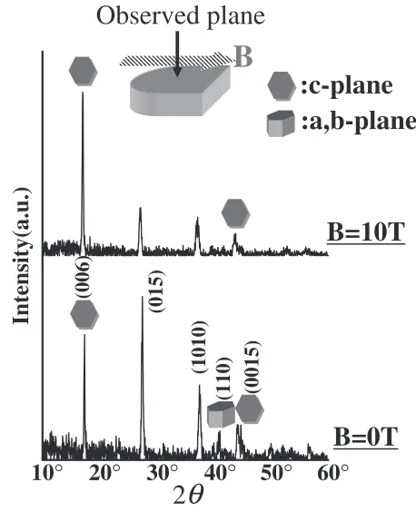
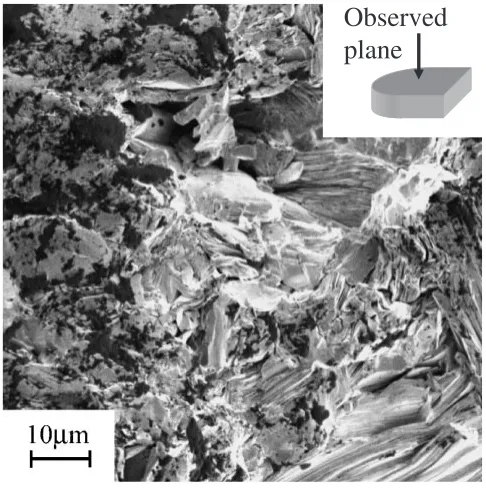
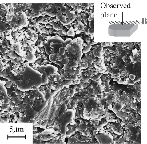
The XRD patterns of the green samples obtained under slip casting with and without the magnetic field are shown in Fig. 3. As can be seen from the two XRD patterns, the relative intensities of the (006) and (0015) planes corre-sponding to the a or b plane to that of the (015) plane increased in the sample obtained by slip-casting under a magnetic field of 10T. SEM pictures of the top surface and cross section of the crystal-aligned green sample are shown in Figs. 4 and 5, respectively. The results of XRD and SEM
B
g
Filter dehydration
Bi2Te3particles
Green sample
g
Super conducting magnet
magnetic field
Vessel for slip casting
Direction of
B
Fig. 1 Experimental apparatus for slip casting under a high magnetic field.
5 10
2K/min
20 min 15 min
473K
773K
3MPa
40MPa 293K
Pressure shift
Temperature shift
min min
Fig. 2 Temperature and pressure conditions of PDS.
10
°
20
°
30
°
40
°
50
°
60
°
Intensity(a.u.)
(006)
(015)
(1010)
(110)
(0015)
B=0T
:c-plane
:a,b-plane
B=10T
Observed plane
B
2
θ
[image:2.595.310.539.74.356.2] [image:2.595.51.290.74.239.2] [image:2.595.55.286.287.426.2]pictures indicate that the crystals were highly aligned by slip-casting under the magnetic field, demonstrating that the imposed magnetic field contributes greatly to crystal align-ment in the green sample.
The XRD patterns of the green sample with aligned crystals and of its corresponding sample by PDS are shown in Fig. 6. The relative intensities of the (006) plane to that of the (015) plane in the sintered and green samples were almost identical, indicating that the degree of crystal alignment in the c-plane was not changed by PDS. The SEM pictures of the top surface and cross-section of the specimens with
randomly aligned crystals and aligned crystals are shown in Figs. 7–10. Based on the present results, it can be concluded that the method of processing developed in this study is useful for fabricating specimens with uni-direction-ally aligned crystals.
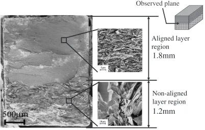
The SEM picture of a cross-section of the sample composed of the crystal-aligned green layer and polycrystal-line powder is shown in Fig. 11, in which the crystal-aligned
Observed
plane
B
Fig. 4 SEM observation of the top of the green sample with aligned crystals.
Observed
plane
B
Fig. 5 SEM observation on the cross-section of the green sample with aligned crystals.
10
°
20
°
30
°
40
°
50
°
60
°
Intensity(a.u.)
Green
sample
Sintered
sample
:c-plane
(006)
(015)
(1010)
(0015)
B
2
θ
Observed plane
Fig. 6 XRD patterns of green sample and its sintered one.
Observed
plane
[image:3.595.49.287.70.303.2] [image:3.595.313.541.75.348.2] [image:3.595.49.290.355.601.2] [image:3.595.305.548.393.637.2]and non-aligned zones are clearly distinguished. In order to calculate a power factor,P(¼2=) and a figure of merit,Z (¼2=), the Seebeck coefficient, the electric resistivity and the thermal conductivity must be evaluated. The temper-ature dependence of the Seebeck coefficient of the specimens with and without aligned crystals is shown in Fig. 12. Throughout the temperature range from 323 to 673 K, the specimens show n-type semi-conductors, indicated by the negative values of the Seebeck coefficient, which do not depend on crystal alignment. This is a reasonable result, since the Seebeck coefficient of a single crystal scarcely depends on crystal orientation.2)
The electric resistivity,, of the composite zones can be expressed as eq. (3) on the basis of a parallel electric circuit rule:
S
L¼
Sa
aL
þ Sn
nL
; ð3Þ
whereSa,SnandSare the cross-sectional areas of the crystal-aligned zone, the non-crystal-aligned zone and the total zone, respectively, a, n and are the electric resistivity of the respective zones and L is the length of the samples. The electric resistivity of the crystal-aligned zone, a, was calculated by substitutingn and obtained in the experi-ment and the measured values ofSa,SnandSinto eq. (3).
The temperature dependence of the electric resistivity is shown in Fig. 13. The electric resistivity of Bi2Te3 was reduced by aligning crystals in the a,b-axis orientation. This agrees with the result2)that the ratioc=a;bof a single crystal is 3.48, that is, the electric resistivity of Bi2Te3is lower in the a,b-axis than that in the c-axis.
The power factor,P(¼2=) evaluated by substituting the value of the Seebeck coefficient at 323 K as shown in Fig. 12, and the value of the electric resistivity of the crystal-aligned layer at 323 K as shown in Fig. 13, is 4:60103Wm1 K2, which is nearly identical to the maximum value reported10,11)for a single crystal,4:64103Wm1K2.
The temperature dependence of the thermal conductivity is shown in Fig. 14. The specimen with fine crystals has lower thermal conductivity than polycrystalline powder specimen over the whole range of temperature because of phonon scattering at the grain boundary.
The values of the Seebeck coefficient, the electric resistivity and the thermal conductivity at certain measured temperatures in the present study were substituted into the equation, Z¼2=. The temperature dependence of the dimensionless figure of merit is shown in Fig. 15. The value
plane
B
[image:4.595.50.289.71.315.2]Observed
Fig. 10 SEM observation on the cross-section of the crystal-aligned compact.
Observed
plane
Fig. 8 SEM observation on the cross-section of the sintered compact without aligned crystals.
plane
B
Observed
[image:4.595.305.548.72.316.2] [image:4.595.49.288.369.604.2]of the aligned layer is larger than that of the non-aligned layer over the entire measured temperature range and the max-imum reference value of the dimensionless figure of merit
is 1.3 at 323 K, which to the best of our knowledge is the highest value reported to date for polycrystalline Bi2Te3. In addition, it must be noticed that this value is used as a 0
2 4 6 8 10 12 14
300 350 400 450 500 550 600 650 700
Electrical resistivity,
/
ρ
×
10
-6
Ω
·m
Composite of crystal-aligned layer and polycrystalline powder Polycrystalline powder Crystal-aligned layer
[image:5.595.98.500.75.331.2]Temperature, T/K
Fig. 13 Temperature dependence of electrical resistivity,.
0 0.5 1 1.5 2 2.5 3
300 350 400 450 500 550 600 650 700
Thermal conductivity,
/W
·
K
κ
-1 m
-1
Fine-grained powder
Polycrystalline powder
[image:5.595.57.283.368.514.2]Temperature, T/K
Fig. 14 Temperature dependence of thermal conductivity,.
0 1
0.2 0.4 0.6 0.8 1.2 1.4 1.6
300 400 500 600 700
Dimensionless figure of merit,
ZT
/- Composite of crystal-aligned layer and polycrystalline powder
Polycrystalline powder Crystal-aligned layer
1.33
Temperature, T/K
Fig. 15 Temperature dependence of dimensionless figure of merit,ZT.
-160
-140
-120
-100
-80
-60
-40
-20
0
300 350 400 450 500 550 600 650 700
Seebeck coefficient,
α
/
µ
V
·
K
-1
Composite of crystal-aligned layer and polycrystalline powder
Polycrystalline powder
Temperature, T/K
Fig. 12 Temperature dependence of the Seebeck coefficient,.
Aligned layer
region
Non-aligned
layer region
1.8mm
1.2mm
[image:5.595.314.543.369.518.2]Observed plane
[image:5.595.314.541.559.709.2] [image:5.595.58.282.560.710.2]reference value, because the value of the thermal conductiv-ity obtained in non-oriented sample was adopted.
4. Conclusions
To fabricate Bi2Te3materials with highly aligned crystals, we introduced a method of slip casting under a high magnetic field and pulse-discharge sintering (PDS). The following results were obtained:
(1) green samples with highly aligned crystals are obtained by performing a slip casting under a high magnetic field;
(2) the degree of crystal alignment in samples sintered by PDS is maintained at the same degree as that in green samples with aligned crystals;
(3) a Bi2Te3 compact with aligned crystals was found to provide the lower electric resistivity and a larger power factor; and
(4) the maximum reference value of the dimensionless figure of merit obtained in the present study is as high as 1.3 at 323 K.
Acknowledgements
This research was supported by the Tatematsu Foundation, the 21st Century COE Program ‘‘The Creation of Nature-Guided Materials Processing’’ and Grant-in-Aid for
Scien-tific Research on Priority Areas (S), number 13852013 from Ministry of Education, Culture, Sports, Science and Tech-nology of Japan. The authors would like to thank Professor M. Mabuchi of the Graduate School of Energy Science and Technology of Kyoto University and Dr. Y. Chino of the Materials Research Institute for Sustainable Development of the National Institute of Advanced Industrial Science and Technology.
REFERENCES
1) S. Sugihara, S. Kawashima, H. Suzuki and R. Sekine: J. Japan Inst. Metals63(1999) 1369–1371.
2) H. Kaibe, M. Sakata, T. Ohkosi, Y. Isoda and I. Nishida: J. Mater. Sci. Soc. Jpn.27(1990) 107–115.
3) N. Miyasita, R. Tsukuda and I. Yashima: J. Japan Inst. Metals 68 (2004) 482–489.
4) S. Li, K. Sassa, K. Iwai and S. Asai: Mater. Trans.45(2004) 3124– 3129.
5) E. P. Hyatt: Am. Ceram. Soc. Bull.65(1986) 637–638.
6) O. Madelung, M. Schulz and H. Weiss: LANDOLT-Bornstein; Zahlenwerte und Funktionen aus Naturwissenschaften und Technik, III-17-f, Springer, 1983, Tokyo, p. 546.
7) S. Li, K. Sassa and S. Asai: Mater. Lett.59(2005) 153–157. 8) I. J. Ohsugi, T. Kojima and I. A. Nishida: J. Appl. Phys.63(1988)
5179.