LEABHARLANN CHOLAISTE NA TRIONOIDE, BAILE ATHA CLIATH TRINITY COLLEGE LIBRARY DUBLIN
OUscoil Atha Cliath The University of Dublin
Terms and Conditions of Use of Digitised Theses from Trinity College Library Dublin Copyright statement
All material supplied by Trinity College Library is protected by copyright (under the Copyright and Related Rights Act, 2000 as amended) and other relevant Intellectual Property Rights. By accessing and using a Digitised Thesis from Trinity College Library you acknowledge that all Intellectual Property Rights in any Works supplied are the sole and exclusive property of the copyright and/or other I PR holder. Specific copyright holders may not be explicitly identified. Use of materials from other sources within a thesis should not be construed as a claim over them.
A non-exclusive, non-transferable licence is hereby granted to those using or reproducing, in whole or in part, the material for valid purposes, providing the copyright owners are acknowledged using the normal conventions. Where specific permission to use material is required, this is identified and such permission must be sought from the copyright holder or agency cited.
Liability statement
By using a Digitised Thesis, I accept that Trinity College Dublin bears no legal responsibility for the accuracy, legality or comprehensiveness of materials contained within the thesis, and that Trinity College Dublin accepts no liability for indirect, consequential, or incidental, damages or losses arising from use of the thesis for whatever reason. Information located in a thesis may be subject to specific use constraints, details of which may not be explicitly described. It is the responsibility of potential and actual users to be aware of such constraints and to abide by them. By making use of material from a digitised thesis, you accept these copyright and disclaimer provisions. Where it is brought to the attention of Trinity College Library that there may be a breach of copyright or other restraint, it is the policy to withdraw or take down access to a thesis while the issue is being resolved.
Access Agreement
By using a Digitised Thesis from Trinity College Library you are bound by the following Terms & Conditions. Please read them carefully.
Scanning Near-Field Microscopy
of Microwave Circuits
A thesis submitted to the University of Dublin, Trinity College, in
application for the degree of Doctor in Philosophy
4 .
Rom an Kantor
Physics Department
Trinity College Dublin
TRWITY C O L L E G E ^ 1 0 0 c jjti0 2 _
ii
Declaration
This thesis is subm itted by the undersigned for the degree of Doctor in Phi
losophy at the University of Dublin. It has not been submitted as an exercise
for a degree at any other university.
A part from the advice, assistance and joint effort mentioned in the ac
knowledgments and in the text, this thesis is entirely my own work.
I agree th at the library may lend or copy this thesis freely on request.
Acknowledgments
First, I would like to thank Prof. Igor Shvets for inviting me to join his
excellent group and to work on an interesting project. I have enjoyed a lot of
independence during past years but he was always here ready to help when
something went worse. I am thankful for his support during those years.
Shane gave me a shelter after my arrival to Dublin and he still shares a
house with me. He probably regrets th at by now... I hope Dima, Sergei and
Victor enjoyed our lunch discussions and philosophical arguments as much
as I did (although it is difficult to have argument with Sergei!). I want to
thank Anselm for his fabulous cakes, Vivienne for being so nice, William
for his probes, Diadmaid for enjoying the spa wafers, Ciaran and Jurgen for
their good mood, Luca for being Luca. And I “thank” Guido for permanently
beating me in squash. A bunch of new guys - Sergio, Alex, Ken and Giuseppe
- joined the group recently, I hope there will be soon an occasions to go for
a pint...
My thanks go also to Michal, Nikolai and Michael for their help and
contribution to the project. I am also very grateful to all the departm ental
staff: Tom, Marie, Michele, Susan, Elaine, John, Mick, James, Dave and
others, without their everyday help we would be completely lost. I would
like also to acknowledge my colleagues from my past work, especially Prof
Pistora who supported my departure here.
A bstract
The topic of this thesis is the development and testing of measurement tech
niques for high resolution imaging of the field induced by microwave circuits
in the near-field region. The theoretical aspects of the near-field acquisition
are given and all alternative approaches to the practical realization of the
measurement set-up are studied. The measurement system not only incorpo
rates various instrum entation techniques used in Scanning Probe Microscopy
(SPM) and microwave electronics but also incorporates new alternative tech
niques developed to solve the specific problems of the experiment.
The author has focused his attention on acquisition of electric field in
tensities induced by microwave devices. Using a microwave Vector Network
Analyzer (VNA) both the amplitude and the phase of a microwave field
are acquired by m iniature coaxial antennas. High resolution probes were
equipped with a low-noise preamplifier for efficient signal matching to the
following microwave network. A new position-diff^erence method for spatial
resolution enhancement is theoretically analyzed and numerically verified us
ing the Moment Method (MM). The effect of the resolution increase (down
to about 10/xm) is demonstrated on various samples and it is found th a t res
olution achieved allows for inspection of most hybrid and many integrated
circuits. Special antenna configurations are used for acquisition of all spatial
components of the electric field vector. The probes are calibrated in a well-
defined field standard to render quantitative description of the field intensities
possible.
utilizes the Quartz tuning fork, commonly used in Scanning Near-Field Op
tical Microscopy for tip/sam ple separation control and which operates in the
mode where a tip oscillates parallel or perpendicular to the sample surface.
The topography probe allows relatively fast scanning (up to several hun
dreds /xm/s) over rough surfaces with step-like structures. The measurement
process is controlled by an in-house developed software which also allows the
visualization and basic post-processing of the acquired data.
List of Figures
1.1 Measurement of the field intensities by small a n te n n a s...
17
2.1 Radiation from a current e l e m e n t...
22
2.2 Configurations of transmission l i n e s ...
28
2.3 Field discribution above a coupled line in vertical configuration 31
2.4 Field distribution above a coupled line in the horizontal con
figuration ... 32
2.5 Field of surface ch arg es... 34
2.6 Microstrip transmission line configuration... 37
2.7 Field of a microstrip transmission lin e ... 39
2.8 Contribution of the surface charge to the normal electric field
intensity
... 41
3.1 Separate scanning of the sample topography and the field. . .
48
3.2 Standard configuration of SF tuning fork system... 50
3.3 Resonation of the tuning fork arms in standard configuration .
53
3.4 Single oscillating arm c o n fig u ra tio n ...
55
3.5 Resonance curve of the single oscillating arm configuration . .
56
3.6 Comparison of the tip appoach curves for standard and single
oscillating arm c o n fig u ra tio n s ... 57
3.7 Long-probe SF configuration... 58
L IS T OF FIGURES
vii
3.8 Shear-force interaction for a blunt tip
...
59
3.9 Influence of a surface water layer on the tip oscillation . . . .
60
3.10 Touching mode of the coupling of oscillations between the
probe and the f o r k ... 62
3.11 Resonance and approach curves for touching more of oscillation
c o u p lin g ...
63
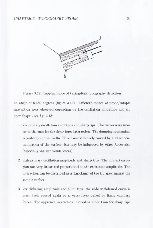
3.12 Tapping mode of tuning-fork topography detection ...
64
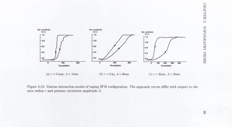
3.13 Various interaction modes of taping SFM configuration . . . .
66
3.14 Schematics of the fork p l u g - i n ...
70
3.15 Influence of the probe geometry and placement on the scanning
s p e e d ...
74
3.16 Topography tips and the antenna wire...
75
4.1 Short monopole antenna...
77
4.2 Electrical equivalent schematics of a short m onopole...
78
4.3 Electric antenna c ro ss -s e c tio n ...
80
4.4 Electric field antennas ... 82
4.5 The design of the a n t e n n a ... 85
4.6 Antenna re sp o n se ... 86
4.7 Calibration u n i t s ... 87
4.8 Position-difference method... 89
4.9 Calculated and measured antenna signals above a cylindrical
transmission line... 95
4.10 Dependency of the signal on antenna displacem ent... 97
4.11 Probe configuration for measurement of all spatial components
of the fie ld ... 99
L IST OF FIGURES
viii
5.2
Michelson interferometer and photo-detection circuit
...104
5.3
Scanning control system sc h e m a tic s... 107
5.4
Principle of the feedback f u n c tio n ... 109
5.5
Schematics of the feedback amplifier ...110
6.1
Topography scan of an EPROM m e m o ry ... 114
6.2
Topography of a Lange coupler ... 115
6.3
Fast topography scanning of a silicon wafer with step struc
tures
116
6.4
Topography of a distrubuted PCB f ilte r...118
7.1
Electric field of a microstrip transmission l i n e ...122
7.2
Distribution of the signals across the m ic r o s tr ip ...123
7.3
Comparison of the measured field with calculated electric in
tensity
124
7.4
Topography of the c a p a c ito r ...125
7.5
511 scattering coefficient of the structure with a PCB capacitor 126
7.6
Effect of resolution enhancement for surface c a p a c ito r...128
7.7
Signal intensities across the fingers of the c a p a c i t o r ... 130
7.8
Signal intensities across the signal feeding line of the capacitor 131
7.9
Fields of the capacitor for non-resonant excitation frequency . 132
7.10 Measurement of tangential field c o m p o n e n ts ... 133
7.11 Field of a microstrip f i l t e r ... 135
7.12 Microstrip m e a n d e r... 136
A .l Various a n t e n n a s ... 141
A.2 Bias coupler d e s ig n ... 142
A.3 DC bias c o u p le r...143
L IS T OF FIGURES
ix
List of Tables
2.1 Field components of an infinitesimal d ip o le ...
23
2.2 Calculation of the fields of a coupled transmission lin e ...
29
2.3 Response functions of surface c h a r g e s ...
35
4.1 Antenna c o m p o n e n ts...
80
Contents
1
Introd u ction
14
1.1 Objectives of the w o r k ...
14
1.2 State-of-the-art of microwave near-field m e a s u re m e n ts ...
15
2 P rin cip les o f near-field m easu rem en ts
19
2.1 Field of elem entary s o u rc e s ...
20
2.1.1 Fields of a short d i p o l e ...
22
2.1.2 Electric intensity of oscillating c h a r g e s ...
25
2.2
Models of circuit field s o u r c e s ...
27
2.2.1 Two-wire transm ission line of infinitesimal cross-section
27
2.2.2 Electric fields of surface c h a r g e s ...
30
2.2.3 M icrostrip transm ission l i n e ...
36
2.3 Recovery of the circuit s i g n a l s ...
40
2.3.1 Single-layered planar c irc u its ...
40
2.3.2 Multi-layered c i r c u i t s ...
44
3 Topography probe
46
3.1 Shear-Force (SF) d e t e c t o r ...
49
3.1.1 Tuning fork SF o s c illa to r...
50
3.1.2 Single oscillating arm d e s ig n ...
54
C O NT EN T S
xii
3.1.3 Touching geometry of oscillation coupling between the
fork and the p r o b e ...
60
3.2
Tapping mode scanning force distance c o n t r o l ... 63
3.3
Measurement of oscillation a m p litu d e ...
67
3.4
Self-excitation regime of the tuning fork ...
68
3.5
Velocities of the probe m o t i o n ...
71
3.5.1 Stability of the feedback s y s te m ...
71
3.5.2 Scanning v e lo c ity ...
73
3.6
Topography t i p s ...
74
4 E lectric field probes
76
4.1
Short monopole a n te n n a s... 76
4.1.1 Realization of the antennas ...
79
4.2
Sensitivity of the p r o b e s ... 82
4.2.1
Calibration of the antennas ... 84
4.3 Position-Difference (PD) method ... 88
4.3.1 Analysis of the position-difference m e t h o d ... 89
4.3.2 Numerical and experimental verification of the method
94
4.4
Acquisition of tangential components of the fie ld ... 96
5 Scanning set-u p
101
5.1 Probe displacement sy ste m ... 101
5.2 Scanning c o n tro lle r... 105
5.2.1 Feedback a m p lif ie r ...108
5.2.2 Scanning control and data visualization software . . . . 108
5.3
Scanning p r o c e s s ... 112
C O NT EN T S
xiii
7
E lectric field
in ten sity m easu rem en ts
119
7.1
Testing of the position-difference m e th o d ...119
7.1.1
Fields of a strip line ... 119
7.1.2
Fields of a distributed PCB c a p a c ito r... 121
7.2
Acquisition of tangential field c o m p o n e n ts ...129
7.3
Scanning of various s a m p l e s ... 134
8
C onclusion
137
8.1
Achieved re s u lts ... 137
8.2
Further work and improvement of the developed methods . . . 138
A C om ponents o f th e scanning
sy stem
140
Chapter 1
Introduction
1.1
O bjectives of the work
In recent decades the most significant advances in microwave technology were
achieved in the development of solid-state devices and circuits. Rapid devel
opment of communication technologies is accompanied with the mass pro
duction of microwave devices. As miniaturization and low-cost production
capabilities play a key role for their wide incorporation into various devices,
high effort is put into the innovation of microstrip, hybrid and integrated
circuits - the most common elements of communication systems.
The development of new complex microwave circuits is accompanied by a
long and costly process of device testing and modifications. In many cases it
is based only on the designers experience due to the lack of detail information
about the device signals and the distribution of its electromagnetic field. Con
tem porary inspection systems of microwave circuits are usually based on the
measurement of the signals on the device ports. Such measurements, in most
cases only the measurement of the input and output signals, are not sufficient
for characterization of the functionality of particular device subsystems. In
CHA PTE R 1. I NT ROD UC TI ON
15
some cases special measurement pads are designed for direct probe coupling.
Unfortunately their use is limited due to their relatively large contact areas
and their influence on the circuit properties, caused by its relative high capac
itance and cross-coupling with other circuit element. Additionally the load
impedance of the measuring probes can change working regime of the circuits.
These drawbacks effectively eliminate their use in highly miniaturized circuits
- especially in MMIC (Monolithic Microwave Integrated Circuits). Due to the
above mentioned reasons non-contact scanning near-field techniques may be
come an attractive method for circuit performance and failure testing. By
analyzing the field distribution of working circuits one can evaluate not only
signal coupling between circuit parts, the electromagnetic emissions of the
device and other aspects of electromagnetic compatibility (EMC), but also
to describe quantitatively the field sources (charges/potentials, currents) [1, 2]
and the flow of the circuit signals.
1.2
State-of-the-art of microwave near-field m ea
surem ents
C H A P T E R 1. I N T R O D U C T I O N
16
were proposed to optimize their performance [4, 5, 6, 7, 8], for microwave
frequencies conductive transmission lines (such as coaxial structures [9, 10])
are mostly used instead of waveguides with apertures to avoid the cut-off
frequency limitation and for better signal matching to following microwave
network.
The techniques used in scanning near-field microwave microscopy (SNMM)
can be classified according to type of the source signal and the detectors used
for the field acquisition. The microwave field can be generated by an exter
nal source and scattered from the sample in transmission or reflection mode,
i.e. it can be generated by either the probe or the sample itself. As we
will measure the field induced by active (working) microwave circuits, our
considerations will be limited to the last case.
There are several possible approaches on how to detect the field induced
by microwave devices or other samples. They differ by the configuration of
the probes and the type of electro-magnetic interaction between the field
source and the detector:
• use of aperture probes. In many cases modifications such as slit probes
[11, 12] and open-ended transmission lines [13, 14] are used to increase
signal matching efficiency.
• use of a metal tip to which the signal is coupled by electromagnetic
interaction of the concentrated field between the sample and the sharp
tip apex and by capacitance between the probe and the sample. These
techniques have good resolution and much higher sensitivity than aper
ture probes.
CHAPTER 1. INTRODUCTION
17
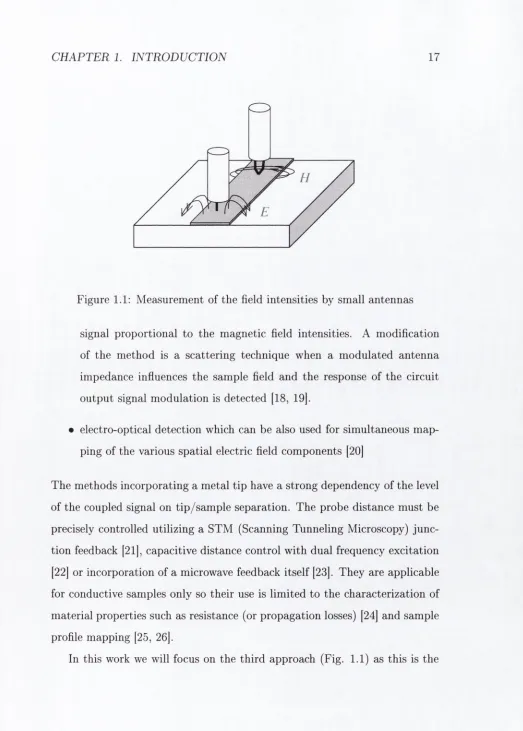
Figure 1.1: Measurement of the field intensities by small antennas
signal proportional to the magnetic field intensities. A modification
of the method is a scattering technique when a modulated antenna
impedance influences the sample field and the response of the circuit
output signal modulation is detected [18, 19|.
• electro-optical detection which can be also used for simultaneous map
ping of the various spatial electric field components [20]
The methods incorporating a metal tip have a strong dependency of the level
of the coupled signal on tip/sam ple separation. The probe distance must be
precisely controlled utilizing a STM (Scanning Tunneling Microscopy) junc
tion feedback [21], capacitive distance control with dual frequency excitation
[22] or incorporation of a microwave feedback itself [23]. They are applicable
for conductive samples only so their use is limited to the characterization of
material properties such as resistance (or propagation losses) [24] and sample
profile mapping [25, 26].
[image:19.542.14.537.39.770.2]Chapter 2
Principles of near-field
measurements
Because of the complexity of the general description of electromagnetic inter
action between the field source and the receiver, in many cases the model of
signal coupling is simplified by splitting the problem into two separate parts:
description of the field induced by the source and the influence of th at field
on the receiving antenna. Such an approximation is appropriate as long as
the m utual coupling between the source and the receiver is low and the in
fluence of the receiving antenna on the transm itter (and its generation of the
primary field) can be neglected. This is mostly the case with our field inten
sity measurements although we have to admit th a t this low coupling, which
avoids the distortion of the circuit signals and the measured field, comes at
the expense of lower levels of the detected signal.
CH APTE R 2. PRINCIPLES OF NEAR-FIELD M E A SU RE M E N TS
20
2.1
Field of elementary sources
The excited electromagnetic field depends on the spatial distribution of the
sources - electric currents and charges. As the field sources vary in tim e the
system quantities can be transformed by Fourier analysis to the frequency
domain and each frequency can be handled separately. This approach also
suits our measurement methods as a single d ata set (for an image of the field
distribution above the circuit) is taken for a particular microwave frequency
and the measured results can be directly compared with quantities calculated
for th a t frequency. The physical quantities can be written in harmonic form
- i.e.
3 { t) =
B
•
exp{iujt) - and the time-dependent factor can be eventually
removed from the formulas. Excluding static fields from our consideration
we can directly link electric charges and current fiow using the continuity
theorem
and both can be interchangeably taken as a source of the excited field. A
convenient method for the field description is the use of scalar and vector
potentials
4>,
A
defined upon the Maxwell equations and vector identities
V • (V
XA) = 0, V
X(V0) = 0
in the form
For complete definition of vector potential
A
its divergence has yet to be
specified. Thanks to this ambiguity a well-suited Lorentz condition can be
introduced
V • j -f
iujp =
0
(2.1)(2.2)
(2.3)
B = V
XA
C H APTER 2. PRINCIPLES OF NEAR-FIELD M EA SU R E M E N T S
21
which allows simplification of the wave equations for scalar and vector po
tentials, in a time-independent form also called the Helmholtz equations
Using the Dirac unit impulse for the infinitesimal source normalization [28]
the solution of these wave equations can be obtained as a collection of con
tributions of all elementary sources, the field potentials become the integrals
over the source volume
where ^
^ = cjy'/ioCo is the propagation constant and r is the distance
away from the source location.
Note th at neither the field sources (charges and current densities) nor
the potentials themselves are independent physical quantities as they have to
fulfill the continuity theorem (2.1) respectively Lorenz condition (2.4). This
allows complete field description using a single vector function A from which
both electric and magnetic intensities can be derived:
Co
V^A +
= -^(oj
(2.5)
j
(2.6)
(2.7)
B
(2.8)H
— V XA
/^oCH AP T E R 2. PRINCIPLES OF NEAR-FIELD ME A S UR E ME NT S
22
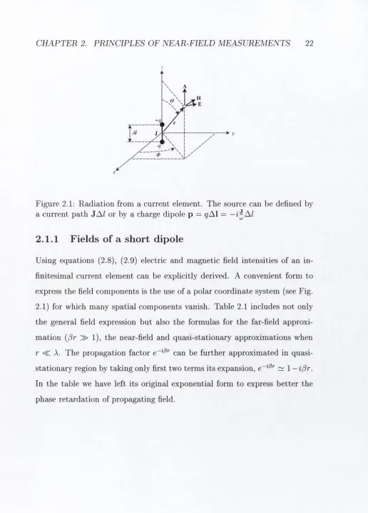
Figure 2.1: Radiation from a current element. The source can be defined by
a current path
J A l
or by a charge dipole p = gAl =
—i ^ A l
2.1.1
F ields o f a short dipole
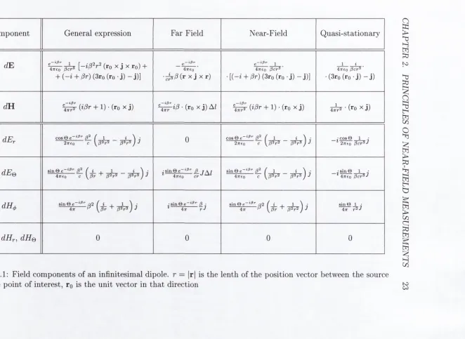
[image:24.542.15.531.36.754.2]C o m p o n en t G en eral expression F ar Field N ear-F ield Q u a si-sta tio n a ry
d E ^ XJ Xro) +
+ ( - i + /3r) (3ro (ro • j) - j)]
47TC0 ■ ^ ^ { r X j X r)
e-iSr 1 47T€o /3cr^
• [ ( - i i + /9r) (3ro(ro -j) - j)]
_L___i . 47TC0 0cr^ ■ (3ro (ro • j) - j)
d U (z/3r + 1) ■ (ro x j) ^ i / 3 - ( r o x j ) A / [ i f i r + 1) ■ (ro X j) 4 ^ • (ro X j)
d E r C08Se~*^*' 0^ ( 127reo c y * ^ -iJ J 0 coB0e“*^'’ ^^ 27reo c ^ /3^r^ ( 1 * ^ 'Ij ^ ,• cos e 27ito 0cr^ J1 ,■
d E s sin0e~*^^ 47reo c i \ 1 ^ ^ i \ 0 r J J
■sinee--®’- 47reo cr
sin0e-*^" 0^ ( 1 i \ ^ 47T€o C y 0 ^ ^ J J
i 8in e 1 ■ 47TC0 0cr^*'
d H ^ sm0e“*^^ 47t ^ o2 ( i t ^ \ jJ J * ■ s m e e - ' » " 0 -47t r-? sin©e~*^^ 47t ^ o2 ( i , 1 t sin 0 1-0^r^ J ^ 4n
dEjfp^ d U f, d H ^ 0 0 0 0
Table 2.1: Field components of an infinitesimal dipole, r =
|r|
is the lenth of the position vector between the source
and the point of interest, tq is the unit vector in th at direction
[image:25.816.143.805.40.523.2]C HAPTER 2. PRINCIPLES OF NEAR-FIELD M EASUREMENTS
24
In many cases an ideal electric dipole is used as a model of an elementary
source. It can be derived from a small (A/
A, ) current path with uniform
amplitude along its length and represented by an infinitesimal wire conductor.
The current causes charge accumulation at the ends resulting in the moment
p =
qAl, the charges can be obtained using the continuity theorem (2.1) for
which
q =
f
The induced vector potential, parallel to the
dipole, can be directly expressed from (2.7) by substituting
f jd^r = JA I =
iup
A =
(2,10)
47rr
The formulas for the field intensities are analogous to the ones in table 2.1
and the quasi-stationary case of electric intensity is identical to the results
obtained by the electrostatic Coulomb’s law for a dipole of two point charges
+q, —q separated by a small distance
Al
The relative phase difference between the electric and magnetic intensities
in the stationary region is 90 degrees and they can be handled separately. The
relation for a stationary magnetic field is usually written as a function of the
current as it resembles the Biot-Savart law,
=
(2-13)
CHAPTER 2. PRINCIPLES OF NEAR-FIELD M EA SU RE ME NT S
25
by the free space impedance
Z = ^ = — =
377Q
H
eoc
(2.14)
The errors of the near-field approximations can be estimated by compar
ison of the terms proportional to
r~^
and
r~^.
Operating at distances
errors can be estimated below 0.25% for the near-field approximation and
below
5%
using the quasi-stationary model of the radiation of the sources.
The real uncertainties caused by these approximations can be expected to be
even smaller as the contribution of closer sources (with smaller errors) to the
total field is larger than the contributions at the sources area boundaries.
2.1.2
Electric intensity of oscillating charges
In near-field region it is more convenient to express the solution for electric
field intensity as a function of the charges - not currents. In accordance with
the formulas in table 2.1 and limiting our consideration to stationary case
each component of the electric intensity can be written in the form
where
xqrepresents the unit vector of the x-coordinate. If we express
of about A/10^ with the area of contributing sources smaller than A/10^, the
(2.15)
using continuity theorem (2.1) and substituting the term
C HAPTER 2. PRINCIPLES OF NEAR-FIELD MEASUREMENTS
26
into (2.15) we get the electric intensity for
x coordinate
The second integral in equation (2.18) can be transformed using Gauss-
Osrtogradski theorem to the surface integral encapsulating the source volume
and it can be set to zero if we assume that all currents are limited to the source
volume. Using similar formulas for other components we get eventually
which resembles well known Coulomb’s law of electrostatic field.
Note that we are allowed to use the stationary model under two impor
tant conditions: the sources are close enough so /Sr
1 and there should be
no external currents to fulfill (2.19). Obviously our microwave circuits are
supplied by the external sources. Fortunately all those signals are coupled to
the inspected region by balanced^ transmission lines where each pair of con
ductors (or the main conductor and the grounding) carries opposite currents
so that this condition is well satisfied.
This approximate formula provides important information about the char
acter of the electric field close to the sources: the electric intensity depends
on the particular result of circuit currents - the charge distribution, to a
much lower degree it depends on the paths of the currents which influence
^The term “balanced line” is used here to express the current symmetry - not the symmetry of the potentials relative to a grounding as often used in radio and microwave engineering
CH APTER 2. PRINCIPLES OF NEAR-FIELD M E A SU RE M E N TS
27
only the far-field components. Because different configurations of the current
lines may lead to a similar spatial distribution of charges, measurements of
the electric intensities in near-field region provides information about those
charges but poorly describes the currents themselves. To some extent the in
formation about them may be retrieved by comparison of the measured d ata
with full-wave electromagnetic field solutions for a particular configuration of
circuit signal lines. In this way, by measuring the distribution of the electric
field along uniform transmission line with known propagation laws, the signal
currents may be also recalculated.
In some situations the static formulas match precisely the full-wave re
sults. This is the case of straight conductors in homogeneous media guiding
harmonic TEM waves such as straight wires, two-wire lines, coaxial trans
mission lines. In the following section we will use the stationary model to
characterize the field of those transmission lines.
2.2
M odels of circuit field sources
2.2.1
Two-wire transm ission line of infinitesim al
cross-section
Due to the high capacitances of the microwave circuit elements and radiation
losses at high frequencies, all the signal transmission is carried by a pair of
coupled lines: either balanced (such as coplanar strips and slot lines) where
symmetric conductors carry electrical currents and potentials, or unbalanced
ones (microstrips, coplanar waveguides) where the main conductor carrying
the signal induces a secondary image of the currents and charges in the near
by grounding.
CHAPTER 2. PRINCIPLES OF NEAR-FIELD M EA S U RE M E NT S
28
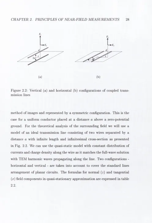
(a) (b)
Figure 2.2: Vertical (a) and horizontal (b) configurations of coupled trans
mission lines
method of images and represented by a symmetric configuration. This is the
case for a uniform conductor placed at a distance
a
above a zero-potential
ground. For the theoretical analysis of the surrounding field we will use a
model of an ideal transmission line consisting of two wires separated by a
distance
a
with infinite length and infinitesimal cross-section as presented
in Fig. 2.2. We can use the quasi-static model with constant distribution of
currents and charge density along the wire as it matches the full-wave solution
with TEM harmonic waves propagating along the line. Two configurations -
horizontal and vertical - are taken into account to cover the standard lines
arrangement of planar circuits. The formulas for normal
(z)
and tangential
(x)
field components in quasi-stationary approximation are expressed in table
[image:30.539.29.526.32.762.2]CH APTER 2. PRINCIPLES OF NEAR-FIELD M EA SU RE M E N TS
29
Finite distance
2a
Infinitesimal separation
2a
E ,
E x
H,
9 ^ 1
z + g
x'^+ {z+ a)'^
( X I
x ^+ {z+ a )'^
X X y
x ^ + ( z + a ) ^ J
Z —a z + d )
2aq
2 7 r e o ( l 2 - f 2 2 ) 211 2 x z
O n T . 1
27T (i2 + ^ 2 ) 2
2 a /
[image:31.541.17.532.28.769.2]CHAPTE R 2. PRINCIPLES OF NEAR-FIELD M EA SU REM ENT S
30
R eso lu tio n lim it
One of the primary goals of the circuit field mapping is localization and quan
titative description of the signals. W ith increasing separation between the
sample, the probe field intensity decay and spatial contrast decrease due to
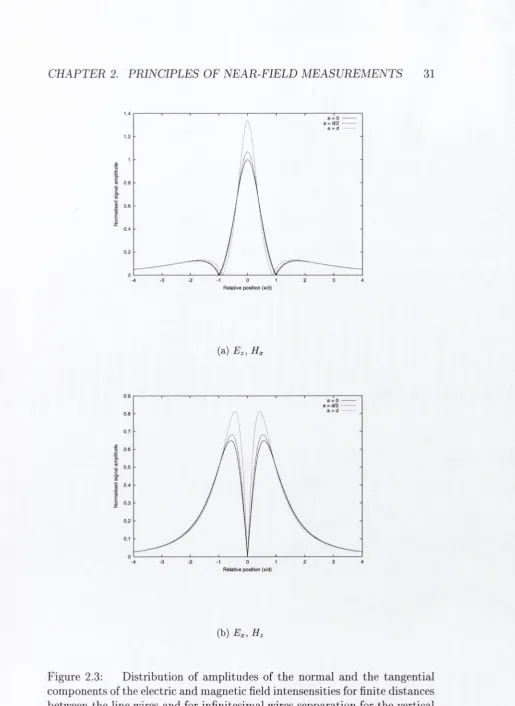
field dispersion. Figure 2.3 represents the field distribution of the electric and
magnetic components above a transmission line in the vertical configuration,
calculated according to the formulas in table 2.2. The dimensions of the field
image scale directly to the probe distance and the width of the field maxi
mum compares directly to the probe separation. This gives us an expected
general rule for the measurement strategy; to achieve images of a certain
resolution, the scan has to be performed at a probe distance comparable to
or smaller than the desired resolution,
z ^ R.
On the other hand the field at
higher distances is more homogeneous with a better defined probe response.
Additionally, if the probe is too close to the sample its presence may cause
redistribution of the circuit sources at immediate distances and distortion of
the measured signals due to its influence on the circuit.
Figure 2.4 shows a two-wire line in the horizontal configuration and can
be used as a model for various coplanar structures such as slot lines and
coplanar waveguides. For a line separation exceeding the distance of the field
probe (a » (i, a =
in the figure) the sources should be considered rather
as separate lines and the infinitesimal dipole approximation is no longer valid.
2.2.2
Electric fields of surface charges
Microwave planar circuits consist of a single or several layers with conductive
signal lines separated by dielectric films. We will describe one of the most
common configurations, a single layered circuit with or without grounding.
C H A P T E R 2. P R IN C IP L E S O F N E A R -F IE L D M E A S U R E M E N T S 31
a = 0 ---= d/2 ... a s d ...
'•5. E CO
1
0.6 o Z 0.4 0,2 1 3•3 -2 -1 0 2 4
-4
Relative position (x/d)
(a) Ez, Hx
0.9 0.7
I
0.5 c o> S5I
0.4 iI 0.3
0.2
0.1
-3 0 1 2 3
-4 -2 •1 4
Relative positkxi (x/d)
(b) E*, H,
[image:33.540.17.533.22.729.2]CHAPTER 2. PRINCIPLES OF NEAR-FIELD MEASUREMENTS
32
0.7 0.5I
Q. E 0.4 (0 c o>1
0.3 (0 § o z 0.2 0.1•10 -5 0 5 10
Relative position (x/d)
(a) E j, H x
1 0.8 0.6 0.4 0.2 0
•10 •5 0 5 10
Retative position (x/d)
[image:34.540.12.529.20.716.2](b)
Ex, H,
CHAPTER 2. PRINCIPLES OF NEAR-FIELD M EA SU REM EN TS
33
written as an integral over the source area
F { x , y , z ) =
J J
g{x
- x ' , y - y' , z) p {x ', y ') d x d y
(2.21)
where
F{x, y, z)
may represent any particular scalar or vector field quantity -
potential
(p
or components of electric intensity E. The function
Q -
which has
yet to be specified - is a corresponding weighting function and represents the
contribution of an infinitesimal source to the total field for defined distance
between the source and point of interest. If the charges would be located in
free space the relation could be directly expressed using equation (2.20). In
our case the charges induce the secondary field sources by polarization of the
dielectric film and by the induction of the surface charges on the conductive
grounding. The influence of these additional sources on the field can be
described by their substitution with virtual charge images screened on the
media boundaries. The position of the images can be obtained by multiple
reflection of the original source at the interfaces as demonstrated in figure
2.5 for a single layered structure with grounding. Knowing the positions and
quantities of the charge images the response functions can be expressed as
a sum of the fields induced by those charges, table 2.3 summarizes the field
CH APTER 2. PRINCIPLES OF NEAR-FIELD M E A SU RE M E N TS
34
(a)
(b)
f A A If
2d
q
-0--
q
q
£^+\
- 4 f .
ie.+lf
- 4 e . ( I
-- -- 0 -- q
{ e^+l f
U + ^rJ
A ( \ A*
-4g,
1-g.
Configuration Charge response function Q
Dielectric surface
D ielectric slab
-•
---Dielectric slab with grounding
2 Cr + 1
2 Cr+1
- x ' , y - y' , z )
. __ / \ 2 n —1 1
T { x x , y ? / ,2) + y : ^ x ; n = i ( ^ ) ^ '> 2 / y ' , z + a[n + l])
\^T{x x , y y , z ) E „ = o ( ! + « ; : ) ' y ' , 2: + 2 a [ n + 1 ] ) ]
Field quantity Field function T
Intensity Ex^ Ey,
Potential (j)
t:EzI ^ rr-Ev _ S / - ( x ^ 2 - ( x 2 + j / 2 + ^ 2 ) - §
' ’ '' 47TC0 ’ 47T£o ’ 47reo
y , x ) ^ ^ {x^ + y^ + z'^y^
CO
Table 2.3: Response function o f surface charge for various structures. The field function T should be substituted w ith the expression presented at the bottom of the table.
CH APTER 2. PRINCIPLES OF NEAR-FIELD M E A SU RE M E N TS
36
In general it is impossible to express explicitly the field summation of an
unbounded series in the presented formulas. In most cases the calculation can
be limited to the first several charge images, the number of iterations depends
on the dielectric permitivity. For high dielectric constant with strong charge
reflections on the boundaries the number must be higher and the field sources
are distributed in a wider area.
2.2.3
M icrostrip transm ission line
One of the most common types of transmission lines used for signal transmis
sion in planar circuits is a microstrip - a uniform conductor separated from
zero-potential grounding by a dielectric material (see Fig. 2.6). Microstrips
are often used in all kinds of planar circuits due to their low production costs,
relatively low transmission losses and low radiation. Possibility of integra
tion with additional microwave elements - both shunt and distributed - and a
relatively wide range of characteristic impedances makes them a good choice
for application in hybrid and monolithic integrated circuits. A comparison of
various guiding media can be found in [30].
Basic parameters characterizing the transmission line - its capacity
C
and inductance
L
per unit length (and its characteristic impedance
Z
=
V L - C - ^ )
can be used to express the signal transmission between the line
ports - input and output. To describe the field distribution, a complete
characterization of the microstrip is required with the width and thickness
of the strip conductor, the permitivity and thickness of the dielectric, the
line termination. Each line has to be solved individually, numerical methods
have to be used (mostly FDTD - Finite Difference Time Domain) to find
a full wave solution for the particular line configuration. Nevertheless for
C HAPTER 2. PRINCIPLES OF NEAR-FIELD MEASUREMENTS
37
Figure 2.6: Microstrip transmission line configuration
and lines with losses |31], a quasi-TEM^ (Transverse Electric and Magnetic)
approximation can be used for two harmonic waves propagating in opposite
directions along the line.
We will limit our consideration to lines with infinitesimal thickness
w ^ t.
To calculate the surrounding electric field we need to find the distribution of
charges
p{x')
across the line and then to calculate the field induced by those
charges. We can use the method of images as presented in table 2.3 to express
the induced field, the only difference is that for uniform distribution of the
charges along the line we will define the source element as a small strip of
infinite length and small width
dx
(see Fig. 2.6) for which the field functions
will be
= ; - ^ l n
27reo
ro
= — , ^ (2 .22 )
27reo
CHAPTER 2. PRINCIPLES OF NEAR-FIELD M EA SU REM EN TS
38
where the zero-potential level ro can be set equal to unity. To find the dis
tribution of the charges across the strip it is necessary to find the solution of
the electrostatic Poisson equation which in our case can be written
II
Q'^{x — x ' , z = 0)p{x')dx' = (f){x) —
1
(2.23)
for any
x
in the interval (—f ,
f ) -
The equation represents the boundary
condition for the solution, the potential at the strip conductor has to be
constant and can be set to unity. We have used the method of moments to
numerically solve the equation (2.23). An example for the charge distribution
of a typical
transmission line is shown in figure 2.7(a). Once the dis
tribution is known the electric field can be calculated using equation (2.21).
The figure 2.7(b) shows not only the induced normal component of electric
intensity
but also the field of the strip approximated by an infinitesimal
dipole line introduced in section 2.2.1. The total dipole moment of the strip
can be calculated by a summation through the dipoles of all images,
V -
2CU
where total charge
CU
per unit length may be evaluated using known capac
itance of the line and with approximate formulas found in many microwave
handbooks [32, 33]. The approximation can be used only for distances signif
icantly larger than the strip dimensions when the spatial distribution of the
C HA PTER 2. PR IN CIPLES O F N E A R -F IE L D M EA SU R EM EN TS 39
2e-06
1.5e*06
■3c 9 •o 0 S ' (0 £ o
1e-06
5e-07
-0.0001 -5e-05 0 5e-05 1e-04
(a)
100000
dip. approx. d=50um d=700um dip. approx. d=700um
10000
1000
100
10
1
-0.0015 -0.001 -0.0005 0 0.0005 0.001 0.0015 X
(b)
C H A P T E R 2. PR IN C IP L E S OF N E A R -F IE LD M E A S U R E M E N T S
40
2.3
Recovery of the circuit signals
A lthough the prim ary goal of the presented work is the developm ent of m eth
ods for the m easurem ent of induced fields, we would like to introduce one
im p o rtan t aspect of the d a ta post-processing: localization and qu an titativ e
description of field sources from a known field distrib u tio n as acquired during
the scanning process. In many cases th e position of the device signal lines and
their basic param eters are known and com parison of th e m easured d a ta with
the calculated field - such as for models of transm ission lines as introduced
in the previous section - can be an appropriate m ethod for the description of
the circuit signals. For com plicated structures w ith small separation between
signal paths, when the sources contributing to the field can not be distin
guished, a more general approach would be useful which would not rely on a
particular model of the circuit structure.
2.3.1
Single-layered planar circuits
For many microwave circuits th e signal lines are formed in the plane of th e de
vice and we can lim it the source area to the device surface and the grounding.
In the following we will describe one approach for the deconvolution of the
field sources, a transform ation of the image of the norm al electric field com
ponent
Ez ( x , y )(acquired during scanning a t a distance z above the circuit)
to th e circuit surface charges.
The electric field intensity a t any point [x,
y]
and distance ^ above the
surface can be expressed in accordance w ith (2.21)
/
+ 00/
p + OO- x ' , y - y', z)p{x’, y')dx'dy'
(2.24)
-OO J — OO
CHAPTER 2. PRINCIPLES OF NEAR-FIELD M EA SU REM EN TS
41
Figure 2.8: Contribution of the surface charge to the normal electric field
intensity
substrate configuration.
As the field d ata
Ez { x, y, z )
is acquired during the scanning process, to
find the sources means to solve (2.24) for the surface charge density
p{x', y')
in the form of an inverse transformation
Q*
/
+00/
p + OOQ*{x - x ' , y - y',z)E^{x',y')dx'dy'
(2.25)
■OO J — OO
Unfortunately it is impossible to express explicitly ^*and the equation (2.24)
has to be solved numerically. A possible approach is to use the Moment
Method (MM) to convert the integral equation (2.24) to a system of linear
equations. If we denote
E i j
=
Ez{i • A x , j
•
Ay, z)
the discrete grid data
obtained during the scanning process (Arc,
A y
are the separations between
C H A P T E R 2. P R IN C IP L E S OF N E A R -F IE L D M E A S U R E M E N T S
42
can w rite equation (2.24) in the form
k,l
(2.26)
where we assume homogeneous charge distribution
pk^i
for each segment area.
The coefficients
Gij,k,i
have to be numerically integrated for segments close
to the m easured point when th e distance
r
significantly varies between the
segment boundaries,
p { l - j + l ) A y n { k - i + l ) A x
i l k , i = / / g ^ ^ { x , y , z ) d x d y J ( l —j ) A y J ( k —i ) Ax
(2.27)
’ ( l - j ) A y J { k - i ) A :
For r 3> A x, r 3>
A y
these can be approxim ated
Gfj,k,i
-
- i] A x , [I - j] A y , z ) A x A y
(2.28)
If we construct the field vector E = [-Ei.i, £ '
1,
2, ■•■'E'
2,
1,
En,m]
respectively
the charge density vector R = [pi,i,
pi^
2, ■■■
P m ,ri\th e tensor equation (2.26)
can be w ritten in m atrix form
E \ , \ ^1,1,1,1 ^1 ,1 ,1 ,2 ••• ^ l , l , m , n Pi , I
E \,2
= ^1,2,1,1 ^1 ,2 ,1 ,2 ••• ^ l ,2 ,m ,n • P i,2
F fn ,n Q m ,n,\,2 Q m ,n,m ,n Pm ,n
or simply
E = G R
and its solution can be formally expressed as
(2.29)
(2.30)
CHAPTER 2. PRINCIPLES OF NEAR-FIELD M EA SU REM EN TS
43
Knowing the distribution of the sources, the potential at the surface - and the
circuit voltages - can eventually be calculated using the potential response
function
Although the solution of the linear equation system (2.29) always exists,
the precision and relevance of the calculated source distribution depends on
the precision of the field measurements - including noise errors, uncertainties
introduced by the source discretisation and approximation of Green’s coef
ficients. Sometimes these errors can cause the presence of high spatial fre
quencies (comparable to the discretisation distances) in the calculated result.
In some cases more advanced discretisation techniques for MM calculations
can lead to stable solutions, i.e. use of overlapping source segments each
with piece-wise triangular or sinusoidal distribution[28, p.450] to assure the
continuity of the solution. Additional computational difficulties can be based
on the size of the m atrix and requirements put on computational resources.
The amount of required computer memory and computational time (using
the Gauss-Jordan method) is proportional to the number of m atrix elements
~
and may be enormous even for relatively small scanning areas . To
reduce these requirements the area contributing to the field of a particular
point can be limited to distances comparable with the separation between the
probe and the circuit, assuming th at we can neglect the contribution of dis
tant sources and all elements Gij^k,i can be put equal to zero for \i — k \ ^
or \j — l\
In such a case more effective algorithms, including iterative
C H A P T E R 2. P R IN C IP L E S O F N E A R -F IE L D M E A S U R E M E N T S
44
advantage from the reduced form of th e m atrix and its sym m etry to avoid
construction of the full m atrix of all coefficients [34].
2.3.2
M ulti-layered circuits
Many m odern MMIC and hybrid circuits are formed by multi-layered con
ductors for which a slightly different approach has to be chosen to find the
distribution of the device signals. In general it is impossible to localize the
field sources in three dim ensional space as equations (2.6), (2.7) do not have
an unambiguous solution and some further assum ptions should be taken for
the form of the expected result. The possible approach is to lim it th e distri
bution of the signal sources, charges or currents, to the actual signal lines as
the circuit geom etry is known. If we discretise the charges along these lines
and describe the variable source quantities as param eters R = [pi,
p 2 , ■■■ P k ],we can construct system of linear equations sim ilar to th e one of (2.29) and
write
^ 1 . 1' ^ 1,1,1 ^ 1,1,2 Q l,l,k P i
Ei,2 =
^ 1,2,1 ^ 1,2,2 G l,2 ,k
■ P2
F m ,n G m ,n ,l 0 m ,n ,2 • • • G m ,n ,k P k
where response the coefficients
G m ,n ,idepend on the position of th e m easur
ing point relative to the source. The coefficients should include th e influence
of the polarisation of the m aterials and - if present - th e influence of the
conductive grounding. For planar m ultilayered structures th e response co
efficients may be again calculated using m ethod of charge images and their
m ultiple screening - sim ilar to th a t presented in section 2.2.2. The existence
and precision of the solution of the linear equations (2.33) depends not only
CHA PTE R 2. PRINCIPLES OF NEAR-FIELD MEASUREMENTS
45
matrix of the system. To find the solution, this rank should be theoretically
the number of the discrete sources,
m ■ n > k.
In practice, the discretisation
errors and approximations of the response coefficients causes the rank to be
virtually equal to
+ 1
{if m ■ n > k)
and the result is normally calculated
using optimisation methods, such as looking for a solution for
pi
to minimise
the term
The relevance of obtained solution depends not only on the precision of the
measured field but also on the distribution of measured points relative to the
sources and the orthogonality of the system of equations. In general, the
measurement of the field very close to the sources and covering the whole
source area helps to assure the independency of the equations in the system.
In some cases, measurement of the field components paralel to the surface (see
sections 4.4, 7.2) can help to find more precise solution if the field induced
above the circuit have strong tangential conponents.
equal to
k
and the number of measured points must exceed or be equal to
2